

Analog Devices AD9995 Datasheet
12-Bit CCD Signal Processor with
AD9995
CDS
VG
A
CLAMP
12-BIT
ADC
12
DCLK
MSHUT
STROBE
CLOCLI
DOUT
VREF
6dB TO
42dB
HORIZONTAL
DRIVERS
V-
H
CONTROL
4
6
5
RG
H1–H4
V1–V6
VSG1–VSG5
VRT VRB
PRECISION
TIMING
GENERATOR
SYNC
GENERATOR
INTERNAL CLOCKS
VSUB SUBCK HD VD SYNC
INTERNAL
REGISTER
S
SL SCK DATA
CCDIN
Precision Timing ™ Generator
AD9995
FEATURES
6-Phase Vertical Transfer Clock Support
Correlated Double Sampler (CDS)
6 dB to 42 dB 10-Bit Variable Gain Amplier (VGA)
12-Bit 36 MHz A/D Converter
Black Level Clamp with Variable Level Control
Complete On-Chip Timing Generator
Precision Timing Core with <600 ps Resolution
On-Chip 3 V Horizontal and RG Drivers
2-Phase and 4-Phase H-Clock Modes
Electronic and Mechanical Shutter Modes
On-Chip Driver for External Crystal
On-Chip Sync Generator with External Sync Input
56-Lead LFCSP Package
APPLICATIONS
Digital Still Cameras
Digital Video Camcorders
Industrial Imaging
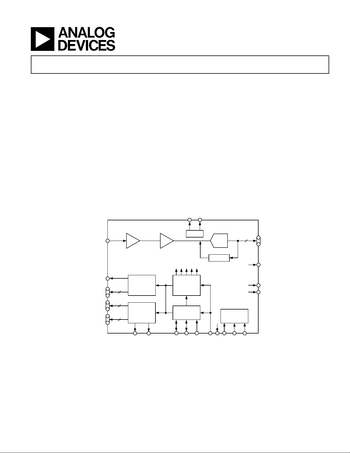
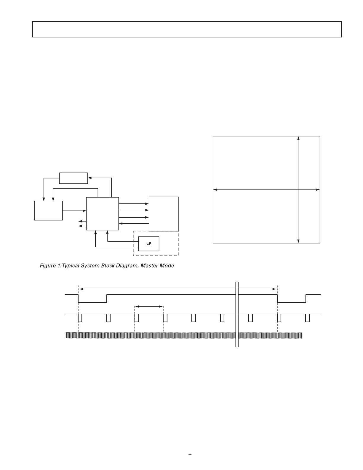
FUNCTIONAL BLOCK DIAGRAM
GENERAL DESCRIPTION
The AD9995 is a highly integrated CCD signal processor for
digital still camera and camcorder applications. It includes a
complete analog front end with A/D conversion, combined with a
full-function programmable timing generator. The timing generator is capable of supporting both 4- and 6-phase vertical clocking.
A Precision Timing core allows adjustment of high speed clocks
with less than 600 ps resolution at 36 MHz operation.
The AD9995 is specied at pixel rates of up to 36 MHz. The
analog front end includes black level clamping, CDS, VGA,
and a 12-bit A/D converter. The timing generator provides all
the necessary CCD clocks: RG, H-clocks, V-clocks, sensor gate
pulses, substrate clock, and substrate bias control. Operation is
programmed using a 3-wire serial interface.
Packaged in a space-saving 56-lead LFCSP, the AD9995 is specied over an operating temperature range of –20°C to +85°C.
REV. 0
Information furnished by Analog Devices is believed to be accurate and
reliable. However, no responsibility is assumed by Analog Devices for its
use, nor for any infringements of patents or other rights of third parties
that may result from its use. No license is granted by implication or otherwise under any patent or patent rights of Analog Devices. Trademarks
and registered trademarks are the property of their respective owners.
One Technology Way, P.O. Box 9106, Norwood, MA 02062-9106, U.S.A.
Tel: 781/329-4700 www.analog.com
Fax: 781/326-8703 © 2003 Analog Devices, Inc. All rights reserved.

AD9995
TABLE OF CONTENTS
SPECIFICATIONS . . . . . . . . . . . . . . . . . . . . . . . . . . . . . . . 3
Digital Specications . . . . . . . . . . . . . . . . . . . . . . . . . . . . . 3
AD9995 Analog Specications . . . . . . . . . . . . . . . . . . . . . . 4
Timing Specications . . . . . . . . . . . . . . . . . . . . . . . . . . . . . 5
ABSOLUTE MAXIMUM RATINGS . . . . . . . . . . . . . . . . . . 5
PACKAGE THERMAL CHARACTERISTICS. . . . . . . . . . . 5
ORDERING GUIDE. . . . . . . . . . . . . . . . . . . . . . . . . . . . . . . 5
PIN CONFIGURATION . . . . . . . . . . . . . . . . . . . . . . . . . . . 6
PIN FUNCTION DESCRIPTIONS . . . . . . . . . . . . . . . . . . . 6
TERMINOLOGY . . . . . . . . . . . . . . . . . . . . . . . . . . . . . . . . . 7
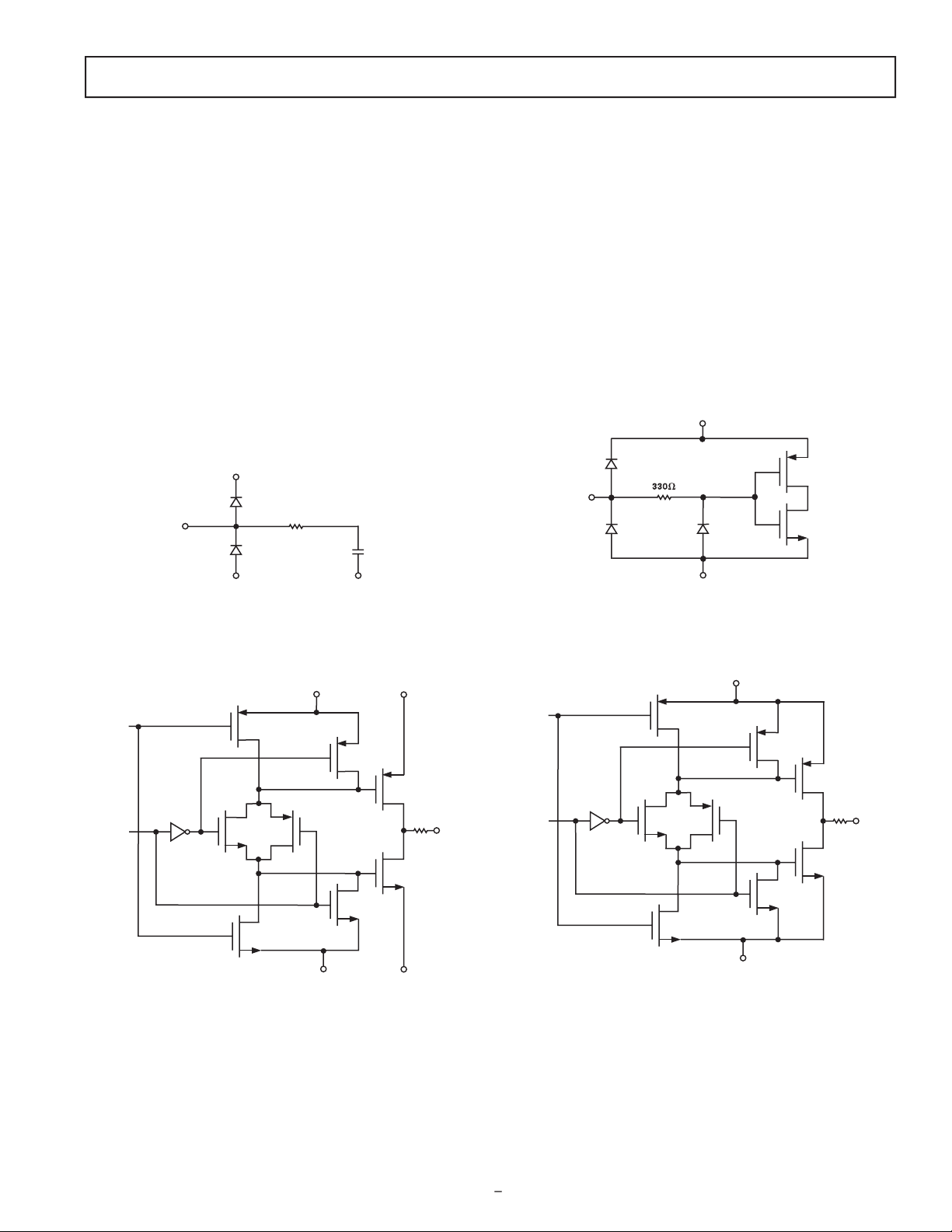
EQUIVALENT CIRCUITS . . . . . . . . . . . . . . . . . . . . . . . . . . 7
TYPICAL PERFORMANCE CHARACTERISTICS . . . . . . 8
SYSTEM OVERVIEW. . . . . . . . . . . . . . . . . . . . . . . . . . . . . . 9
PRECISION TIMING HIGH SPEED TIMING
GENERATION . . . . . . . . . . . . . . . . . . . . . . . . . . . . . . . . . . 10
Timing Resolution. . . . . . . . . . . . . . . . . . . . . . . . . . . . . . . 10
High Speed Clock Programmability . . . . . . . . . . . . . . . . . 10
H-Driver and RG Outputs . . . . . . . . . . . . . . . . . . . . . . . . 11
Digital Data Outputs . . . . . . . . . . . . . . . . . . . . . . . . . . . . 11
HORIZONTAL CLAMPING AND BLANKING . . . . . . . . 13
Individual CLPOB and PBLK Patterns. . . . . . . . . . . . . . . 13
Individual HBLK Patterns . . . . . . . . . . . . . . . . . . . . . . . . 13
Generating Special HBLK Patterns. . . . . . . . . . . . . . . . . . 14
Generating HBLK Line Alternation . . . . . . . . . . . . . . . . . 14
HORIZONTAL TIMING SEQUENCE EXAMPLE . . . . . . 15
VERTICAL TIMING GENERATION . . . . . . . . . . . . . . . . 16
Vertical Pattern Groups (VPAT) . . . . . . . . . . . . . . . . . . . . 17
Vertical Sequences (VSEQ) . . . . . . . . . . . . . . . . . . . . . . . . 18
Complete Field: Combining V-Sequences . . . . . . . . . . . . . 19
Generating Line Alternation for V-Sequence and HBLK . . 20
Second V-Pattern Group during VSG Active Line . . . . . . . 20
Sweep Mode Operation. . . . . . . . . . . . . . . . . . . . . . . . . . . 21
Multiplier Mode . . . . . . . . . . . . . . . . . . . . . . . . . . . . . . . . 21
Vertical Sensor Gate (Shift Gate) Patterns . . . . . . . . . . . . . 22
MODE Register . . . . . . . . . . . . . . . . . . . . . . . . . . . . . . . . 23
VERTICAL TIMING EXAMPLE . . . . . . . . . . . . . . . . . . . . 24
Important Note about Signal Polarities . . . . . . . . . . . . . . . 24
SHUTTER TIMING CONTROL . . . . . . . . . . . . . . . . . . . . 26
Normal Shutter Operation . . . . . . . . . . . . . . . . . . . . . . . . 26
High Precision Shutter Operation . . . . . . . . . . . . . . . . . . . 26
Low Speed Shutter Operation . . . . . . . . . . . . . . . . . . . . . . 26
SUBCK Suppression . . . . . . . . . . . . . . . . . . . . . . . . . . . . 27
Readout after Exposure. . . . . . . . . . . . . . . . . . . . . . . . . . . 27
Using the TRIGGER Register. . . . . . . . . . . . . . . . . . . . . . 27
VSUB Control . . . . . . . . . . . . . . . . . . . . . . . . . . . . . . . . . 28
MSHUT and STROBE Control . . . . . . . . . . . . . . . . . . . . 28
TRIGGER Register Limitations . . . . . . . . . . . . . . . . . . . . 29
EXPOSURE AND READOUT EXAMPLE . . . . . . . . . . . . 30
AFE DESCRIPTION AND OPERATION . . . . . . . . . . . . . 31
DC Restore . . . . . . . . . . . . . . . . . . . . . . . . . . . . . . . . . . . 31
Correlated Double Sampler . . . . . . . . . . . . . . . . . . . . . . . 31
Variable Gain Amplier . . . . . . . . . . . . . . . . . . . . . . . . . . 31
A/D Converter . . . . . . . . . . . . . . . . . . . . . . . . . . . . . . . . . 32
Optical Black Clamp. . . . . . . . . . . . . . . . . . . . . . . . . . . . . 32
Digital Data Outputs . . . . . . . . . . . . . . . . . . . . . . . . . . . . 32
POWER-UP AND SYNCHRONIZATION . . . . . . . . . . . . . 33
Recommended Power-Up Sequence for Master Mode. . . . 33
Generating Software SYNC without
External SYNC Signal . . . . . . . . . . . . . . . . . . . . . . . . . 33
SYNC during Master Mode Operation . . . . . . . . . . . . . . . 34
Power-Up and Synchronization in Slave Mode . . . . . . . . . 34
STANDBY MODE OPERATION. . . . . . . . . . . . . . . . . . . . 34
CIRCUIT LAYOUT INFORMATION . . . . . . . . . . . . . . . . 36
SERIAL INTERFACE TIMING . . . . . . . . . . . . . . . . . . . . . 37
Register Address Banks 1 and 2. . . . . . . . . . . . . . . . . . . . . 38
Updating of New Register Values. . . . . . . . . . . . . . . . . . . . 39
COMPLETE LISTING OF REGISTER BANK 1 . . . . . . . 40
COMPLETE LISTING OF REGISTER BANK 2 . . . . . . . 43
OUTLINE DIMENSIONS . . . . . . . . . . . . . . . . . . . . . . . . . 59
–2– –3–
REV. 0 REV. 0

–3
AD9995–SPECIFICATIONS
Parameter
Typ
Max
Unit
TEMPERATURE RANGE
Operating
–20
+85
°C
Storage
–65
+150
°C
POWER SUPPLY VOLTAGE
AVDD (AFE Analog Supply)
2.7
3.0
3.6
V
TCVDD (Timing Core Analog Supply)
2.7
3.0
3.6
V
RGVDD (RG Driver)
2.7
3.0
3.6
V
HVDD (H1–H4 Drivers)
2.7
3.0
3.6
V
DRVDD (Data Output Drivers)
2.7
3.0
3.6
V
DVDD (Digital)
2.7
3.0
3.6
V
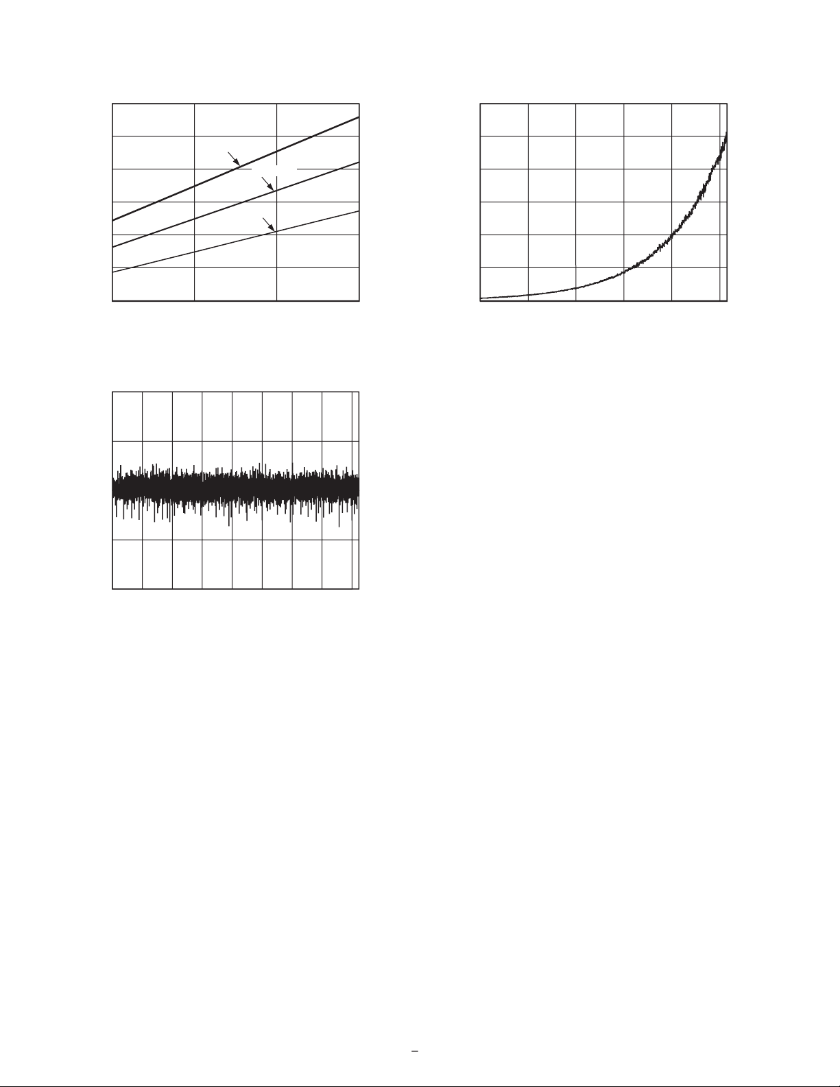
POWER DISSIPATION (See TPC 1 for Power Curves)
36 MHz, Typ Supply Levels, 100 pF H1–H4 Loading
360
mW
Power from HVDD Only
Number
Frequency
Frequency
V
V
V
V
V
V
V
V
V
VDD – 0.5
V
V
V
V p-p
VARIABLE GAIN AMPLIFIER (VGA)
–1.0
V
VOLTAGE REFERENCE
V
V
5.0
6.0
Code) + 6 dB
40.5
42.5
AC grounded input, 6 dB gain applied.
= 36 MHz, Typical
Speci cations, T
to T
–5
= 20 pF, AVDD = DVDD = DRVDD = 3.0 V, f
= 36 MHz, unless otherwise noted.)
(Figures 9 and 14)
(Figure 7)
AVSS
–0.3
V
–0.3
V
–0.3
V
–0.3
V
–0.3
V
–0.3
V
–0.3 V
–0.3 V
–0.3
V
–0.3 V
–0.3 V
AVSS
–0.3
V
Junction Temperature
JA
= 25°C/W
JA
–20°C to +85°C
–20°C to +85°C
–6
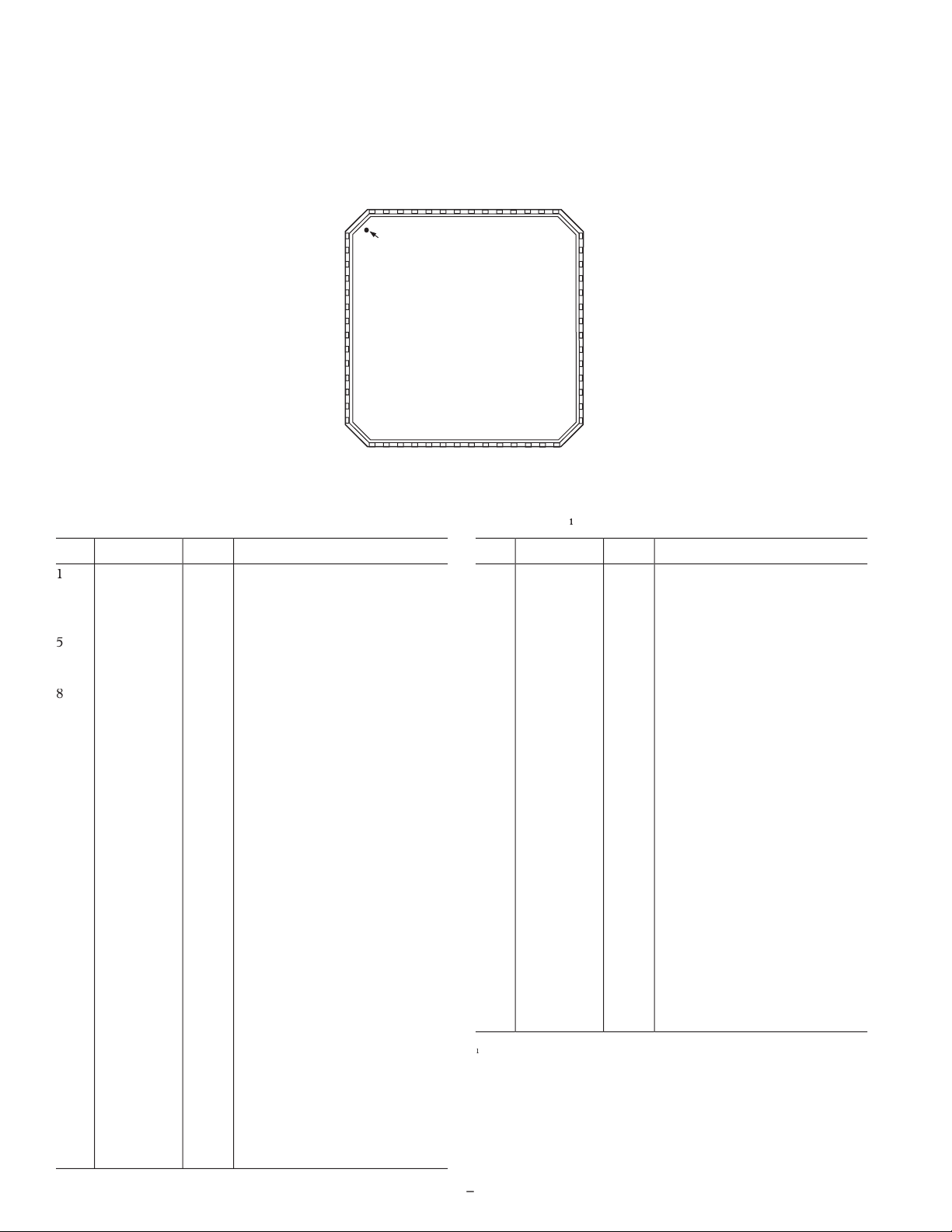
TOP VIEW
AD9995
PIN 1
IDENTIFIE
R
42 SDI
41 SL
40 REFB
39 REFT
38 AVSS
37 CCDIN
36 AVDD
35 CLI
34 CLO
33 TCVDD
D5 1
D6 2
D7 3
D8 4
D9 5
D10 6
(MSB) D11 7
DRVDD 8
DRVSS 9
VSUB 10
56 D4
55 D3
54 D2
53 D1
52 D0 (LSB)
51 DCLK
50 HD
49 DVDD
48 DVSS
47 VD
V4 15
V5 16
V6 17
VSG1 18
VSG2 19
VSG3 20
VSG4 21
VSG5 22
H1 23
H2 24
SUBCK 11
V1 12
V2 13
V3 14
HVSS 25
HVDD 26
H3 27
H4 28
32 TCVSS
31 RGVDD
30 RG
29 RGVSS
46 SYNC_CLP
45 STROBE
44 MSHUT
43 SCK
VSUB
V1
V2
V3
V4
V5
V6
VSG1
VSG2
VSG3
VSG4
VSG5
Analog Ground for Timing Core
Analog Supply for Timing Core
AVDD
Analog Supply for AFE
AI
AVSS
Analog Ground for AFE
AO
Voltage Reference Top Bypass
AO
Voltage Reference Bottom Bypass
VD
Vertical Sync Pulse
AI = Analog Input, AO = Analog Output, DI = Digital Input,
codes), where n is the bit resolution of the ADC. For the
R
AVDD
AVSS AVSS
DVDD
DVSS
DRVSS
DRVDD
THREE-
STATE
DATA
DOUT
DVDD
DVSS
HVDD OR
RGVDD
HVSS OR
RGVSS
OUTPUT
RG, H1–H4
ENABLE
–8
SAMPLE RATE (MHz)
450
350
150
36
18
POWER DISSIPATION (mW)
250
300
400
24
VDD = 3.3V
VDD = 3.0V
VDD = 2.7V
200
30
0
1000
500
1500 2000 2500 3000 3500 4000
0
–1.0
1.0
–0.5
0.5
CODES
DNL (LSB)
VGA GAIN CODE (LSB)
48
0
0
1000
400
200
600 800
OUTPUT NOISE (LSB)
16
32
8
24
40
–9
CCDIN
MSHUT
STROBE
H1–H4, RG, VSUB
V1–V6,
VSG1–VSG5, SUBCK
CCD
V-DRIVER
AD9995
AFETG
DIGITAL
IMAGE
PROCESSING
ASIC
DOUT
DCLK
HD, VD
CLI
SERIAL
INTERFACE
SYNC
vertical clocking is controlled by these counters to specify line
12-BIT HORIZONTAL = 4096 PIXELS MAX
12-BIT VERTICAL = 4096 LINES MAX
MAXIMUM
FIELD
DIMENSIONS
VD
HD
MAX VD LENGTH IS 4095 LINES
CLI
MAX HD LENGTH IS 4095 PIXELS

–10
master clock input (CLI)
system clock is not available, it
reference clock by programming the
valid edge locations available. Therefore, the register values are
NOTES
PIXEL CLOCK PERIOD IS DIVIDED INTO 48 POSITIONS, PROVIDING FINE EDGE RESOLUTION FOR HIGH SPEED CLOCKS.
THERE IS A FIXED DELAY FROM THE CLI INPUT TO THE INTERNAL PIXEL PERIOD POSITIONS
(t
CLIDLY
= 6ns TYP).
P[0] P[48] = P[0]P[12] P[24] P[36]
1 PIXEL
PERIOD
CLI
t
CLIDLY
POSITION
H1
H2
CCD
SIGNAL
RG
PROGRAMMABLE CLOCK POSITIONS:
1. RG RISING EDGE
2. RG FALLING EDGE
3. SHP SAMPLE LOCATION
4. SHD SAMPLE LOCATION
5. H1 RISING EDGE POSITION
7. H3 RISING EDGE POSITION
H3
H4
3
4
1 2
5 6
7 8
6. H1 FALLING EDGE POSITION (H2 IS INVERSE OF H1)
8. H3 FALLING EDGE POSITION (H4 IS INVERSE OF H3)
AD9995
H1/H3
H2/H4
RG
USING THE SAME TOGGLE POSITIONS FOR H1 AND H3 GENERATES STANDARD 2-PHASE H-CLOCKING.
CCD
SIGNAL
mapped into four quadrants, with each quadrant containing 12
edge locations. Table II shows the correct register values for the
corresponding edge locations.
Figure 7 shows the default timing locations for all of the high
speed clock signals.
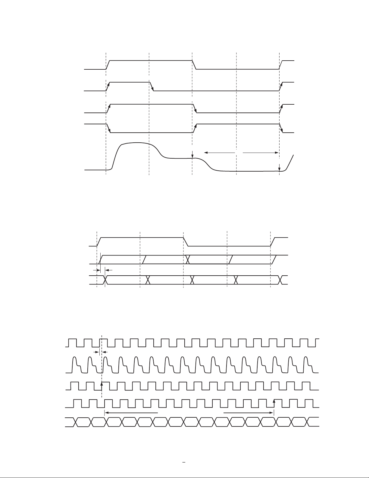
H-Driver and RG Outputs
In addition to the programmable timing positions, the AD9995
features on-chip output drivers for the RG and H1–H4 outputs.
These drivers are powerful enough to directly drive the CCD
inputs. The H-driver and RG current can be adjusted for optimum
rise/fall time into a particular load by using the DRVCONTROL
register (Addr. 0x35). The 3-bit drive setting for each output is
adjustable in 4.1 mA increments, with the minimum setting of 0
equal to OFF or three-state, and the maximum setting of 7 equal
to 30.1 mA.
As shown in Figures 5, 6, and 7, the H2 and H4 outputs are
inverses of H1 and H3, respectively. The H1/H2 crossover voltage is approximately 50% of the output swing. The crossover
Digital Data Outputs
The AD9995 data output and DCLK phases are programmable
using the DOUTPHASE register (Addr. 0x37, Bits [5:0]). Any
edge from 0 to 47 may be programmed, as shown in Figure 8a.
Normally, the DOUT and DCLK signals will track in phase
based on the DOUTPHASE register contents. The DCLK
output phase can also be held xed with respect to the data outputs by changing the DCLKMODE register high (Addr. 0x37,
Bit 6). In this mode, the DCLK output will remain at a xed
phase equal to CLO (the inverse of CLI) while the data output
phase is still programmable.
There is a xed output delay from the DCLK rising edge to the
DOUT transition, called tOD. This delay can be programmed to
four values between 0 ns and 12 ns by using the DOUTDELAY
register (Addr. 0x037, Bits [8:7]). The default value is 8 ns.
The pipeline delay through the AD9995 is shown in Figure 8b.
After the CCD input is sampled by SHD, there is an 11-cycle
delay until the data is available.
voltage is not programmable.
Table I. Timing Core Register Parameters for H1, H3, RG, SHP/SHD
Parameter Length Range Description
Polarity 1b High/Low Polarity Control for H1, H3, and RG (0 = No Inversion, 1 = Inversion)
Positive Edge 6b 0–47 Edge Location Positive Edge Location for H1, H3, and RG
Negative Edge 6b 0–47 Edge Location Negative Edge Location for H1, H3, and RG
Sampling Location 6b 0–47 Edge Location Sampling Location for Internal SHP and SHD Signals
Drive Strength 3b 0–47 Current Steps Drive Current for H1–H4 and RG Outputs (4.1 mA per Step)
Figure 6. 2-Phase H-Clock Operation
Table II. Precision Timing Edge Locations
Quadrant Edge Location (Dec) Register Value (Dec) Register Value (Bin)
I 0 to 11 0 to 11 000000 to 001011
II 12 to 23 16 to 27 010000 to 011011
III 24 to 35 32 to 43 100000 to 101011
IV 36 to 47 48 to 59 110000 to 111011
REV. 0
–11–
P[0]
PIXEL
PERIOD
RG
H1/H3
RGf[12]
P[48] = P[0]
Hf[24]
CCD
SIGNAL
P[24]P[12] P[36]
Hr[0]
RGr[0]
SHD[0]
NOTES
ALL SIGNAL EDGES ARE FULLY PROGRAMMABLE TO ANY OF THE 48 POSITIONS WITHIN ONE PIXEL PERIOD.
DEFAULT POSITIONS FOR EACH SIGNAL ARE SHOWN.
POSITION
t
S1
H2/H4
SHP[24]
NOTES
DATA OUTPUT (DOUT) AND DCLK PHASE ARE ADJUSTABLE WITH RESPECT TO THE PIXEL PERIOD.
WITHIN ONE CLOCK PERIOD, THE DATA TRANSITION CAN BE PROGRAMMED TO 48 DIFFERENT LOCATIONS
.
OUTPUT DELAY (tOD) FROM DCLK RISING EDGE TO DOUT RISING EDGE IS PROGRAMMABLE.
P[0] P[48] = P[0]
PIXEL
PERIOD
P[12] P[24] P[36]
DOUT
DCLK
t
OD
NOTES
DEFAULT TIMING VALUES ARE SHOWN: SHDLOC = 0, DOUT PHASE = 0, DCLKMODE = 0.
HIGHER VALUES OF SHD AND/OR DOUTPHASE WILL SHIFT DOUT TRANSITION TO THE RIGHT, WITH RESPECT TO CLI LOCATION.
DCLK
DOUT
CCDIN
CLI
SHD
(INTERNAL)
N N+1
N+2
N+12N+11N+10N+9N+8N+7N+6N+5N+4
N+3
N+13
N–13
N–3N–4N–5N–6N–7N–8N–9N–10N–11
N–12
N–2
N–1
N+1
N
SAMPLE PIXEL N
PIPELINE LATENCY=11 CYCLES
t
CLIDLY
N–1
N+2
AD9995
(3)(2)
(1)
HD
CLPOB
PBLK
. . .
NOTES
PROGRAMMABLE SETTINGS:
1. START POLARITY (CLAMP AND BLANK REGION ARE ACTIVE LOW)
2. FIRST TOGGLE POSITION
3. SECOND TOGGLE POSITION
. . .
ACTIVE
ACTIV
E
HORIZONTAL CLAMPING AND BLANKING
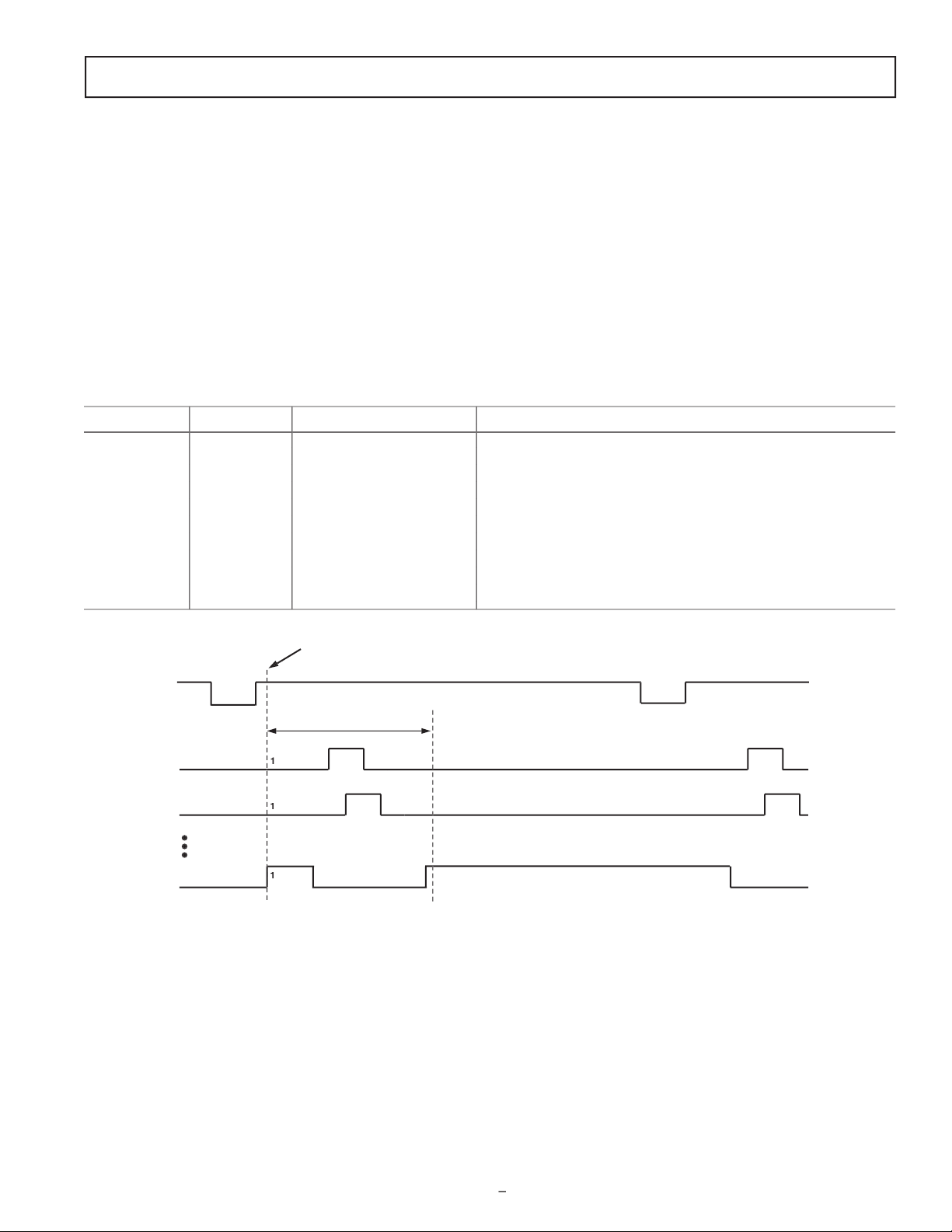
The AD9995’s horizontal clamping and blanking pulses are fully
programmable to suit a variety of applications. Individual control
is provided for CLPOB, PBLK, and HBLK during the different
regions of each eld. This allows the dark pixel clamping and
blanking patterns to be changed at each stage of the readout in
order to accommodate different image transfer timing and high
speed line shifts.
Individual CLPOB and PBLK Patterns
The AFE horizontal timing consists of CLPOB and PBLK, as
shown in Figure 9. These two signals are independently programmed using the registers in Table III. SPOL is the start
polarity for the signal, and TOG1 and TOG2 are the rst and
second toggle positions of the pulse. Both signals are active low
and should be programmed accordingly.
A separate pattern for CLPOB and PBLK may be programmed
for every 10 V-sequences. As described in the Vertical Timing
Generation section, up to 10 separate V-sequences can be created,
each containing a unique pulse pattern for CLPOB and PBLK.
Figure 9 shows how the sequence change positions divide the
readout eld into different regions. A different V-sequence can be
assigned to each region, allowing the CLPOB and PBLK signals
to be changed accordingly with each change in the vertical timing.
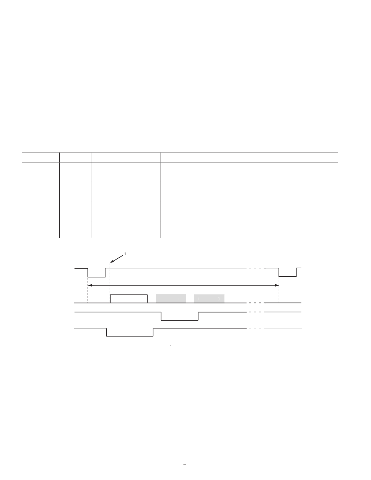
Individual HBLK Patterns
The HBLK programmable timing shown in Figure 10 is similar to CLPOB and PBLK. However, there is no start polarity
control. Only the toggle positions are used to designate the start
and stop positions of the blanking period. Additionally, there is a
polarity control HBLKMASK that designates the polarity of the
horizontal clock signals H1–H4 during the blanking period. Setting HBLKMASK high will set H1 = H3 = low and H2 = H4 =
high during the blanking, as shown in Figure 11. As with the
CLPOB and PBLK signals, HBLK registers are available in each
V-sequence, allowing different blanking signals to be used with
different vertical timing sequences.
Figure 9. Clamp and Pre-Blank Pulse Placement
Table III. CLPOB and PBLK Pattern Registers
Register Length Range Description
SPOL 1b High/Low Starting Polarity of CLPOB/PBLK for V-Sequence 0–9
TOG1 12b 0–4095 Pixel Location First Toggle Position within Line for V-Sequence 0–9
TOG2 12b 0–4095 Pixel Location Second Toggle Position within Line for V-Sequence 0–9
Table IV. HBLK Pattern Registers
Register Length Range Description
HBLKMASK 1b High/Low Masking Polarity for H1/H3 (0 = H1/H3 Low, 1 = H1/H3 High)
HBLKALT 2b 0–3 Alternation Mode Enables Odd/Even Alternation of HBLK Toggle Positions 0 =
Disable Alternation. 1 = TOG1–TOG2 Odd, TOG3–TOG6 Even.
2 = 3 = TOG1–TOG2 Even, TOG3–TOG6 Odd
HBLKTOG1 12b 0–4095 Pixel Location First Toggle Position within Line for Each V-Sequence 0–9
HBLKTOG2 12b 0–4095 Pixel Location Second Toggle Position within Line for Each V-Sequence 0–9
HBLKTOG3 12b 0–4095 Pixel Location Third Toggle Position within Line for Each V-Sequence 0–9
HBLKTOG4 12b 0–4095 Pixel Location Fourth Toggle Position within Line for Each V-Sequence 0–9
HBLKTOG5 12b 0–4095 Pixel Location Fifth Toggle Position within Line for Each V-Sequence 0–9
HBLKTOG6 12b 0–4095 Pixel Location Sixth Toggle Position within Line for Each V-Sequence 0–9
REV. 0
–13–
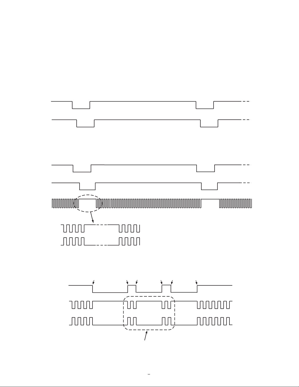
HD
HBLK
PROGRAMMABLE SETTINGS:
1. FIRST TOGGLE POSITION = START OF BLANKING
2. SECOND TOGGLE POSITION = END OF BLANKING
BLANK BLANK
1 2
HD
HBLK
THE POLARITY OF H1 DURING BLANKING IS PROGRAMMABLE (H2 IS OPPOSITE POLARITY OF H1).
H1/H3
H1/H3
H2/H4
HBLK
SPECIAL H-BLANK PATTERN IS CREATED USING MULTIPLE HBLK TOGGLE POSITIONS
.
H1/H3
H2/H4
TOG1
TOG2 TOG3
TOG4 TOG5 TOG6
–15
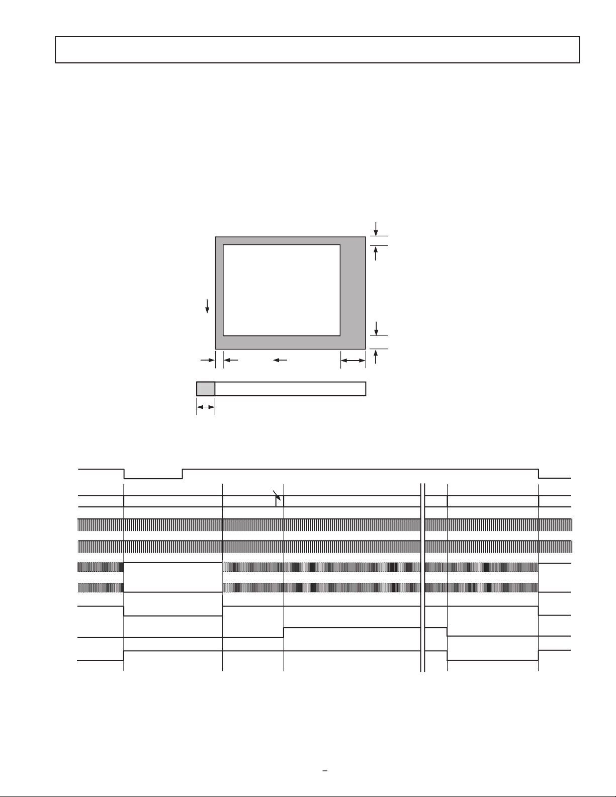
V
H
HORIZONTAL CCD REGISTER
EFFECTIVE IMAGE AREA
48 OB PIXELS
4 OB PIXELS
10 VERTICAL OB LINES
2 VERTICAL OB LINES
VERTICAL SHIFT
VERT SHIF
T
CCDIN
SHP
SHD
H1/H3
H2/H
HBLK
PBLK
CLPOB
OPTICAL BLACK
DUMMY
EFFECTIVE PIXELS
OB
OPTICAL BLACK
HD
–16
vertical CCD timing, and can support multiple CCDs and dif-
V1–V6 are used to shift each line of pixels into the horizontal
REGION 0: USE V-SEQUENCE 3
REGION 1: USE V-SEQUENCE 2
REGION 2: USE V-SEQUENCE 1
REGION 0: USE V-SEQUENCE 3
REGION 1: USE V-SEQUENCE 2
REGION 2: USE V-SEQUENCE 1
REGION 0: USE V-SEQUENCE 2
REGION 1: USE V-SEQUENCE 0
REGION 3: USE V-SEQUENCE 0
REGION 4: USE V-SEQUENCE 2
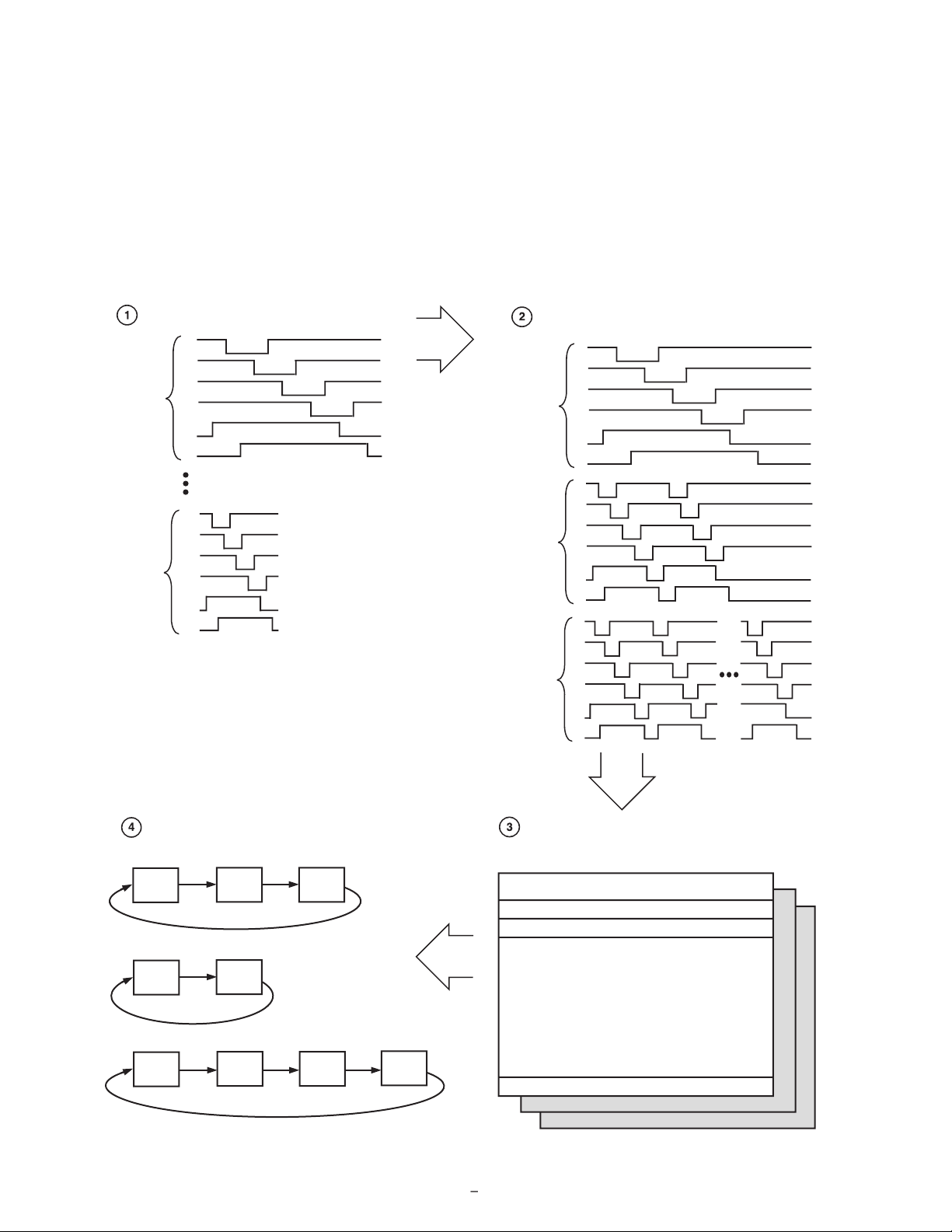
CREATE THE VERTICAL PATTERN GROUPS
(MAXIMUM OF 10 GROUPS).
BUILD THE V-SEQUENCES BY ADDING LINE START
POSITION, # OF REPEATS, AND HBLK/CLPOB PULSES
(MAXIMUM OF 10 V-SEQUENCES).
V-SEQUENCE 0
(VPAT0, 1 REP)
BUILD EACH FIELD BY DIVIDING INTO DIFFERENT REGIONS,
AND ASSIGNING A DIFFERENT V-SEQUENCE TO EACH
(MAXIMUM OF 7 REGIONS IN EACH FIELD
)
(MAXIMUM OF 6 FIELDS).
V1
V2
V5
V6
V1
V2
V3
V4
FIELD 0
FIELD 1
FIELD 2
REGION 2: USE V-SEQUENCE 3
USE THE MODE REGISTER TO CONTROL WHICH FIELDS
ARE USED, AND IN WHAT ORDER
(MAXIMUM OF 7 FIELDS MAY BE COMBINED IN ANY ORDER).
FIELD 0
FIELD 1 FIELD 2
FIELD 3
FIELD 4
FIELD 5
FIELD 1 FIELD 4
FIELD 2
V4
V3
V5
V6
V-SEQUENCE 1
(VPAT9, 2 REP)
V-SEQUENCE
2
(VPAT9, N REP)
VPAT 0
V1
V2
V5
V6
V4
V3
V1
V2
V5
V6
V4
V3
V1
V2
V5
V6
V4
V3
VPAT 9
VPOL
VTOG1
VTOG2
VTOG3
VTOG4
VPATLEN
VTOG2, VTOG3) are the pixel locations within the line where
vided, allowing the vertical outputs to be interrupted twice in
Vertical Sequence section.
–18
V-pattern groups and adding repeats, start position, and hori-
VPATSEL
VMASK
VPATREPO
VPATREPE
VPATSTART
 Loading...