ANALOG DEVICES AD9956 Service Manual
2.7 GHz DDS-Based
Agile
RFTM Synthesizer
FEATURES
400 MSPS internal DDS clock speed
48-bit frequency tuning word
14-bit programmable phase offset
Integrated 14-bit DAC
Excellent dynamic performance
Phase noise ≤ 135 dBc/Hz @ 1 KHz offset
−80 dB SFDR @ 160 MHz (±100 KHz offset I
25 Mb/s write-speed serial I/O control
200 MHz phase frequency detector inputs
655 MHz programmable input dividers for the phase
frequency detector (÷M, ÷N) {M, N = 1..16} (bypassable)
Programmable RF divider (÷R) {R = 1, 2, 4, 8} (bypassable)
8 phase/frequency profiles
1.8 V supply for device operation
DELTA
FREQUENCY
PLL_LOCK/SYNC_IN
I/O_UPDATE
SYNC_OUT
REFCLK
REFCLK
TUNING WORD
SYNC_CLK
CML CLOCK DRIVER
24
FREQUENCY
ACCUMULATOR
DELTA
FREQUENCY
RAMP RATE
RF-DIVIDER
÷R
)
OUT
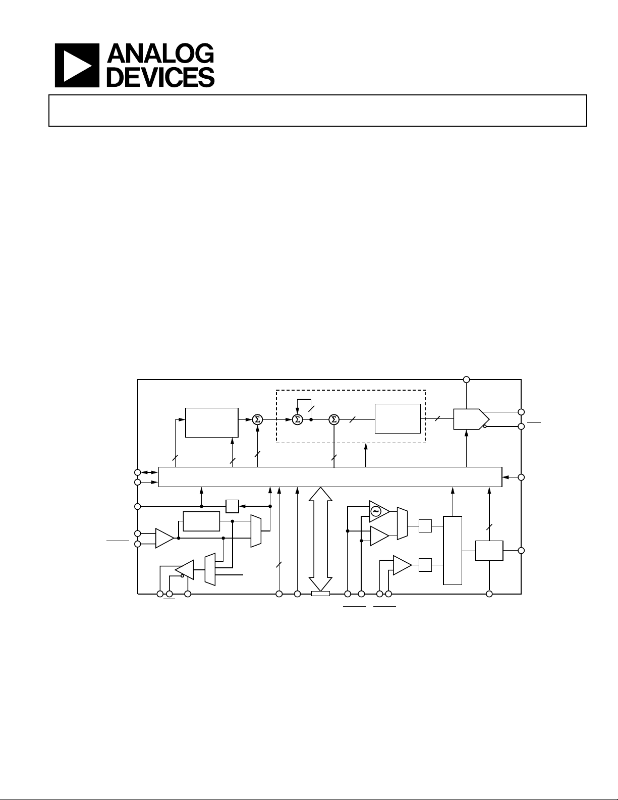
FUNCTIONAL BLOCK DIAGRAM
FTW
48
16
TIMING AND CONTRO LLOGIC
SYSCLK
÷4
3
FROM PLLOSC
48
PHASE
ACCUMULATOR
PHASE
OFFSET
WORD
AD9956
3.3 V supply for I/O and charge pump
Software controlled power-down
48-lead LFCSP package
Automatic linear frequency sweeping capability (in DDS)
Programmable charge pump current (up to 4 mA)
Phase modulation capability
Multichip synchronization
Dual-mode PLL lock detect
655 MHz CML-mode PECL-compliant driver
APPLICATIONS
Agile LO frequency synthesis
FM chirp source for radar and scanning systems
Automotive radars
Test and measurement equipment
Acousto-optic device drivers
DAC_RSET
PHASE
OFFSET
DDS CORE
19 14
14
PHASE TO
AMPLITUDE
CONVERSION
SYSCLK
OSCILLATOR
BUFFER
LOCK
DETECT
÷M
÷N
DAC
SYSCLK
CHARGE
PUMP
SCALER
3
ΦBUFFER
CHARGE
PUMP
IOUT
IOUT
I/O_RESET
CP_OUT
DRV DRV DRV_RSET
PS<2:0>
RESET I/O PORT
Rev. A
Information furnished by Analog Devices is believed to be accurate and reliable.
However, no responsibility is assumed by Analog Devices for its use, nor for any
infringements of patents or other rights of third parties that may result from its use.
Specifications subject to change without notice. No license is granted by implication
or otherwise under any patent or patent rights of Analog Devices. Trademarks and
registered trademarks are the property of their respective owners.
Figure 1.
PLLREF/
PLLREF
One Technology Way, P.O. Box 9106, Norwood, MA 02062-9106, U.S.A.
Tel: 781.329.4700
Fax: 781.326.8703 © 2004 Analog Devices, Inc. All rights reserved.
PLLOSC/
PLLOSC
www.analog.com
CP_RSET
04806-0-001

AD9956
TABLE OF CONTENTS
Product Overview............................................................................. 3
CML Driver................................................................................. 19
Specifications..................................................................................... 4
Loop Measurement Conditions.................................................. 9
Absolute Maximum Ratings.......................................................... 10
ESD Caution................................................................................ 10
Pin Configuration and Function Descriptions........................... 11
Typical Performance Characteristics........................................... 13
Typical Application Circuits .......................................................... 16
Application Circuit Explanations ............................................. 17
General Description....................................................................... 18
DDS Core..................................................................................... 18
PLL Circuitry .............................................................................. 18
REVISION HISTORY
9/04—Data Sheet Changed from Rev. 0 to Rev. A
Changes to the Pin Configuration................................................ 11
Changes to the Pin Function Descriptions ................................. 12
Changes to Table 5.......................................................................... 24
Changes to CFR2<15:12> PLLREF Divider
Control Bits (÷N)............................................................................ 31
Changes to CFR2<11:8> PLLREF Divider
Control Bits (÷M)........................................................................... 31
Changes to Ordering Guide.......................................................... 32
Modes of Operation ....................................................................... 20
DDS Modes of Operation ......................................................... 20
Synchronization Modes for Multiple Devices .............................. 20
Serial Port Operation..................................................................... 22
Instruction Byte .......................................................................... 23
Serial Interface Port Pin Description....................................... 23
MSB/LSB Transfers .................................................................... 23
Register Map and Description ...................................................... 24
Control Function Register Descriptions ................................. 27
Outline Dimensions....................................................................... 32
Ordering Guide .......................................................................... 32
7/04—Revision: Initial Version
Rev. A | Page 2 of 32

AD9956
PRODUCT OVERVIEW
The AD9956 is Analog Devices’ newest AgileRF synthesizer.
The device is comprised of DDS and PLL circuitry. The DDS
features a 14-bit DAC operating at up to 400 MSPS and a 48-bit
frequency tuning word (FTW). The PLL circuitry includes a
phase frequency detector with scaleable 200 MHz inputs
(divider inputs operate up to 655 MHz) and digital control over
the charge pump current. The device also includes a 655 MHz
CML-mode PECL-compliant driver with programmable slew
rates. The AD9956 uses advanced DDS technology, an internal
high speed, high performance DAC, and an advanced phase
frequency detector/charge pump combination, which, when
used with an external VCO, enables the synthesis of digitally
programmable, frequency-agile analog output sinusoidal waveforms up to 2.7 GHz. The AD9956 is designed to provide fast
frequency hopping and fine tuning resolution (48-bit frequency
tuning word). Information is loaded into the AD9956 via a
serial I/O port that has a device write-speed of 25 Mb/s. The
AD9956 DDS block also supports a user-defined linear sweep
mode of operation.
The AD9956 is specified to operate over the extended
automotive range of −40°C to +125°C.
Rev. A | Page 3 of 32

AD9956
SPECIFICATIONS
AVDD = DVDD = 1.8 V ± 5%; DVDD_I/O = CP_VDD = 3.3 V ± 5% (@ TA = 25°C) DAC_R
DRV_R
= 4.02 kΩ, unless otherwise noted.
SET
Table 1.
Parameter Min Typ Max Unit Test Conditions/Comments
RF DIVIDER (REFCLK ) INPUT SECTION (÷R)
RF Divider Input Range 1 2700 MHz
Input Capacitance (DC) 3 pF
Input Impedance (DC) 1500 Ω
Input Duty Cycle 42 50 58 %
Input Power/Sensitivity −10 +4 dBm Single-ended, into a 50 Ω load
Input Voltage Level 350 1000 mV p-p
PHASE FREQUENCY DETECTOR/CHARGE PUMP
PLLREF Input
Input Frequency
2
÷M Set to Divide by at Least 4 655 MHz
÷M Bypassed 200 MHz
Input Voltage Levels 200 450 600 mV p-p
Input Capacitance 10 pF
Input Resistance 1500 Ω
PLLOSC Input
Input Frequency
÷N Set to Divide by at Least 4 655 MHz
÷N Bypassed 200 MHz
Input Voltage Levels 200 450 600 mV p-p
Input Capacitance 10 pF
Input Resistance 1500 Ω
Charge Pump Source/Sink Maximum Current 4 mA
Charge Pump Source/Sink Accuracy −15 +5 %
Charge Pump Source/Sink Matching −5 +5 %
Charge Pump Output Compliance Range
3
0.5 CP_VDD − 0.5 V
PLL_LOCK Drive Strength 2 mA
PHASE FREQUENCY DETECTOR NOISE FLOOR
@ 50 kHz PFD Frequency 149 dBc/Hz
@ 2 MHz PFD Frequency 133 dBc/Hz
@ 100 MHz PFD Frequency 116 dBc/Hz
@ 200 MHz PFD Frequency 113 dBc/Hz
CML OUTPUT DRIVER (DRV)
Differential Output Voltage Swing
4
720 mV 50 Ω load to supply, both lines
Maximum Toggle Rate 655 MHz
Common-Mode Output Voltage 1.75 V
Output Duty Cycle 42 50 58 %
Output Current
Continuous
5
7.2 mA
Rising Edge Surge 20.9 mA
Falling Edge Surge 13.5 mA
Output Rise Time 250 ps 100 Ω terminated, 5 pF load
= 3.92 kΩ, CP_R
SET
DDS SYSCLK not to exceed
400 MSPS
= 3.09 kΩ,
SET
1
Rev. A | Page 4 of 32

AD9956
Parameter Min Typ Max Unit Test Conditions/Comments
LOGIC INPUTS (SDI/O, I/O_RESET, RESET,
I/O_UPDATE, PS0 to PS2, SYNC_IN)
VIH, Input High Voltage 2.0 V
VIL, Input Low Voltage 0.8 V
I
, I
Input Current ±1 ±5 µA
INH
INL
CIN, Maximum Input Capacitance 3 pF
LOGIC OUTPUTS (SDO, SYNC_OUT, PLL_LOCK)6
VOH, Output High Voltage 2.7 V
VOH, Output Low Voltage 0.4 V
I
OH
I
OL
POWER CONSUMPTION
Total Power Consumed, All Functions On 400 mW
IAVDD 85 mA
IDVDD 45 mA
IDVDD_I/O 20 mA
ICP_VDD 15 mA
Power-Down Mode 80 mW
WAKE-UP TIME (from Power-Down Mode)
Digital Power-Down (CFR1<7>) 12 ns
DAC Power-Down (CFR2<39>) 7 µs
RF Divider Power-Down (CFR2<23>) 400 ns
Clock Driver Power-Down (CFR2<20>) 6 µs
Charge Pump Full Power-Down (CFR2<4>) 10 µs
Charge Pump Quick Power-Down (CFR2<3>) 150 ns
DAC OUTPUT CHARACTERISTICS
Resolution 14 Bits
Full-Scale Output Current 10 15 mA
Gain Error −10 +10 % FS
Output Offset 0.6 µA
Output Capacitance 5 pF
Voltage Compliance Range AVDD − 0.50 AVDD + 0.50 V
Wideband SFDR (DC to Nyquist)
10 MHz Analog Out −64 dBc
40 MHz Analog Out −62 dBc
80 MHz Analog Out −60 dBc
120 MHz Analog Out −55 dBc
160 MHz Analog Out −55 dBc
Narrowband SFDR
10 MHz Analog Out (±1 MHz) −89 dBc
10 MHz Analog Out (±250 kHz) −91 dBc
10 MHz Analog Out (±50 kHz) −93 dBc
40 MHz Analog Out (±1 MHz) −87 dBc
40 MHz Analog Out (±250 kHz) −89 dBc
40 MHz Analog Out (±50 kHz) −91 dBc
80 MHz Analog Out (±1 MHz) −85 dBc
80 MHz Analog Out (±250 kHz) −87 dBc
80 MHz Analog Out (±50 kHz) −89 dBc
120 MHz Analog Out (±1 MHz) −83 dBc
120 MHz Analog Out (±250 kHz) −85 dBc
120 MHz Analog Out (±50 kHz) −87 dBc
100 µA
100 µA
Rev. A | Page 5 of 32
AD9956
Parameter Min Typ Max Unit Test Conditions/Comments
160 MHz Analog Out (±1 MHz) −81 dBc
160 MHz Analog Out (±250 kHz) −83 dBc
160 MHz Analog Out (±50 kHz) −85 dBc
DAC Residual Phase Noise
19.7 MHz F
OUT
@ 10 Hz Offset 125 dBc/Hz
@ 100 Hz Offset 135 dBc/Hz
@ 1 kHz Offset 143 dBc/Hz
@ 10 kHz Offset 152 dBc/Hz
@ 100 kHz Offset 158 dBc/Hz
>1 MHz Offset 163 dBc/Hz
51.84 MHz F
OUT
@ 10 Hz Offset 119 dBc/Hz
@ 100 Hz Offset 125 dBc/Hz
@ 1 kHz Offset 132 dBc/Hz
@ 10 kHz Offset 142 dBc/Hz
@ 100 kHz Offset 150 dBc/Hz
>1 MHz Offset 155 dBc/Hz
105.3 MHz Analog Out
@ 10 Hz Offset 105 dBc/Hz
@ 100 Hz Offset 115 dBc/Hz
@ 1 kHz Offset 122 dBc/Hz
@ 10 kHz Offset 131 dBc/Hz
@ 100 kHz Offset 139 dBc/Hz
>1 MHz Offset 142 dBc/Hz
155.52 MHz Analog Out
@ 10 Hz Offset 105 dBc/Hz
@ 100 Hz Offset 110 dBc/Hz
@ 1 kHz Offset 119 dBc/Hz
@ 10 kHz Offset 127 dBc/Hz
@ 100 kHz Offset 135 dBc/Hz
>1 MHz Offset 142 dBc/Hz
CRYSTAL OSCILLATOR (ON PLLREF INPUT)
Operating Range 20 25 30 MHz
Residual Phase Noise (@ 25 MHz)
@ 10 Hz Offset 95 dBc/Hz
@ 100 Hz Offset 120 dBc/Hz
@ 1 kHz Offset 137 dBc/Hz
@ 10 kHz Offset 156 dBc/Hz
@ 100 kHz Offset 164 dBc/Hz
>1 MHz Offset 170 dBc/Hz
DIGITAL TIMING SPECIFICATIONS
CS
to SCLK Setup Time TPRE
Period of SCLK (Write Speed) TSCLKW 40 ns
Period of SCLK (Read Speed) TSCLKR 400 ns
Serial Data Setup Time TDSU 6.5 ns
Serial Data Hold Time TDHLD 0 ns
TDV Data Valid Time TDV 40 ns
I/O Update to SYNC_CLK Setup Time TUD 7 ns
PS<2:0> to SYNC_CLK Setup Time TPS 7 ns
6 ns
Rev. A | Page 6 of 32

AD9956
Parameter Min Typ Max Unit Test Conditions/Comments
Latencies/Pipeline Delays
I/O Update to DAC Frequency Change 33 SYSCLK Cycles
I/O Update to DAC Phase Change 33 SYSCLK Cycles
PS<2:0> to DAC Frequency Change 29 SYSCLK Cycles
PS<2:0> to DAC Phase Change 29 SYSCLK Cycles
I/O Update to CP_OUT Scaler Change 4 SYSCLK Cycles
I/O Update to Frequency Accumulator
Step Size Change
I/O Update to Frequency Accumulator
Ramp Rate Change
RF DIVIDER/CML DRIVER EQUIVALENT
INTRINSIC TIME JITTER
FIN = 414.72 MHz, F
BW = 12 kHz −> 400 kHz 136 fS rms OC1, RF Divider R = 8
FIN = 1244.16 MHz, F
BW = 12 kHz −> 1.3 MHz 101 fS rms OC3, RF Divider R = 8
FIN = 2488.32 MHz, F
BW = 12 kHz −> 5 MHz 108 fS rms OC12, RF Divider R = 4
RF DIVIDER/CML DRIVER RESIDUAL PHASE NOISE
FIN = 157.6 MHz, F
@ 10 Hz −115 dBc/Hz
@ 100 Hz −126 dBc/Hz
@ 1 kHz −134 dBc/Hz
@ 10 kHz −143 dBc/Hz
@ 100 kHz −150 dBc/Hz
> 1 MHz −151 dBc/Hz
FIN = 1240 MHz, F
OUT
@ 10 Hz −111 dBc/Hz
@ 100 Hz −122 dBc/Hz
@ 1 kHz −129 dBc/Hz
@ 10 kHz −138 dBc/Hz
@ 100 kHz −146 dBc/Hz
@ 1 MHz −150 dBc/Hz
>3 MHz −153 dBc/Hz
FIN = 2488MHz, F
OUT
@ 10 Hz −97 dBc/Hz
@ 100 Hz −110 dBc/Hz
@ 1 kHz −120 dBc/Hz
@ 10 kHz −126 dBc/Hz
@ 100 kHz −136 dBc/Hz
@ 1 MHz −141 dBc/Hz
>3 MHz −144 dBc/Hz
TOTAL SYSTEM TIME JITTER FOR 622 MHz CLOCK
12 kHz to 5 MHz Bandwidth 0.7 ps rms
7
4 SYSCLK Cycles
4 SYSCLK Cycles
= 51.84 MHz
OUT
= 155.52 MHz
OUT
= 622.08 MHz
OUT
= 19.7 MHz RF Divider R = 8
OUT
= 155 MHz RF Divider R = 8
= 622 MHz RF Divider R = 4
See the Loop Measurement Conditions section
Rev. A | Page 7 of 32
AD9956
Parameter Min Typ Max Unit Test Conditions/Comments
TOTAL SYSTEM JITTER AND PHASE NOISE FOR
105.33 MHz ADC CLOCK GENERATION CIRCUIT
Converter Limiting Jitter 0.53 ps rms
Resultant SNR 67 dB
Phase Noise of Fundamental
@ 10 Hz Offset −75 dBc/Hz
@ 100 Hz Offset −87 dBc/Hz
@ 1 kHz Offset −93 dBc/Hz
@ 10 kHz Offset −105 dBc/Hz
@ 100 kHz Offset −145 dBc/Hz
@ ≥1 MHz Offset −152 dBc/Hz
See the Loop Measurement Conditions section
DRV
.
1
The input impedance of the REFCLK input is 1500 Ω. However, in order to provide matching on the clock line, an external 50 Ω load is used.
2
Driving the PLLREF input buffer, the crystal oscillator section of this input stage performs up to only 30 MHz.
3
The charge pump output compliance range is functionally 0.2 V to (CP_VDD − 0.2 V). The value listed here is the compliance range for 5% matching.
4
Measured as peak-to-peak from DRV to
5
For a 4.02 kΩ resistor from DRV_RSET to GND.
6
Assumes a 1 mA load.
7
I/O_UPDATE/PS<2:0> are detected by the AD9956 synchronous to the rising edge of SYNC_CLK. Each latency measurement is from the first SYNC_CLK rising edge
after the I/O_UPDATE/PS<2:0> state change.
Rev. A | Page 8 of 32
AD9956
LOOP MEASUREMENT CONDITIONS
622 MHz OC-12 Clock
VCO = Sirenza 190-640T
105 MHz Converter Clock
VCO = Sirenza 190-845T
Reference = Wenzel 500-10116 (30.3 MHz)
Loop Filter = 10 kHz BW, 60° Phase Margin
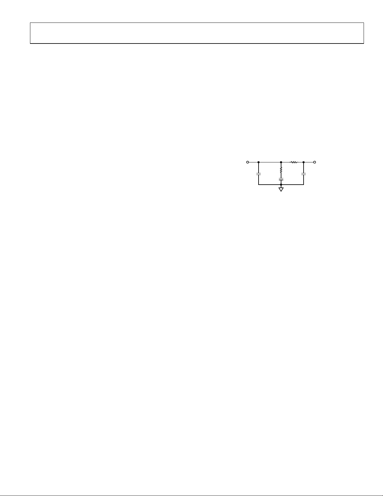
C1 = 170 nF, R1 = 14.4 Ω, C2 = 5.11 µF, R2 = 89.3 Ω,
C3 Omitted
CP_OUT = 4 mA (Scaler = ×8)
÷R = 2, ÷M = 1, ÷N = 1
Reference = Wenzel 500-10116 (30.3 MHz)
Loop Filter = 10 kHz BW, 45° Phase Margin
C1 = 117 nF, R1 = 28 Ω, C2 = 1.6 µF, R2 = 57.1 Ω, C3 = 53.4 nF
CP_OUT = 4 mA (Scaler = ×8)
÷R = 8, ÷M = 1, ÷N = 1
INPUT OUTPUT
C1
Figure 2. Generic Loop Filter
R2
R1
C2
C3
04806-0-033
Rev. A | Page 9 of 32
AD9956
ABSOLUTE MAXIMUM RATINGS
Table 2.
Parameter Rating
Analog Supply Voltage (AVDD) 2 V
Digital Supply Voltage (DVDD) 2 V
Digital I/O Supply Voltage
(DVDD_I/0)
Charge Pump Supply Voltage
(CPVDD)
Maximum Digital Input Voltage −0.5 V to DVDD_I/O + 0.5 V
Storage Temperature −65°C to +150°C
Operating Temperature Range −40°C to +125°C
Lead Temperature Range
(Soldering 10 sec)
Junction Temperature 150°C
Thermal Resistance (θJA) 26°C/W
Stresses above those listed under Absolute Maximum Ratings
may cause permanent damage to the device. This is a stress
rating only; functional operation of the device at these or any
other conditions above those indicated in the operational
section of this specification is not implied. Exposure to absolute
maximum rating conditions for extended periods may affect
device reliability.
3.6 V
3.6 V
300°C
ESD CAUTION
ESD (electrostatic discharge) sensitive device. Electrostatic charges as high as 4000 V readily accumulate
on the human body and test equipment and can discharge without detection. Although this product features
proprietary ESD protection circuitry, permanent damage may occur on devices subjected to high energy electrostatic discharges. Therefore, proper ESD precautions are recommended to avoid performance degradation
or loss of functionality.
Rev. A | Page 10 of 32
 Loading...