400 MSPS, 14-Bit, 1.8 V CMOS
FEATURES
400 MSPS internal clock speed
Integrated 14-bit DAC
32-bit tuning word
Phase noise ≤ –120 dBc/Hz @ 1 kHz offset (DAC output)
Excellent dynamic performance
>80 dB SFDR @ 160 MHz (±100 kHz offset) A
Serial I/O control
1.8 V power supply
Software and hardware controlled power-down
48-lead TQFP/EP package
Support for 5 V input levels on most digital inputs
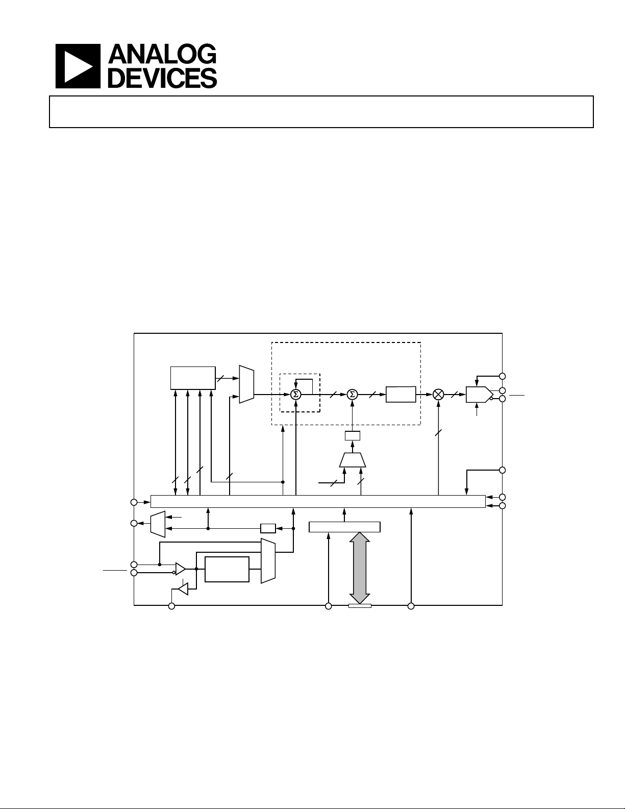
RAM
DDS CLOCK
RAM CONTROL
3
10
4×–20×
CLOCK
MULTIPLIER
DATA
32
32
I/O UPDATE
SYNC_CLK
REFCLK
REFCLK
1024 × 32
STATIC RAM
S
S
E
R
D
D
A
M
A
RAM DATA
R
32
0
M
U
X
OSCILLATOR/BUFFER
ENABLE
OUT
FUNCTIONAL BLOCK DIAGRAM
M
U
X
FREQUENCY
TUNING WORD
TIMING AND CONTROL LOGIC
SYNC
÷ 4
M
U
X
PHASE
ACCUMULATOR
–1
Z
RESET
PHASE
DDS CLOCK
ACCUMULATOR
RAM DATA <31:18>
CONTROL REGISTERS
SYSTEM
CLOCK
Direct Digital Synthesizer
PLL REFCLK multiplier (4× to 20×)
Internal oscillator, can be driven by a single crystal
Phase modulation capability
Multichip synchronization
APPLICATIONS
Agile VHF/UHF LO frequency synthesis
FM chirp source for radar and scanning systems
Nonlinear-shaped PSK/FSK modulator
Test and measurement equipment
DDS CORE
PHASE
OFFSET
Z
MUX
14
19 14
COS(X)
–1
PHASE
14
OFFSET
WORD
14
AD9953
SYSTEM
CLOCK
DAC
DAC_R
IOUT
IOUT
SYNC_IN
OSK
PWRDWNCTL
AD9953
SET
CRYSTAL OUT I/O PORTPS<1:0>
Rev. 0
Information furnished by Analog Devices is believed to be accurate and reliable.
However, no responsibility is assumed by Analog Devices for its use, nor for any
infringements of patents or other rights of third parties that may result from its use.
Specifications subject to change without notice. No license is granted by implication
or otherwise under any patent or patent rights of Analog Devices. Trademarks and
registered trademarks are the property of their respective owners.
Figure 1.
03357-0-001
RESET
One Technology Way, P.O. Box 9106, Norwood, MA 02062-9106, U.S.A.
Tel: 781.329.4700 www.analog.com
Fax: 781.326.8703 © 2004 Analog Devices, Inc. All rights reserved.

AD9953
TABLE OF CONTENTS
General Description ......................................................................... 3
Programming AD9953 Features............................................... 22
Electrical Specifications ................................................................... 4
Absolute Maximum Ratings............................................................ 6
Pin Configuration............................................................................. 7
Pin Function Descriptions .............................................................. 8
Typical Performance Characteristics ............................................. 9
Theory of Operation ...................................................................... 12
Component Blocks..................................................................... 12
Modes of Operation ................................................................... 19
REVISION HISTORY
Revision 0: Initial Version
Serial Port Operation................................................................. 25
Instruction Byte.......................................................................... 27
Serial Interface Port Pin Description....................................... 27
MSB/LSB Transfers .................................................................... 27
Suggested Application Circuits ..................................................... 29
Outline Dimensions....................................................................... 30
ESD Caution................................................................................ 30
Ordering Guide .......................................................................... 30
Rev. 0 | Page 2 of 32

AD9953
GENERAL DESCRIPTION
The AD9953 is a direct digital synthesizer (DDS) featuring a
14-bit DAC operating up to 400 MSPS. The AD9953 uses
advanced DDS technology, coupled with an internal high speed,
high performance DAC to form a digitally programmable,
complete high frequency synthesizer capable of generating a
frequency-agile analog output sinusoidal waveform at up to
200 MHz. The AD9953 includes an integrated 1024 × 32 static
RAM to support flexible frequency sweep capability in several
modes. The AD9953 is designed to provide fast frequency hopping and fine tuning resolution (32-bit frequency tuning word).
The frequency tuning and control words are loaded into the
AD9953 via a serial I/O port.
The AD9953 is specified to operate over the extended industrial
temperature range of –40°C to +105°C.
Rev. 0 | Page 3 of 32

AD9953
ELECTRICAL SPECIFICATIONS
Table 1. Unless otherwise noted, AVDD, DVDD = 1.8 V ± 5%, DVDD_I/O = 3.3 V ± 5%, R
Frequency = 20 MHz with REFCLK Multiplier Enabled at 20×. DAC Output Must Be Referenced to AVDD, Not AGND.
Parameter Temp Min Typ Max Unit
REF CLOCK INPUT CHARACTERISTICS
Frequency Range
REFCLK Multiplier Disabled FULL 1 400 MHz
REFCLK Multiplier Enabled at 4× FULL 20 100 MHz
REFCLK Multiplier Enabled at 20× FULL 4 20 MHz
Input Capacitance 25°C 3 pF
Input Impedance 25°C 1.5 kΩ
Duty Cycle 25°C 50 %
Duty Cycle with REFCLK Multiplier Enabled 25°C 35 65 %
REFCLK Input Power1 FULL –15 0 +3 dBm
DAC OUTPUT CHARACTERISTICS
Resolution 14 Bits
Full-Scale Output Current 25°C 5 10 15 mA
Gain Error 25°C –10 +10 %FS
Output Offset 25°C 0.6 µA
Differential Nonlinearity 25°C 1 LSB
Integral Nonlinearity 25°C 2 LSB
Output Capacitance 25°C 5 pF
Residual Phase Noise @ 1 kHz Offset, 40 MHz A
REFCLK Multiplier Enabled @ 20× 25°C –105 dBc/Hz
REFCLK Multiplier Enabled @ 4× 25°C –115 dBc/Hz
REFCLK Multiplier Disabled 25°C –132 dBc/Hz
Voltage Compliance Range 25°C AVDD – 0.5 AVDD + 0.5 V
Wideband SFDR
1 MHz to 10 MHz Analog Out 25°C 73 dBc
10 MHz to 40 MHz Analog Out 25°C 67 dBc
40 MHz to 80 MHz Analog Out 25°C 62 dBc
80 MHz to 120 MHz Analog Out 25°C 58 dBc
120 MHz to 160 MHz Analog Out 25°C 52 dBc
Narrow-Band SFDR
40 MHz Analog Out (±1 MHz) 25°C 87 dBc
40 MHz Analog Out (±250 kHz) 25°C 89 dBc
40 MHz Analog Out (±50 kHz) 25°C 91 dBc
40 MHz Analog Out (±10 kHz) 25°C 93 dBc
80 MHz Analog Out (±1 MHz) 25°C 85 dBc
80 MHz Analog Out (±250 kHz) 25°C 87 dBc
80 MHz Analog Out (±50 kHz) 25°C 89 dBc
80 MHz Analog Out (±10 kHz) 25°C 91 dBc
120 MHz Analog Out (±1 MHz) 25°C 83 dBc
120 MHz Analog Out (±250 kHz) 25°C 85 dBc
120 MHz Analog Out (±50 kHz) 25°C 87 dBc
120 MHz Analog Out (±10 kHz) 25°C 89 dBc
160 MHz Analog Out (±1 MHz) 25°C 81 dBc
160 MHz Analog Out (±250 kHz) 25°C 83 dBc
160 MHz Analog Out (±50 kHz) 25°C 85 dBc
160 MHz Analog Out (±10 kHz) 25°C 87 dBc
OUT
= 3.92 kΩ, External Reference Clock
SET
Rev. 0 | Page 4 of 32

AD9953
Parameter Temp Min Typ Max Unit
TIMING CHARACTERISTICS
Serial Control Bus
Maximum Frequency FULL 25 Mbps
Minimum Clock Pulse Width Low FULL 7 ns
Minimum Clock Pulse Width High FULL 7 ns
Maximum Clock Rise/Fall Time FULL 2 ns
Minimum Data Setup Time DVDD_I/O = 3.3 V FULL 3 ns
Minimum Data Setup Time DVDD_I/O = 1.8 V FULL 5 ns
Minimum Data Hold Time FULL 0 ns
Maximum Data Valid Time FULL 25 ns
Wake-Up Time2 FULL 1 ms
Minimum Reset Pulse Width High FULL 5 SYSCLK Cycles3
I/O UPDATE (PS0/PS1) to SYNC_CLK Setup Time DVDD_I/O = 3.3 V FULL 4 ns
I/O UPDATE (PS0/PS1) to SYNC_CLK Setup Time DVDD_I/O = 1.8 V FULL 6 ns
I/O UPDATE (PS0/PS1), SYNC_CLK Hold Time FULL 0 ns
Latency
I/O UPDATE (PS0/PS1) to Frequency Change Prop Delay 25°C 24 SYSCLK Cycles
I/O UPDATE (PS0/PS1) to Phase Offset Change Prop Delay 25°C 24 SYSCLK Cycles
I/O UPDATE (PS0/PS1) to Amplitude Change Prop Delay 25°C 16 SYSCLK Cycles
CMOS LOGIC INPUTS
Logic 1 Voltage @ DVDD_I/O (Pin 43) = 1.8 V 25°C 1.25 V
Logic 0 Voltage @ DVDD_I/O (Pin 43) = 1.8 V 25°C 0.6 V
Logic 1 Voltage @ DVDD_I/O (Pin 43) = 3.3 V 25°C 2.2 V
Logic 0 Voltage @ DVDD_I/O (Pin 43) = 3.3 V 25°C 0.8 V
Logic 1 Current 25°C 3 12 µA
Logic 0 Current 25°C 12 µA
Input Capacitance 25°C 2 pF
CMOS LOGIC OUTPUTS (1 mA Load) DVDD_I/O = 1.8 V
Logic 1 Voltage 25°C 1.35 V
Logic 0 Voltage 25°C 0.4 V
CMOS LOGIC OUTPUTS (1 mA Load) DVDD_I/O = 3.3 V
Logic 1 Voltage 25°C 2.8 V
Logic 0 Voltage 25°C 0.4 V
POWER CONSUMPTION (AVDD = DVDD = 1.8 V)
Single-Tone Mode 25°C 162 171 mW
Rapid Power-Down Mode 25°C 150 160 mW
Full-Sleep Mode 25°C 20 27 mW
SYNCHRONIZATION FUNCTION4
Maximum SYNC Clock Rate (DVDD_I/O = 1.8 V) 25°C 62.5 MHz
Maximum SYNC Clock Rate (DVDD_I/O = 3.3 V) 25°C 100 MHz
SYNC_CLK Alignment Resolution5 25°C ±1 SYSCLK Cycles
1
To achieve the best possible phase noise, the largest amplitude clock possible should be used. Reducing the clock input amplitude will reduce the phase noise
performance of the device.
2
Wake-up time refers to the recovery from analog power-down modes (see the Power-Down Functions of the AD9953 section). The longest time required is for the
reference clock multiplier PLL to relock to the reference. The wake-up time assumes there is no capacitor on DACBP and that the recommended PLL loop filter values
are used.
3
SYSCLK cycle refers to the actual clock frequency used on-chip by the DDS. If the reference clock multiplier is used to multiply the external reference clock frequency,
the SYSCLK frequency is the external frequency multiplied by the reference clock multiplication factor. If the reference clock multiplier is not used, the SYSCLK
frequency is the same as the external reference clock frequency.
4
SYNC_CLK = ¼ SYSCLK rate. For SYNC_CLK rates ≥ 50 MHz, the high speed sync enable bit, CFR2<11>, should be set.
5
This parameter indicates that the digital synchronization feature cannot overcome phase delays (timing skew) between system clock rising edges. If the system clock
edges are aligned, the synchronization function should not increase the skew between the two edges.
Rev. 0 | Page 5 of 32
AD9953
ABSOLUTE MAXIMUM RATINGS
Table 2.
Parameter Rating
Maximum Junction Temperature 150°C
DVDD_I/O (Pin 43) 4 V
AVDD, DVDD 2 V
Digital Input Voltage (DVDD_I/O = 3.3 V) –0.7 V to +5.25 V
Digital Input Voltage (DVDD_I/O = 1.8 V) –0.7 V to +2.2 V
Digital Output Current 5 mA
Storage Temperature –65°C to +150°C
Operating Temperature –40°C to +105°C
Lead Temperature (10 sec Soldering) 300°C
θJA 38°C/W
θJC 15°C/W
Stresses above those listed under Absolute Maximum Ratings
may cause permanent damage to the device. This is a stress
rating only and functional operation of the device at these or
any other conditions above those indicated in the operational
section of this specification is not implied. Exposure to absolute
maximum rating conditions for extended periods may affect
device reliability.
DIGITAL
INPUTS
DVDD_I/O
INPUT
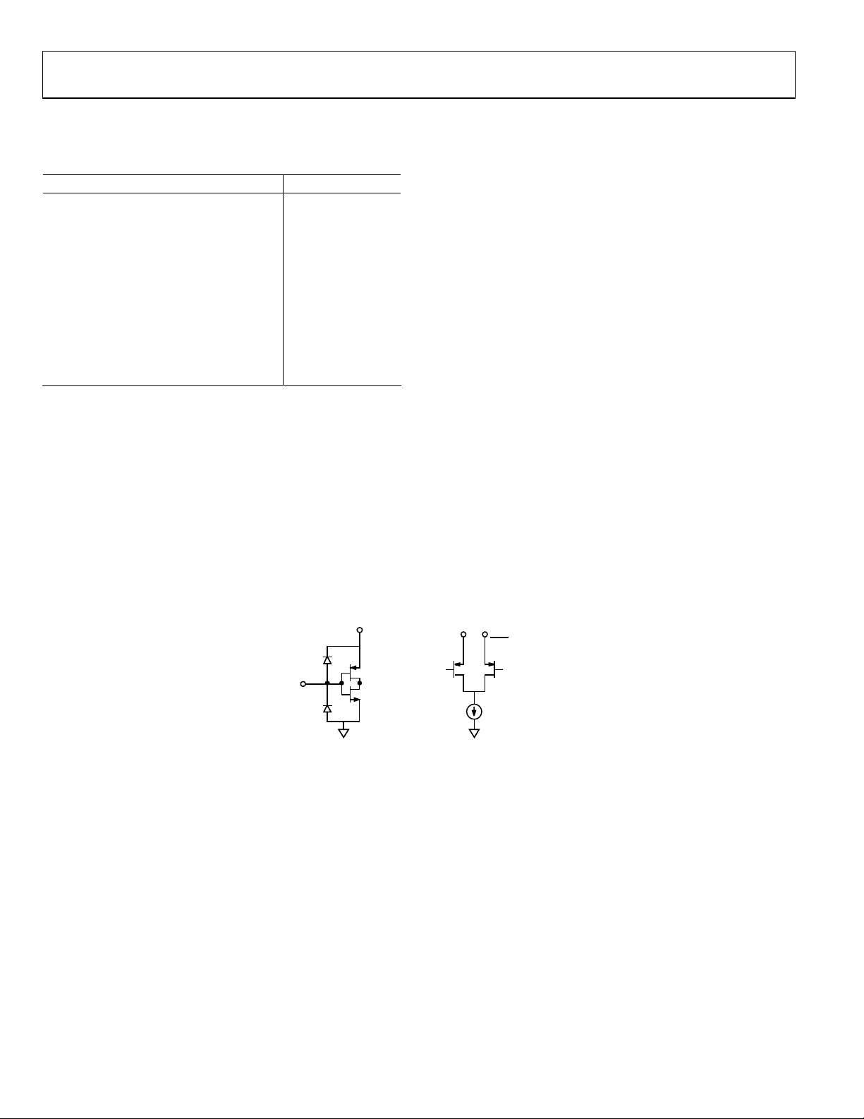
AVOID OVERDRIVING
DIGITAL INPUTS.
FORWARD BIASING
ESD DIODES MAY
COUPLE DIGITAL NOISE
ONTO POWER PINS.
Figure 2. Equivalent Input and Output Circuits
DAC OUT PUTS
IOUT
MUST TERMINATE
OUTPUTS TO AVDD. DO
NOT EXCEED THE
OUTPUT VOLTAGE
COMPLIANCE RATING.
IOUT
03374-0-032
Rev. 0 | Page 6 of 32
AD9953
PIN CONFIGURATION
OSK
PS1
PS0
SYNC_CLK
SYNC_IN
48 47 464544
DVDD_I/O
43
SCLK
DGND
SDIO
4241403938 37
SDOCSIOSYNC
I/O UPDATE
DVDD
DGND
AVDD
AGND
AVDD
AGND
OSC/REFCLK
OSC/REFCLK
CRYSTAL OUT
CLKMODESELECT
LOOP_FILTER
1
2
3
4
5
6
7
8
9
10
11
12
13 15 16 17 18 19 20 21 22 23 24
14
AVDD
AGND
AGND
AD9953
TOP VIEW
(Not to Scale)
AVDD
AGND
AVDD
AVDD
IOUT
IOUT
AGND
DACBP
SET
DAC_R
RESET
36
PWRDWNCTL
35
DVDD
34
DGND
33
AGND
32
AGND
31
AGND
30
AVDD
29
AGND
28
AVDD
27
AGND
26
AVDD
25
03357-0-002
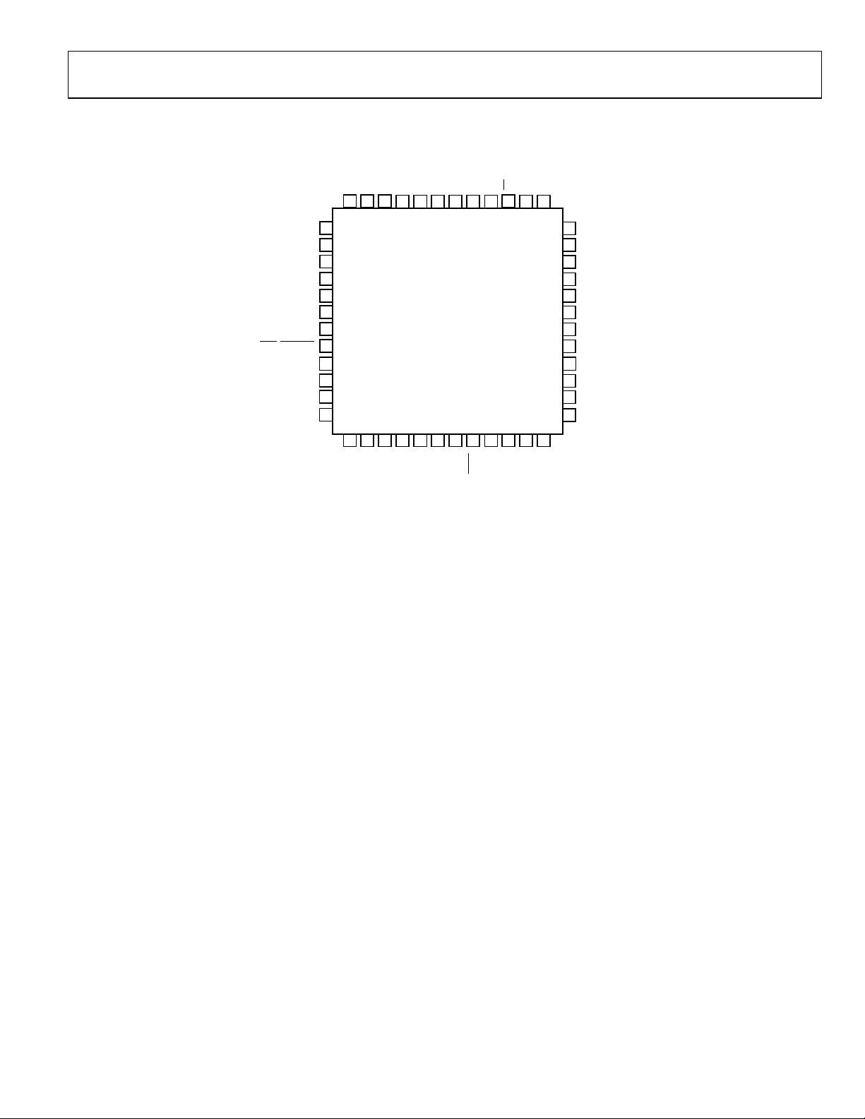
Figure 3. 48-Lead TQFP/EP
Note that the exposed paddle on the bottom of the package forms an electrical connection for the DAC and must be attached to
analog ground. Note that Pin 43, DVDD_I/O, can be powered to 1.8 V or 3.3 V; however, the DVDD pins (Pin 2 and Pin 34) can only
be powered to 1.8 V.
Rev. 0 | Page 7 of 32
AD9953
PIN FUNCTION DESCRIPTIONS
Table 3. 48-Lead TQFP/EP
Pin No. Mnemonic I/O Description
1 I/O UPDATE I
2, 34 DVDD I Digital Power Supply Pins (1.8 V).
3, 33, 42 DGND I Digital Power Ground Pins.
4, 6, 13,
16, 18, 19,
25, 27, 29
5, 7, 14,
15, 17, 22,
26, 32
8
9 OSC/REFCLK I
10 CRYSTAL OUT O Output of the Oscillator Section.
11 CLKMODESELECT I
12 LOOP_FILTER I
20
21 IOUT O DAC Output. Should be biased through a resistor to AVDD, not AGND.
23 DACBP I DAC Biasline Decoupling Pin.
24 DAC_R
35 PWRDWNCTL I Input Pin Used as an External Power-Down Control (see Table 10 for details).
36 RESET I
37 IOSYNC I
38 SDO O
39
40 SCLK I This pin functions as the serial data clock for I/O operations.
41 SDIO I/O
43 DVDD_I/O I Digital Power Supply (for I/O Cells Only, 3.3 V).
44 SYNC_IN I
45 SYNC_CLK O Clock Output Pin that Serves as a Synchronizer for External Hardware.
46 OSK I
47, 48 PS0, PS1 I
<49> AGND I
AVDD I Analog Power Supply Pins (1.8 V).
AGND I Analog Power Ground Pins.
/REFCLK
OSC
IOUT
I
SET
CS
The rising edge transfers the contents of the internal buffer memory to the I/O registers. This pin
must be set up and held around the SYNC_CLK output signal.
I
Complementary Reference Clock/Oscillator Input. When the REFCLK port is operated in singleended mode, REFCLK
Reference Clock/Oscillator Input. See Clock Input section for details on the OSCILLATOR/REFCLK
operation.
Control Pin for the Oscillator Section. When high, the oscillator section is enabled. When low, the
oscillator section is bypassed.
This pin provides the connection for the external zero compensation network of the REFCLK
multiplier’s PLL loop filter. The network consists of a 1 kΩ resistor in series with a 0.1 µF capacitor
tied to AVDD.
O Complementary DAC Output. Should be biased through a resistor to AVDD, not AGND.
A resistor (3.92 kΩ nominal) connected from AGND to DAC_R
for the DAC.
Active High Hardware Reset Pin. Assertion of the RESET pin forces the AD9953 to the initial state,
as described in the I/O port register map.
Asynchronous Active High Reset of the Serial Port Controller. When high, the current I/O
operation is immediately terminated, enabling a new I/O operation to commence once IOSYNC is
returned low. If unused, ground this pin; do not allow this pin to float.
When operating the I/O port as a 3-wire serial port, this pin serves as the serial data output. When
operated as a 2-wire serial port, this pin is unused and can be left unconnected.
I This pin functions as an active low chip select that allows multiple devices to share the I/O bus.
When operating the I/O port as a 3-wire serial port, this pin serves as the serial data input only.
When operated as a 2-wire serial port, this pin is the bidirectional serial data pin.
Input Signal Used to Synchronize Multiple AD9953s. This input is connected to the SYNC_CLK
output of a master AD9953.
Input Pin Used to Control the Direction of the Shaped On-Off Keying Function when
Programmed for Operation. OSK is synchronous to the SYNC_CLK pin. When OSK is not
programmed, this pin should be tied to DGND.
Input pin used to select one of the four internal profiles. Profile <1:0> are synchronous to the
SYNC_CLK pin. Any change in these inputs transfers the contents of the internal buffer memory
to the I/O registers (sends an internal I/O UPDATE).
The exposed paddle on the bottom of the package is a ground connection for the DAC and must
be attached to AGND in any board layout.
should be decoupled to AVDD with a 0.1 µF capacitor.
establishes the reference current
SET
Rev. 0 | Page 8 of 32
AD9953
K
K
K
K
K
K
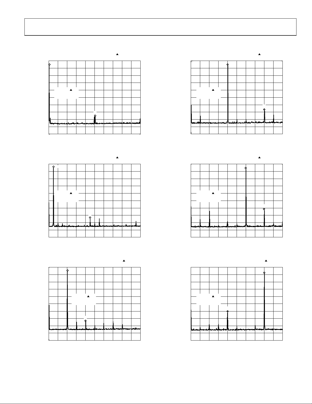
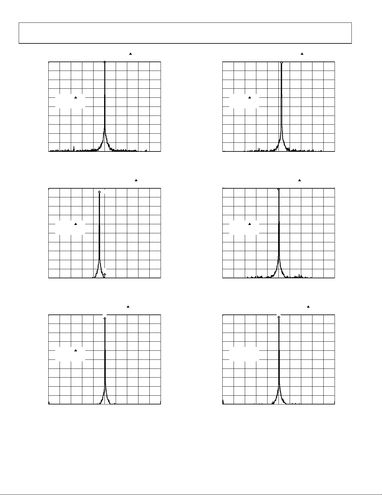
TYPICAL PERFORMANCE CHARACTERISTICS
PEA
LOG
10dB/
W1 S2
S3 FC
AA
PEA
LOG
10dB/
W1 S2
S3 FC
AA
PEA
LOG
10dB/
W1 S2
S3 FC
AA
REF 0dBm
0
1R
–10
–20
–30
–40
–50
–60
–70
–80
–90
–100
CENTER 100MHz
#RES BW 3kHz
Figure 4. F
REF 0dBm
0
–10
–20
–30
–40
–50
–60
–70
–80
–90
–100
CENTER 100MHz
#RES BW 3kHz
Figure 5. F
REF 0dBm
0
–10
–20
–30
–40
–50
–60
–70
–80
–90
–100
CENTER 100MHz
#RES BW 3kHz
Figure 6. F
ATTEN 10dB
MARKER
100.000000MHz
–70.68dB
1
VBW 3kHz
= 1 MHz FCLK = 400 MSPS, WBSFDR
OUT
ATTEN 10dB
1R
MARKER
80.000000MHz
–69.12dB
1
VBW 3kHz
= 10 MHz, FCLK = 400 MSPS, WBSFDR
OUT
ATTEN 10dB
1R
MARKER
40.000000MHz
–68.44dB
1
VBW 3kHz
= 40 MHz, FCLK = 400 MSPS, WBSFDR
OUT
MKR1 98.0MHz
–70.68dB
SWEEP 55.56 s (401 PTS)
SWEEP 55.56 s (401 PTS)
SWEEP 55.56 s (401 PTS)
SPAN 200MHz
MKR1 80.0MHz
–69.12dB
SPAN 200MHz
MKR1 0Hz
–68.44dB
SPAN 200MHz
03374-0-016
03374-0-017
03374-0-018
PEA
LOG
10dB/
W1 S2
S3 FC
AA
PEA
LOG
10dB/
W1 S2
S3 FC
AA
PEA
LOG
10dB/
W1 S2
S3 FC
AA
REF 0dBm
0
–10
–20
–30
–40
–50
–60
–70
–80
–90
–100
CENTER 100MHz
#RES BW 3kHz
Figure 7. F
REF 0dBm
0
–10
–20
–30
–40
–50
–60
–70
–80
–90
–100
CENTER 100MHz
#RES BW 3kHz
Figure 8. F
REF 0dBm
0
–10
–20
–30
–40
–50
–60
–70
–80
–90
–100
CENTER 100MHz
#RES BW 3kHz
Figure 9. F
ATTEN 10dB
1R
MARKER
80.000000MHz
–61.55dB
VBW 3kHz
= 80 MHz FCLK = 400 MSPS, WBSFDR
OUT
ATTEN 10dB
MARKER
40.000000MHz
–56.2dB
VBW 3kHz
= 120 MHz, FCLK = 400 MSPS, WBSFDR
OUT
ATTEN 10dB
MARKER
80.000000MHz
–53.17dB
= 160 MHz, FCLK = 400 MSPS, WBSFDR
OUT
1
VBW 3kHz
MKR1 80.0MHz
–61.55dB
1
1R
SPAN 200MHz
MKR1 40.0MHz
–56.2dB
1
SPAN 200MHz
MKR1 0Hz
–53.17dB
1R
SPAN 200MHz
SWEEP 55.56 s (401 PTS)
SWEEP 55.56 s (401 PTS)
SWEEP 55.56 s (401 PTS)
03374-0-019
03374-0-020
03374-0-021
Rev. 0 | Page 9 of 32
AD9953
K
K
K
K
K
K
REF –4dBm
0
PEA
LOG
–10
10dB/
–20
–30
–40
–50
–60
W1 S2
–70
S3 FC
AA
–80
–90
ST
–100
CENTER 1.105MHz
#RES BW 30Hz
Figure 10. F
REF 0dBm
0
PEA
LOG
–10
10dB/
–20
–30
–40
–50
–60
W1 S2
–70
S3 FC
AA
–80
–90
–100
CENTER 10MHz
#RES BW 30Hz
Figure 11. F
REF 0dBm
0
PEA
LOG
–10
10dB/
–20
–30
–40
–50
–60
W1 S2
–70
S3 FC
AA
–80
–90
–100
CENTER 39.9MHz
#RES BW 30Hz
Figure 12. F
ATTEN 10dB
MARKER
1.105000MHz
–5.679dBm
= 1.1 MHz, FCLK = 400 MSPS, NBSFDR, ±1 MHz
OUT
ATTEN 10dB
MARKER
40.000000MHz
–56.2dB
= 10 MHz, FCLK = 400 MSPS, NBSFDR, ±1 MHz
OUT
ATTEN 10dB
MARKER
39.905000MHz
–5.347dBm
= 39.9 MHz, FCLK = 400 MSPS, NBSFDR, ±1 MHz
OUT
1
VBW 30Hz
1R
1
VBW 30Hz
1
VBW 30Hz
MKR1 1.105MHz
SWEEP 199.2 s (401 PTS)
MKR1 85kHz
SWEEP 199.2 s (401 PTS)
MKR1 39.905MHz
SWEEP 199.2 s (401 PTS)
–5.679dBm
SPAN 2MHz
–93.01dB
SPAN 2MHz
–5.347dBm
SPAN 2MHz
03374-0-022
03374-0-023
03374-0-024
REF –4dBm
PEA
LOG
10dB/
W1 S2
S3 FC
AA
ST
Figure 13. F
REF –4dBm
PEA
LOG
10dB/
W1 S2
S3 FC
AA
ST
Figure 14. F
REF –4dBm
PEA
LOG
10dB/
W1 S2
S3 FC
AA
ST
Figure 15. F
0
–10
–20
–30
MARKER
–40
80.301000MHz
–6.318dBm
–50
–60
–70
–80
–90
–100
CENTER 80.25MHz
#RES BW 30Hz
0
–10
–20
–30
MARKER
–40
120.205000MHz
–6.825dBm
–50
–60
–70
–80
–90
–100
CENTER 120.2MHz
#RES BW 30Hz
0
–10
–20
–30
CENTER
–40
160.5000000MHz
–50
–60
–70
–80
–90
–100
CENTER 160.5MHz
#RES BW 30Hz
MKR1 80.301MHz
ATTEN 10dB
= 80.3 MHz, FCLK = 400 MSPS, NBSFDR, ±1 MHz
OUT
ATTEN 10dB
= 120.2 MHz, FCLK = 400 MSPS, NBSFDR, ±1 MHz
OUT
ATTEN 10dB
= 160 MHz, FCLK = 400 MSPS, NBSFDR, ±1 MHz
OUT
VBW 30Hz
VBW 30Hz
VBW 30Hz
1
SWEEP 199.2 s (401 PTS)
1
SWEEP 199.2 s (401 PTS)
1
SWEEP 199.2 s (401 PTS)
–6.318dBm
SPAN 2MHz
MKR1 120.205MHz
–6.825dBm
SPAN 2MHz
MKR1 600kHz
–0.911dB
SPAN 2MHz
03374-0-025
03374-0-026
03374-0-027
Rev. 0 | Page 10 of 32
 Loading...