12-Bit CCD Signal Processor with
FEATURES
New AD9949A supports CCD line length > 4096 pixels
Correlated double sampler (CDS)
0 dB to 18 dB pixel gain amplifier (PxGA®)
6 dB to 42 dB 10-bit variable gain amplifier (VGA)
12-bit, 36 MSPS analog-to-digital converter (ADC)
Black level clamp with variable level control
Complete on-chip timing driver
Precision Timing™ core with < 600 ps resolution
On-chip 3 V horizontal and RG drivers
40-lead LFCSP package
APPLICATIONS
Digital still cameras
High speed digital imaging applications
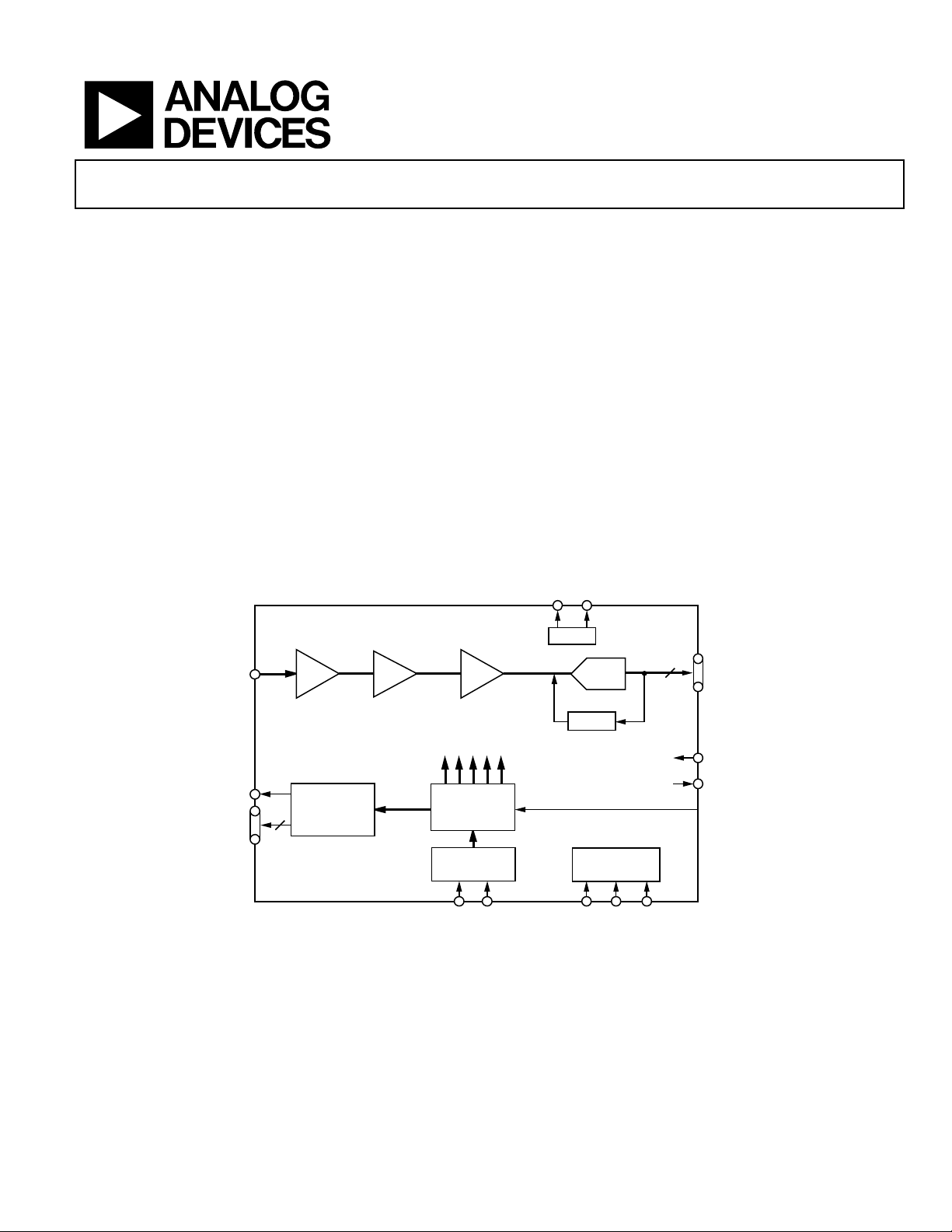
FUNCTIONAL BLOCK DIAGRAM
Precision Timing
Core
AD9949
GENERAL DESCRIPTION
The AD9949 is a highly integrated CCD signal processor for
digital still camera applications. Specified at pixel rates of up to
36 MHz, the AD9949 consists of a complete analog front end
with A/D conversion, combined with a programmable timing
driver. The Precision Timing core allows adjustment of high
speed clocks with < 600 ps resolution.
The analog front end includes black level clamping, CDS,
PxGA, VGA, and a 36 MSPS, 12-bit ADC. The timing driver
provides the high speed CCD clock drivers for RG and H1 to
H4. Operation is programmed using a 3-wire serial interface.
Packaged in a space-saving, 40-lead LFCSP package, the
AD9949 is specified over an operating temperature range of
−20°C to +85°C.
REFT REFB
6dB TO 42dB
INTERNAL
CLOCKS
PRECISION
GENERATOR
HD VD
CCDIN
RG
H1 TO H4
4
AD9949
CDS
HORIZONTAL
DRIVERS
0dB TO 18dB
PxGA
Rev. B
Information furnished by Analog Devices is believed to be accurate and reliable.
However, no responsibility is assumed by Analog Devices for its use, nor for any
infringements of patents or other rights of third parties that may result from its use.
Specifications subject to change without notice. No license is granted by implication
or otherwise under any patent or patent rights of Analog Devices. Trademarks and
registered trademarks are the property of their respective owners.
VGA
TIMING
CORE
SYNC
Figure 1.
V
REF
12-BIT
ADC
CLAMP
INTERNAL
REGISTERS
SL
One Technology Way, P.O. Box 9106, Norwood, MA 02062-9106, U.S.A.
Tel: 781.329.4700
Fax: 781.326.8703 © 2004 Analog Devices, Inc. All rights reserved.
www.analog.com
12
DOUT
HBLK
CLP/PBLK
CLI
SDATASCK
03751-001

AD9949
TABLE OF CONTENTS
Specifications..................................................................................... 3
Individual HBLK Sequences..................................................... 21
General Specifications ................................................................. 3
Digital Specifications ................................................................... 3
Analog Specifications................................................................... 4
Timing Specifications .................................................................. 5
Absolute Maximum Ratings............................................................ 6
Thermal Characteristics .............................................................. 6
ESD Caution.................................................................................. 6
Pin Configuration and Function Descriptions............................. 7
Terminology ...................................................................................... 8
Equivalent Input/Output Circuits.................................................. 9
Typical Performance Characteristics ........................................... 10
System Overview ............................................................................ 11
H-Counter Behavior ..................................................................11
Serial Interface Timing .................................................................. 12
Complete Register Listing ............................................................. 13
Generating Special HBLK Patterns.............................................. 23
Horizontal Sequence Control................................................... 23
External HBLK Signal................................................................ 23
H-Counter Synchronization ..................................................... 24
Power-Up Procedure...................................................................... 25
Recommended Power-Up Sequence ....................................... 25
Analog Front End Description and Operation .......................... 26
DC Restore .................................................................................. 26
Correlated Double Sampler ...................................................... 26
PxGA............................................................................................ 26
Variable Gain Amplifier ............................................................ 29
ADC ............................................................................................. 29
Optical Black Clamp.................................................................. 29
Digital Data Outputs.................................................................. 29
Applications Information.............................................................. 30
Precision Timing High Speed Timing Generation...................... 18
Timing Resolution...................................................................... 18
High Speed Clock Programmability........................................ 18
H-Driver and RG Outputs ........................................................ 19
Digital Data Outputs.................................................................. 19
Horizontal Clamping and Blanking............................................. 21
Individual CLPOB and PBLK Sequences................................ 21
REVISION HISTORY
11/04—Data Sheet Changed from Rev. A to Rev. B
Changes to Ordering Guide.......................................................... 35
9/04—Data Sheet Changed from Rev. 0 to Rev. A
Changes to Features.......................................................................... 1
Changes to Analog Specifications .................................................. 4
Changes to Terminology Section.................................................... 9
Added H-Counter Behavior Section............................................ 12
Changes to Table 7.......................................................................... 14
Circuit Configuration................................................................ 30
Grounding and Decoupling Recommendations.................... 30
Driving the CLI Input................................................................ 31
Horizontal Timing Sequence Example.................................... 31
Outline Dimensions....................................................................... 34
Ordering Guide .......................................................................... 34
Changes to Table 12 ....................................................................... 17
Changes to Table 15 ....................................................................... 17
Changes to H-Counter Sync Section........................................... 24
Changes to Recommended Power-Up Sequence Section ......... 25
Changes to Ordering Guide.......................................................... 35
5/03—Revision 0: Initial Version
Rev. B | Page 2 of 36

AD9949
SPECIFICATIONS
GENERAL SPECIFICATIONS
Table 1.
Parameter Min Typ Max Unit
TEMPERATURE RANGE
Operating −20 +85 °C
Storage −65 +150 °C
MAXIMUM CLOCK RATE 36 MHz
POWER SUPPLY VOLTAGE
AVDD, TCVDD (AFE, Timing Core) 2.7 3.0 3.6 V
HVDD (H1 to H4 Drivers) 2.7 3.0 3.6 V
RGVDD (RG Driver) 2.7 3.0 3.6 V
DRVDD (D0 to D11 Drivers) 2.7 3.0 3.6 V
DVDD (All Other Digital) 2.7 3.0 3.6 V
POWER DISSIPATION
36 MHz, HVDD = RGVDD = 3 V, 100 pF H1 to H4 Loading1 320 mW
Total Shutdown Mode 1 mW
1
The total power dissipated by the HVDD supply may be approximated using the equation
Total HVDD Power = (CLOAD x HVDD x Pixel Frequency) x HVDD x (Number of H – Outputs Used)
Reducing the H-loading, using only two of the outputs, and/or using a lower HVDD supply, reduces the power dissipation.
DIGITAL SPECIFICATIONS
T
to T
MIN
Table 2.
Parameter Symbol Min Typ Max Unit
LOGIC INPUTS
High Level Input Voltage VIH 2.1 V
Low Level Input Voltage VIL 0.6 V
High Level Input Current IIH 10 µA
Low Level Input Current IIL 10 µA
Input Capacitance CIN 10 pF
LOGIC OUTPUTS
High Level Output Voltage, IOH = 2 mA VOH 2.2 V
Low Level Output Voltage, IOL = 2 mA VOL 0.5 V
CLI INPUT
High Level Input Voltage
Low Level Input Voltage V
RG AND H-DRIVER OUTPUTS
High Level Output Voltage
Low Level Output Voltage VOL 0.5 V
Maximum Output Current (Programmable) 30 mA
Maximum Load Capacitance 100 pF
, AVDD = DVDD = DRVDD = HVDD = RGVDD = 2.7 V, CL = 20 pF, unless otherwise noted.
MAX
(TCVDD/2 + 0.5 V) V
(RGVDD – 0.5 V and HVDD – 0.5 V) VOH 2.2 V
1.85 V
IH–CLI
0.85 V
IL–CLI
Rev. B | Page 3 of 36

AD9949
ANALOG SPECIFICATIONS
T
to T
MIN
Table 3.
Parameter Min Typ Max Unit Notes
CDS
Gain 0 dB
Allowable CCD Reset Transient1 500 mV
Maximum Input Range before Saturation1 1.0 V p-p
Maximum CCD Black Pixel Amplitude1 ±50 mV
PIXEL GAIN AMPLIFIER (P×GA)
Gain Control Resolution 256 Steps
Gain Monotonicity
VARIABLE GAIN AMPLIFIER (VGA)
Maximum Input Range 1.0 V p-p
Maximum Output Range 2.0 V p-p
Gain Control Resolution 1024 Steps
Gain Monotonicity Guaranteed
Gain Range
BLACK LEVEL CLAMP
Clamp Level Resolution 256 Steps
Clamp Level Measured at ADC output
A/D CONVERTER
Resolution 12 Bits
Differential Nonlinearity (DNL) −1.0 ±0.5 +1.0 LSB
No Missing Codes Guaranteed
Integral Nonlinearity (INL) 8 LSB
Full-Scale Input Voltage 2.0 V
VOLTAGE REFERENCE
Reference Top Voltage (REFT) 2.0 V
Reference Bottom Voltage (REFB) 1.0 V
SYSTEM PERFORMANCE Specifications include entire signal chain
VGA Gain Accuracy
Peak Nonlinearity, 500 mV Input Signal 0.15 0.6 % 12 dB gain applied
Total Output Noise 0.8 LSB rms AC grounded input, 6 dB gain applied
Power Supply Rejection (PSR) 50 dB Measured with step change on supply
1
Input signal characteristics defined as follows:
, AVDD = DVDD = 3.0 V, f
MAX
= 36 MHz, typical timing specifications, unless otherwise noted.
CLI
Minimum Gain 0 dB
Maximum Gain 18 dB
Minimum Gain (VGA Code 0) 6 dB
Maximum Gain (VGA Code 1023) 42 dB
Minimum Clamp Level (0) 0 LSB
Maximum Clamp Level (255) 255 LSB
Minimum Gain (Code 0) 5.0 5.5 6.0 dB
Maximum Gain (Code 1023) 40.5 41.5 42.5 dB
500mV TYP
RESET TRANSIENT
50mV MAX
OPTICAL BLACK PIXEL
1V MAX
INPUT SIGNAL RANGE
03751-002
Rev. B | Page 4 of 36

AD9949
TIMING SPECIFICATIONS
CL = 20 pF, f
Table 4.
Parameter Symbol Min Typ Max Unit
MASTER CLOCK (CLI) (See Figure 16)
CLI Clock Period t
CLI High/Low Pulse Width t
Delay from CLI to Internal Pixel Period Position t
CLPOB PULSE WIDTH (PROGRAMMABLE)1 t
SAMPLE CLOCKS (See Figure 18)
SHP Rising Edge to SHD Rising Edge tS1 12.5 13.9 ns
DATA OUTPUTS (See Figure 19 and Figure 20)
Output Delay From Programmed Edge tOD 6 ns
Pipeline Delay 11 Cycles
SERIAL INTERFACE (SERIAL TIMING SHOWN IN Figure 14 and Figure 15)
Maximum SCK Frequency f
SL to SCK Setup Time tLS 10 ns
SCK to SL Hold Time tLH 10 ns
SDATA Valid to SCK Rising Edge Setup tDS 10 ns
SCK Falling Edge to SDATA Valid Hold tDH 10 ns
SCK Falling Edge to SDATA Valid Read tDV 10 ns
1
Minimum CLPOB pulse width is for functional operation only. Wider typical pulses are recommended to achieve low noise clamp reference.
= 36 MHz, unless otherwise noted.
CLI
27.8 ns
CLI
11.2 13.9 16.6 ns
ADC
6 ns
CLIDLY
2 20 Pixels
COB
10 MHz
SCLK
Rev. B | Page 5 of 36
AD9949
ABSOLUTE MAXIMUM RATINGS
Table 5.
With
Parameter
AVDD and TCVDD AVSS −0.3 V to +3.9 V
HVDD and RGVDD
DVDD and DRVDD
Any VSS Any VSS −0.3 V to +0.3 V
Digital Outputs DRVSS −0.3 V to DRVDD + 0.3 V
CLPOB/PBLK and HBLK DVSS −0.3 V to DVDD + 0.3 V
SCK, SL, and SDATA DVSS −0.3 V to DVDD + 0.3 V
RG RGVSS −0.3 V to RGVDD + 0.3 V
H1 to H4 HVSS −0.3 V to HVDD + 0.3 V
REFT, REFB, and CCDIN AVSS −0.3 V to AVDD + 0.3 V
Junction Temperature 150°C
Lead Temperature (10 s) 300°C
Respect to Rating
HVSS,
RGVSS
DVSS,
DRVSS
−0.3 V to +3.9 V
−0.3 V to +3.9 V
Stresses above those listed under Absolute Maximum Ratings
may cause permanent damage to the device. This is a stress
rating only; functional operation of the device at these or any
other conditions above those listed in the operational sections
of this specification is not implied. Exposure to absolute maximum rating conditions for extended periods may affect device
reliability.
THERMAL CHARACTERISTICS
Thermal Resistance
40-Lead LFCSP Package: θ
1
θJA is measured using a 4-layer PCB with the exposed paddle soldered to the
board.
= 27°C/W1.
JA
ESD CAUTION
ESD (electrostatic discharge) sensitive device. Electrostatic charges as high as 4000 V readily accumulate
on the human body and test equipment and can discharge without detection. Although this product features
proprietary ESD protection circuitry, permanent damage may occur on devices subjected to high energy electrostatic discharges. Therefore, proper ESD precautions are recommended to avoid performance degradation
or loss of functionality.
Rev. B | Page 6 of 36

AD9949
PIN CONFIGURATION AND FUNCTION DESCRIPTIONS
HVSS
HVDD
SL
SCK
SDI
31
30
REFB
REFT
29
28
AVSS
27
CCDIN
26
AVDD
25
CLI
TCVDD
24
23
TCVSS
RGVDD
22
RG
21
H4
H3
RGVSS
03751-003
DRVSS
DRVDD
D0 (LSB)
CLP/PBLK
HBLK
DVDD
DVSSHDVD
403938373635343332
1
D1
D2
D3
D4
D5
D6
D7
D8
10
2
3
4
5
6
7
8
9
PIN 1
INDICATOR
AD9949
TOP VIEW
11
121314151617181920
H2
H1
D9
D10
(MSB) D11
Figure 2. Pin Configuration
Table 6. Pin Function Descriptions
Pin No. Mnemonic Type1 Description
1 to 4 D1 to D4 DO Data Outputs
5 DRVSS P Digital Driver Ground
6 DRVDD P Digital Driver Supply
7 to 13 D5 to D11 DO Data Outputs (D11 is MSB)
14 H1 DO CCD Horizontal Clock 1
15 H2 DO CCD Horizontal Clock 2
16 HVSS P H1 to H4 Driver Ground
17 HVDD P H1 to H4 Driver Supply
18 H3 DO CCD Horizontal Clock 3
19 H4 DO CCD Horizontal Clock 4
20 RGVSS P RG Driver Ground
21 RG DO CCD Reset Gate Clock
22 RGVDD P RG Driver Supply
23 TCVSS P Analog Ground for Timing Core
24 TCVDD P Analog Supply for Timing Core
25 CLI DI Master Clock Input
26 AVDD P Analog Supply for AFE
27 CCDIN AI Analog Input for CCD Signal (Connect through Series 0.1 µF Capacitor)
28 AVSS P Analog Ground for AFE
29 REFT AO Reference Top Decoupling (Decouple with 1.0 µF to AVSS)
30 REFB AO Reference Bottom Decoupling (Decouple with 1.0 µF to AVSS)
31 SL DI 3-Wire Serial Load
32 SDI DI 3-Wire Serial Data Input
33 SCK DI 3-Wire Serial Clock
34 VD DI Vertical Sync Pulse
35 HD DI Horizontal Sync Pulse
36 DVSS P Digital Ground
37 DVDD P Digital Supply
38 HBLK DI Optional HBLK Input
39 CLP/PBLK DO CLPOB or PBLK Output
40 D0 DO Data Output LSB
1
Type: AI = Analog Input, AO = Analog Output, DI = Digital Input, DO = Digital Output, P = Power.
Rev. B | Page 7 of 36

AD9949
TERMINOLOGY
Differential Nonlinearity (DNL)
An ideal ADC exhibits code transitions that are exactly 1 LSB
apart. DNL is the deviation from this ideal value. Thus, every
code must have a finite width. No missing codes guaranteed to
12-bit resolution indicates that all 4096 codes, respectively, must
be present over all operating conditions.
Integral Nonlinearity (INL)
INL is the deviation of each individual code measured from a
true straight line from zero to full scale. The point used as zero
scale occurs 0.5 LSB before the first code transition. Positive full
scale is defined as a level 1 LSB and 0.5 LSB beyond the last
code transition. The deviation is measured from the middle of
each particular output code to the true straight line.
Peak Nonlinearity
Peak nonlinearity, a full signal chain specification, refers to the
peak deviation of the output of the AD9949 from a straight line.
The point used as zero scale occurs 0.5 LSB before the first code
transition. Positive full scale is defined as a level 1 LSB and
0.5 LSB beyond the last code transition. The deviation is
measured from the middle of each particular output code to the
straight line reference. The error is then expressed as a
percentage of the 2 V ADC full-scale signal. The input signal is
appropriately gained up to fill the ADC’s full-scale range.
Tot a l O ut p ut Noi s e
The rms output noise is measured using histogram techniques.
The standard deviation of the ADC output codes is calculated
in LSB and represents the rms noise level of the total signal
chain at the specified gain setting. The output noise can be converted to an equivalent voltage, using the relationship
n
1 LSB = (ADC full scale/2
where n is the bit resolution of the ADC. For the AD9949,
1 LSB is approximately 0.488 mV.
Power Supply Rejection (PSR)
The PSR is measured with a step change applied to the supply
pins. The PSR specification is calculated from the change in the
data outputs for a given step change in the supply voltage.
codes)
Rev. B | Page 8 of 36
AD9949
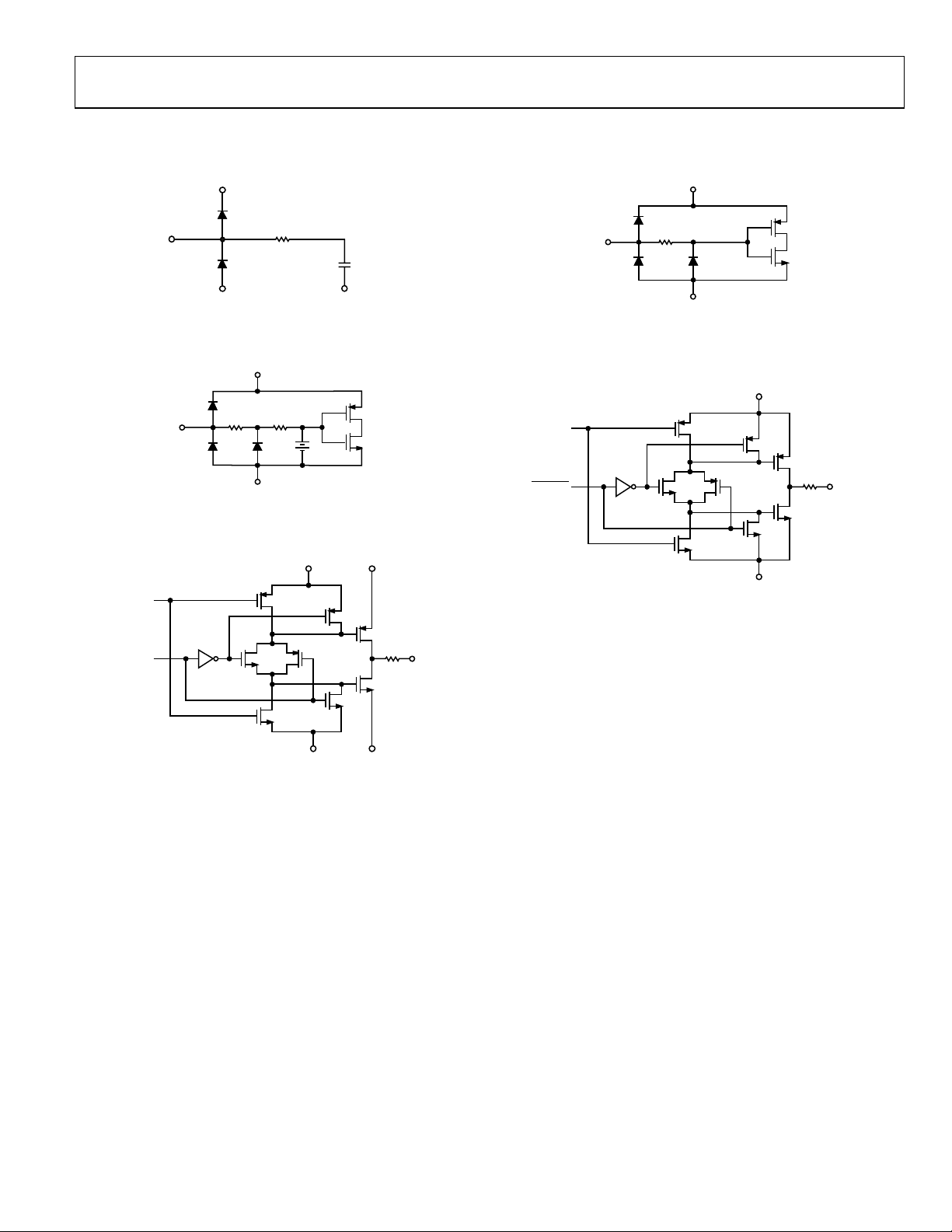
EQUIVALENT INPUT/OUTPUT CIRCUITS
DATA
CLI
AVDD
R
AVSS
Figure 3. CCDIN (Pin 27)
AVDD
330Ω
25kΩ
+
1.4V
AVSS
Figure 4. CLI (Pin 25)
DVSS
AVSS
03751-004
03751-005
DRVDD
DVDD
330Ω
DVSS
03751-007
Figure 6. Digital Inputs (Pins 31 to 35, 38)
HVDD OR RGVDD
DATA
ENABLE DOUT
HVSS OR RGVSS
03751-008
Figure 7. H1 to H4 and RG (Pins 14 to 15, 18 to 19, 21)
THREE-STATE DOUT
DVSS DRVSS
Figure 5. Data Outputs D0 to D11 (Pins 1 to 4, 7 to 13, 40)
03751-006
Rev. B | Page 9 of 36
AD9949
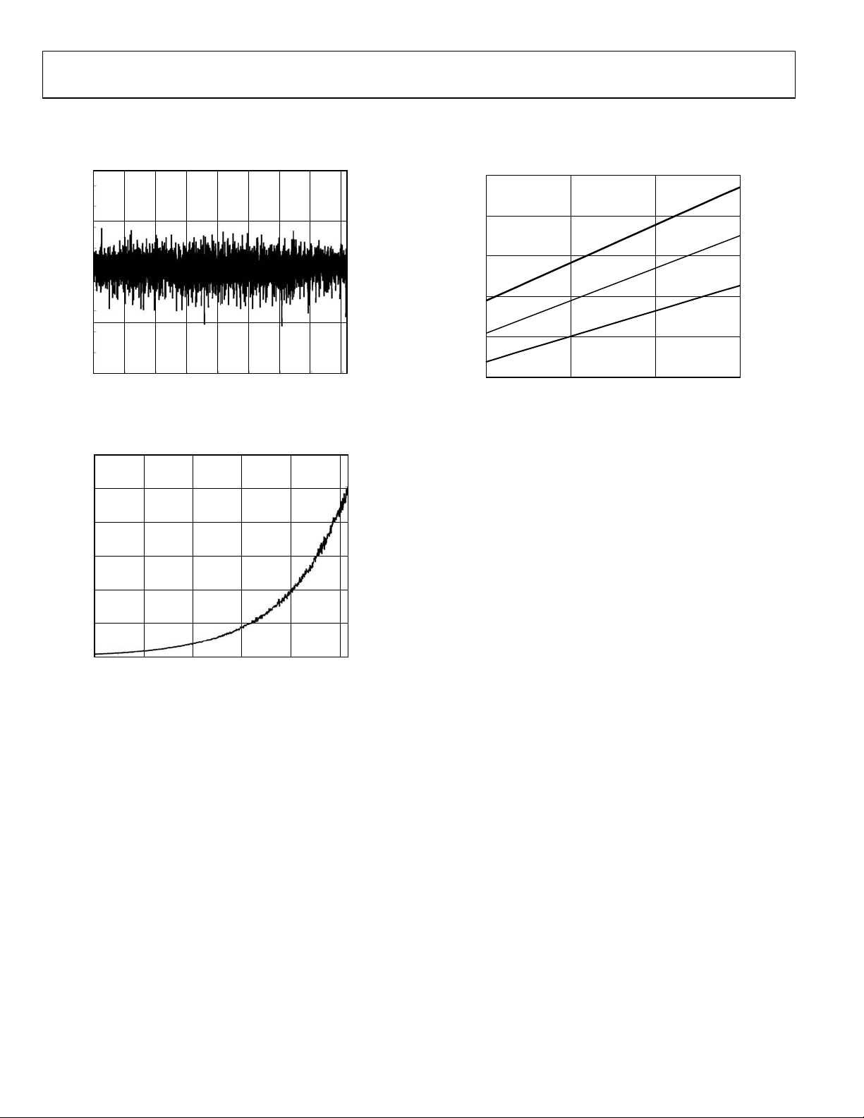
TYPICAL PERFORMANCE CHARACTERISTICS
1.0
400
0.5
0
DNL (LSB)
–0.5
–1.0
ADC OUTPUT CODE
40000 500 1000 1500 2000 2500 3000 3500
03751-009
Figure 8. Typical D NL
48
40
32
24
16
OUTPUT NOISE (LSB)
8
350
300
VDD = 3.3V
250
POWER DISSIPATION (mW)
200
150
= 3.0V
V
DD
= 2.7V
V
DD
SAMPLE RATE (MHz)
3618 24 30
03751-011
Figure 10. Power Curves
0
VGA GAIN CODE (LSB)
10000 200 400 600 800
03751-010
Figure 9. Output Noise vs. VGA Gain
Rev. B | Page 10 of 36
AD9949
SYSTEM OVERVIEW
CCD
V-DRIVER
H1 TO H4, RG
CCDIN
Figure 11. Typical Application
V1 TO Vx, VSG1 TO VSGx, SUBCK
AD9949
INTEGRATED
AFE + TD
SERIAL
INTERFACE
DOUT
HD, VD
CLI
DIGITAL IMAGE
PROCESSING
ASIC
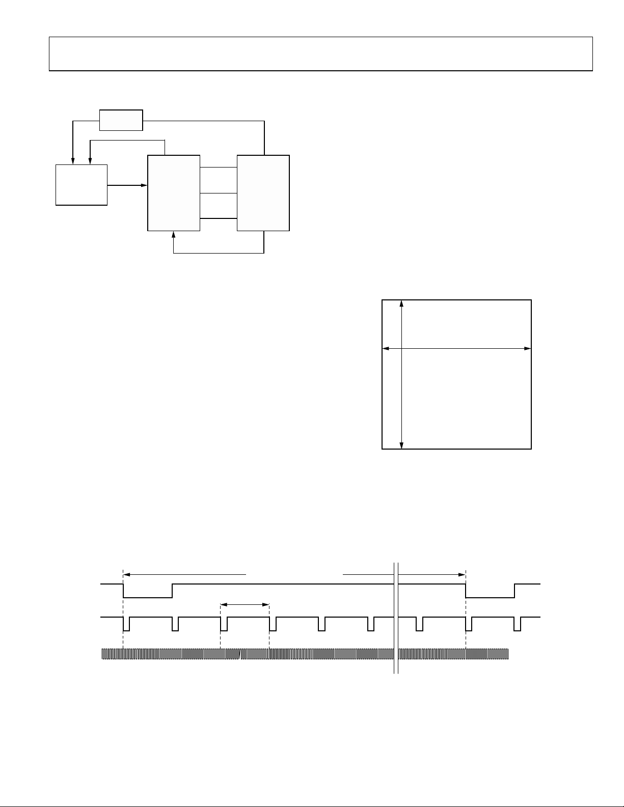
Figure 11 shows the typical system application diagram for the
AD9949. The CCD output is processed by the AD9949’s AFE
circuitry, which consists of a CDS, a PxGA, a VGA, a black level
clamp, and an ADC. The digitized pixel information is sent to
the digital image processor chip where all postprocessing and
compression occurs. To operate the CCD, CCD timing
parameters are programmed into the AD9949 from the image
processor through the 3-wire serial interface. From the system
master clock, CLI, provided by the image processor, the
AD9949 generates the high speed CCD clocks and all internal
AFE clocks. All AD9949 clocks are synchronized with VD and
HD. The AD9949’s horizontal pulses (CLPOB, PBLK, and
HBLK) are programmed and generated internally.
The H-drivers for H1 to H4 and RG are included in the
AD9949, allowing these clocks to be directly connected to the
CCD. The H-drive voltage of 3 V is supported in the AD9949.
Figure 12 shows the horizontal and vertical counter dimensions
for the AD9949. All internal horizontal clocking is programmed
using these dimensions to specify line and pixel locations.
H-COUNTER BEHAVIOR
When the maximum horizontal count of 4096 pixels is
exceeded, the H-counter in the AD9949 rolls over to zero and
continues counting. It is, therefore, recommended that the
maximum counter value not be exceeded.
However, the newer AD9949A version behaves differently. In
the AD9949A, the internal H-counter holds at its maximum
count of 4095 instead of rolling over. This feature allows the
AD9949A to be used in applications containing a line length
greater than 4096 pixels. Although no programmable values for
03751-012
the horizontal blanking or clamping are available beyond pixel
4095, the H, RG, and AFE clocking continues to operate,
sampling the remaining pixels on the line.
MAXIMUM FIELD DIMENSIONS
12-BIT HORIZONTAL = 4096 PIXELS MAX
12-BIT VERTICAL = 4096 LINES MAX
03751-013
Figure 12. Vertical and Horizontal Counters
VD
HD
CLI
MAX VD LENGTH IS 4095 LINES
MAX HD LENGTH IS 4095 PIXELS
Figure 13. Maximum VD/HD Dimensions
Rev. B | Page 11 of 36
03751-014
 Loading...