10-Bit CCD Signal Processor with
FEATURES
Correlated Double Sampler (CDS)
0 dB to 18 dB Pixel Gain Amplifier (
PxGA
®
)
6 dB to 42 dB 10-Bit Variable Gain Amplifier (VGA)
10-Bit 25 MSPS A/D Converter
Black Level Clamp with Variable Level Control
Complete On-Chip Timing Driver
Precision Timing Core with 800 ps Resolution
On-Chip 3 V Horizontal and RG Drivers
40-Lead LFCSP Package
APPLICATIONS
Digital Still Cameras
High Speed Digital Imaging Applications
Precision Timing
™
Core
AD9948
GENERAL DESCRIPTION
The AD9948 is a highly integrated CCD signal processor for
digital still camera applications. Specified at pixel rates of up to
25 MHz, the AD9948 consists of a complete analog front end
with A/D conversion, combined with a programmable timing
driver. The Precision Timing core allows adjustment of high
speed clocks with 800 ps resolution.
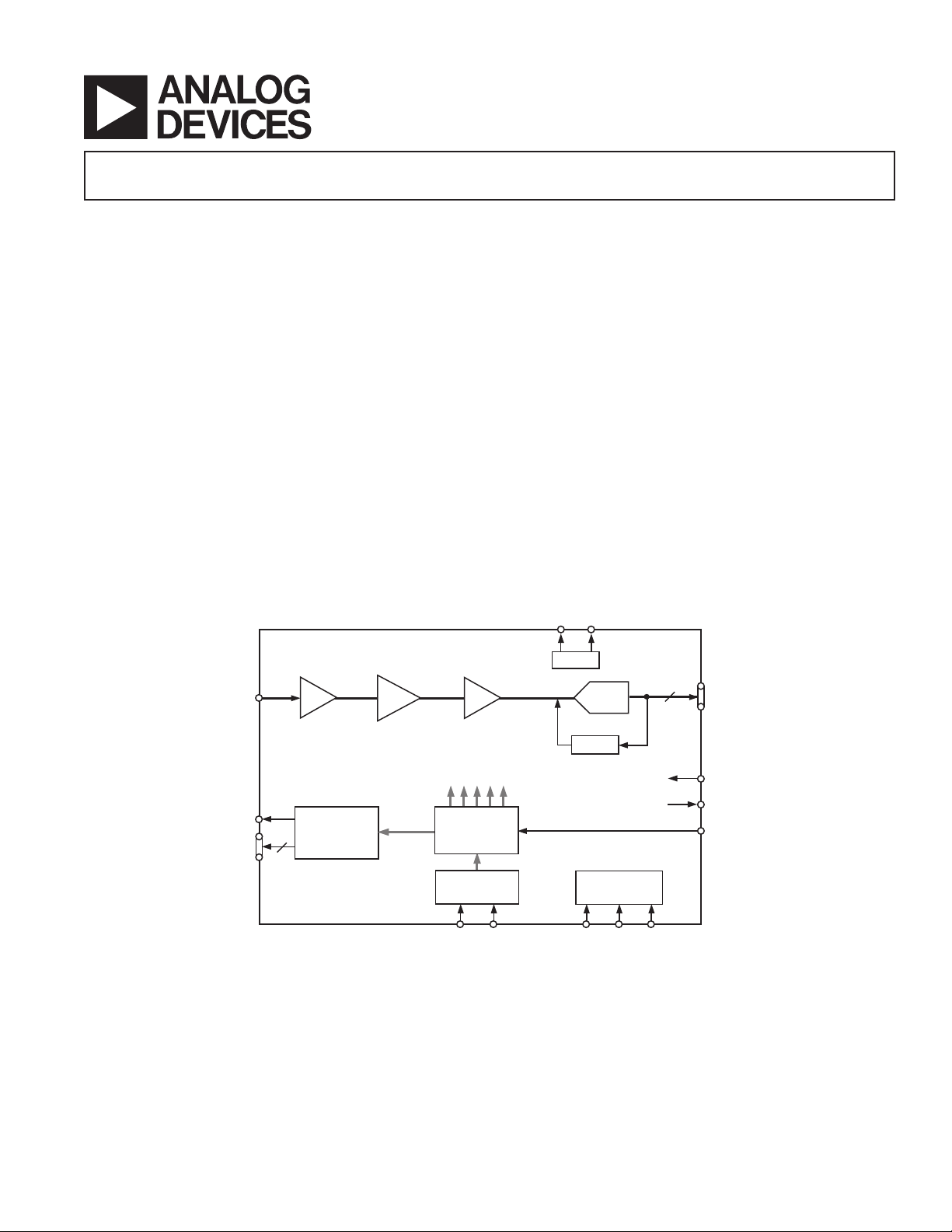
The analog front end includes black level clamping, CDS, PxGA,
VGA, and a 25 MHz 10-bit A/D converter. The timing driver
provides the high speed CCD clock drivers for RG and H1–H4.
Operation is programmed using a 3-wire serial interface.
Packaged in a space-saving 40-lead LFCSP package, the
AD9948 is specified over an operating temperature range of
–20°C to +85°C.
CCDIN
RG
H1–H4
4
AD9948
CDS
HORIZONTAL
DRIVERS
FUNCTIONAL BLOCK DIAGRAM
REFB
REFT
V
0dB TO 18dB
PxGA
6dB TO 42dB
VGA
INTERNAL
CLOCKS
PRECISION
TIMING
CORE
SYNC
GENERATOR
HD VD
REF
CLAMP
SL
10-BIT
ADC
INTERNAL
REGISTERS
10
DOUT
HBLK
CLP/PBLK
CLI
SDATASCK
REV. 0
Information furnished by Analog Devices is believed to be accurate and
reliable. However, no responsibility is assumed by Analog Devices for its
use, nor for any infringements of patents or other rights of third parties that
may result from its use. No license is granted by implication or otherwise
under any patent or patent rights of Analog Devices. Trademarks and
registered trademarks are the property of their respective companies.
One Technology Way, P.O. Box 9106, Norwood, MA 02062-9106, U.S.A.
Tel: 781/329-4700 www.analog.com
Fax: 781/326-8703 © 2003 Analog Devices, Inc. All rights reserved.

AD9948–SPECIFICATIONS
GENERAL SPECIFICATIONS
Parameter Min Typ Max Unit
TEMPERATURE RANGE
Operating –20 +85 °C
Storage –65 +150 °C
MAXIMUM CLOCK RATE 25 MHz
POWER SUPPLY VOLTAGE
AVDD, TCVDD (AFE, Timing Core) 2.7 3.0 3.6 V
HVDD (H1–H4 Drivers) 2.7 3.0 3.6 V
RGVDD (RG Driver) 2.7 3.0 3.6 V
DRVDD (D0–D9 Drivers) 2.7 3.0 3.6 V
DVDD (All Other Digital) 2.7 3.0 3.6 V
POWER DISSIPATION
25 MHz, HVDD = RGVDD = 3 V, 100 pF H1–H4 Loading* 220 mW
Total Shutdown Mode 1 mW
*The total power dissipated by the HVDD supply may be approximated using the equation
Total HVDD Power C HVDD Pixel Frequency HVDD Number of H Outputs Used
Reducing the H-loading, using only two of the outputs, and/or using a lower HVDD supply will reduce the power dissipation.
Specifications subject to change without notice.
=×× ×× −()()
LOAD
DIGITAL SPECIFICATIONS
(T
to T
MIN
, AVDD = DVDD = DRVDD = HVDD = RGVDD = 2.7 V, CL = 20 pF, unless otherwise noted.)
MAX
Parameter Symbol Min Typ Max Unit
LOGIC INPUTS
High Level Input Voltage V
Low Level Input Voltage V
High Level Input Current I
Low Level Input Current I
Input Capacitance C
IH
IL
IH
IL
IN
2.1 V
0.6 V
10 µA
10 µA
10 pF
LOGIC OUTPUTS
High Level Output Voltage, IOH = 2 mA V
Low Level Output Voltage, IOL = 2 mA V
OH
OL
2.2 V
0.5 V
CLI INPUT
High Level Input Voltage
(TCVDD/2 + 0.5 V) V
Low Level Input Voltage V
IH–CLI
IL–CLI
1.85 V
0.85 V
RG AND H-DRIVER OUTPUTS
High Level Output Voltage
(RGVDD – 0.5 V and HVDD – 0.5 V) V
Low Level Output Voltage V
OH
OL
2.2 V
0.5 V
Maximum Output Current (Programmable) 30 mA
Maximum Load Capacitance 100 pF
Specifications subject to change without notice.
REV. 0–2–
AD9948
(T
to T
, AVDD = DVDD = 3.0 V, f
MAX
ANALOG SPECIFICATIONS
MIN
unless otherwise noted.)
Parameter Min Typ Max Unit Notes
CDS
Gain 0 dB
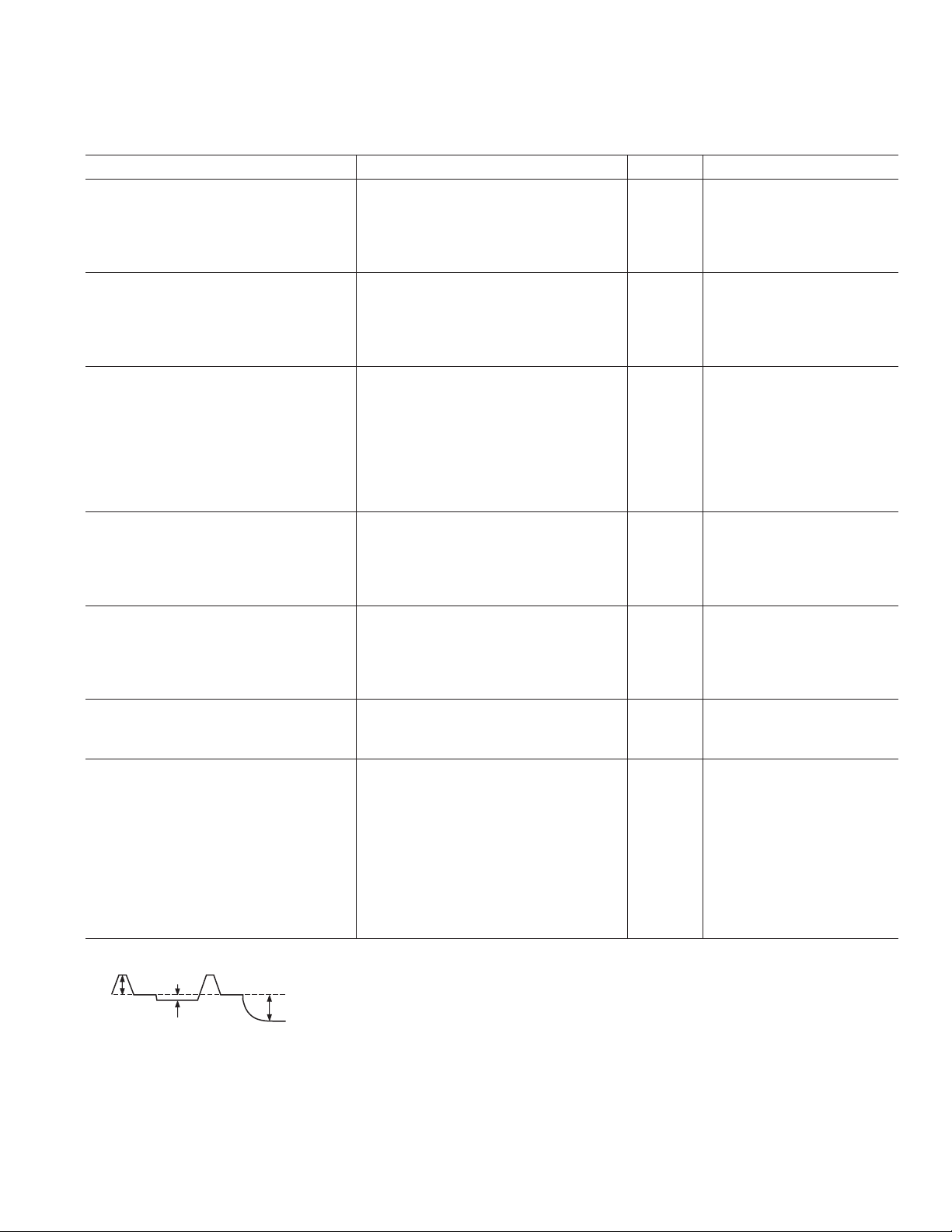
Allowable CCD Reset Transient* 500 mV
Max Input Range before Saturation* 1.0 V p-p
Max CCD Black Pixel Amplitude* ±50 mV
PIXEL GAIN AMPLIFIER (PxGA)
Gain Control Resolution 256 Steps
Gain Monotonicity
Min Gain 0 dB
Max Gain 18 dB
VARIABLE GAIN AMPLIFIER (VGA)
Max Input Range 1.0 V p-p
Max Output Range 2.0 V p-p
Gain Control Resolution 1024 Steps
Gain Monotonicity Guaranteed
Gain Range
Min Gain (VGA Code 0) 6 dB
Max Gain (VGA Code 1023) 42 dB
BLACK LEVEL CLAMP
Clamp Level Resolution 256 Steps
Clamp Level Measured at ADC output
Min Clamp Level (0) 0 LSB
Max Clamp Level (255) 63.75 LSB
A/D CONVERTER
Resolution 10 Bits
Differential Nonlinearity (DNL) –1.0 ± 0.5 +1.0 LSB
No Missing Codes Guaranteed
Full-Scale Input Voltage 2.0 V
VOLTAGE REFERENCE
Reference Top Voltage (REFT) 2.0 V
Reference Bottom Voltage (REFB) 1.0 V
SYSTEM PERFORMANCE Specifications include entire
VGA Gain Accuracy
Min Gain (Code 0) 5.0 5.5 6.0 dB
Max Gain (Code 1023) 40.5 41.5 42.5 dB
Peak Nonlinearity, 500 mV Input Signal 0.2 % 12 dB gain applied
Total Output Noise 0.25 LSB rms AC grounded input, 6 dB
Power Supply Rejection (PSR) 50 dB Measured with step change
*Input signal characteristics defined as follows:
= 25 MHz, Typical Timing Specifications,
CLI
signal chain
gain applied
on supply
500mV TYP
RESET TRANSIENT
Specifications subject to change without notice.
50mV MAX
OPTICAL BLACK PIXEL
1V MAX
INPUT SIGNAL RANGE
REV. 0
–3–
AD9948
TIMING SPECIFICATIONS
(CL = 20 pF, f
= 25 MHz, Serial Timing in Figure 3, unless otherwise noted.)
CLI
Parameter Symbol Min Typ Max Unit
MASTER CLOCK (CLI) (See Figure 4)
CLI Clock Period t
CLI High/Low Pulsewidth t
CLI
ADC
40 ns
16 20 24 ns
Delay from CLI to Internal Pixel
Period Position t
CLPOB Pulsewidth (Programmable)* t
CLIDLY
COB
220 Pixels
6ns
SAMPLE CLOCKS (See Figure 6)
SHP Rising Edge to SHD Rising Edge t
S1
17 20 ns
DATA OUTPUTS (See Figures 7a and 7b)
Output Delay From Programmed Edge t
OD
6ns
Pipeline Delay 11 Cycles
SERIAL INTERFACE
Maximum SCK Frequency f
SL to SCK Setup Time t
SCK to SL Hold Time t
SDATA Valid to SCK Rising Edge Setup t
SCK Falling Edge to SDATA Valid Hold t
SCK Falling Edge to SDATA Valid Read t
*Minimum CLPOB pulsewidth is for functional operation only. Wider typical pulses are recommended to achieve low noise clamp reference.
Specifications subject to change without notice.
SCLK
LS
LH
DS
DH
DV
10 MHz
10 ns
10 ns
10 ns
10 ns
10 ns
ABSOLUTE MAXIMUM RATINGS*
With
Parameter Respect To Min Max Unit
AVDD, TCVDD AVSS –0.3 +3.9 V
HVDD, RGVDD HVSS, RGVSS –0.3 +3.9 V
DVDD, DRVDD DVSS, DRVSS –0.3 +3.9 V
Any VSS Any VSS –0.3 +0.3 V
Digital Outputs DRVSS –0.3 DRVDD + 0.3 V
CLPOB/PBLK, HBLK DVSS –0.3 DVDD + 0.3 V
SCK, SL, SDATA DVSS –0.3 DVDD + 0.3 V
RG RGVSS –0.3 RGVDD + 0.3 V
H1–H4 HVSS –0.3 HVDD + 0.3 V
REFT, REFB, CCDIN AVSS –0.3 AVDD + 0.3 V
Junction Temperature 150 °C
Lead Temperature (10 sec) 300 °C
*Stresses above those listed under Absolute Maximum Ratings may cause permanent damage to the device. This is a stress
rating only; functional operation of the device at these or any other conditions above those listed in the operational sections
of this specification is not implied. Exposure to absolute maximum rating conditions for extended periods may affect
device reliability.
ORDERING GUIDE
Temperature Package Package
Model Range Description Option
AD9948KCP –20°C to +85°C LFCSP CP-40
AD9948KCPRL –20°C to +85°C LFCSP CP-40
THERMAL CHARACTERISTICS
Thermal Resistance
40-Lead LFCSP Package
= 27°C/W*
JA
*
is measured using a 4-layer PCB with the exposed paddle
JA
soldered to the board.
AD9948KCPZ* –20°C to +85°C LFCSP CP-40
AD9948KCPZRL* –20°C to +85°C LFCSP CP-40
*This is a lead free product.
CAUTION
ESD (electrostatic discharge) sensitive device. Electrostatic charges as high as 4000 V readily
accumulate on the human body and test equipment and can discharge without detection. Although
the AD9948 features proprietary ESD protection circuitry, permanent damage may occur on
devices subjected to high energy electrostatic discharges. Therefore, proper ESD precautions are
recommended to avoid performance degradation or loss of functionality.
REV. 0–4–
PIN CONFIGURATION
40 NC
38 HBLK
37 DVDD
36 DVSS
35 HD
34 VD
32 SDI
39 CLP/PBLK
33 SCK
31 SL
AD9948
NC 1
(LSB) D0 2
D1 3
D2 4
DRVSS 5
DRVDD 6
D3 7
D4 8
D5 9
D6 10
PIN 1
IDENTIFIER
D7 11
D8 12
AD9948
TOP VIEW
H1 14
H2 15
HVSS 16
(MSB) D9 13
H3 18
HVDD 17
30 REFB
29 REFT
28 AVSS
27 CCDIN
26 AVDD
25 CLI
24 TCVDD
23 TCVSS
22 RGVDD
21 RG
H4 19
RGVSS 20
PIN FUNCTION DESCRIPTIONS
Pin No. Mnemonic Type* Description
2–4 D0–D2 DO Data Outputs (D0 is LSB)
5 DRVSS P Digital Driver Ground
6 DRVDD P Digital Driver Supply
7–13 D3–D9 DO Data Outputs (D9 is MSB)
14 H1 DO CCD Horizontal Clock 1
15 H2 DO CCD Horizontal Clock 2
16 HVSS P H1–H4 Driver Ground
17 HVDD P H1–H4 Driver Supply
18 H3 DO CCD Horizontal Clock 3
19 H4 DO CCD Horizontal Clock 4
20 RGVSS P RG Driver Ground
21 RG DO CCD Reset Gate Clock
22 RGVDD P RG Driver Supply
23 TCVSS P Analog Ground for Timing Core
24 TCVDD P Analog Supply for Timing Core
25 CLI DI Master Clock Input
26 AVDD P Analog Supply for AFE
27 CCDIN AI Analog Input for CCD Signal (Connect through Series 0.1 µF Capacitor)
28 AVSS P Analog Ground for AFE
29 REFT AO Reference Top Decoupling (Decouple with 1.0 µF to AVSS)
30 REFB AO Reference Bottom Decoupling (Decouple with 1.0 µF to AVSS)
31 SL DI 3-Wire Serial Load
32 SDI DI 3-Wire Serial Data Input
33 SCK DI 3-Wire Serial Clock
34 VD DI Vertical Sync Pulse
35 HD DI Horizontal Sync Pulse
36 DVSS P Digital Ground
37 DVDD P Digital Supply
38 HBLK DI Optional HBLK Input
39 CLP/PBLK DO CLPOB or PBLK Output
1, 40 NC Not Internally Connected
*Type: AI = Analog Input, AO = Analog Output, DI = Digital Input, DO = Digital Output, P = Power.
REV. 0
–5–
AD9948
TERMINOLOGY
Differential Nonlinearity (DNL)
An ideal ADC exhibits code transitions that are exactly 1 LSB
apart. DNL is the deviation from this ideal value. Thus every
code must have a finite width. No missing codes guaranteed to
10-bit resolution indicates that all 1024 codes, respectively,
must be present over all operating conditions.
Peak Nonlinearity
Peak nonlinearity, a full signal chain specification, refers to the
peak deviation of the output of the AD9948 from a true straight
line. The point used as zero scale occurs 0.5 LSB before the
first code transition. Positive full scale is defined as a level 1 LSB
and 0.5 LSB beyond the last code transition. The deviation is
measured from the middle of each particular output code to the
true straight line. The error is then expressed as a percentage of
the 2 V ADC full-scale signal. The input signal is always appropriately gained up to fill the ADC’s full-scale range.
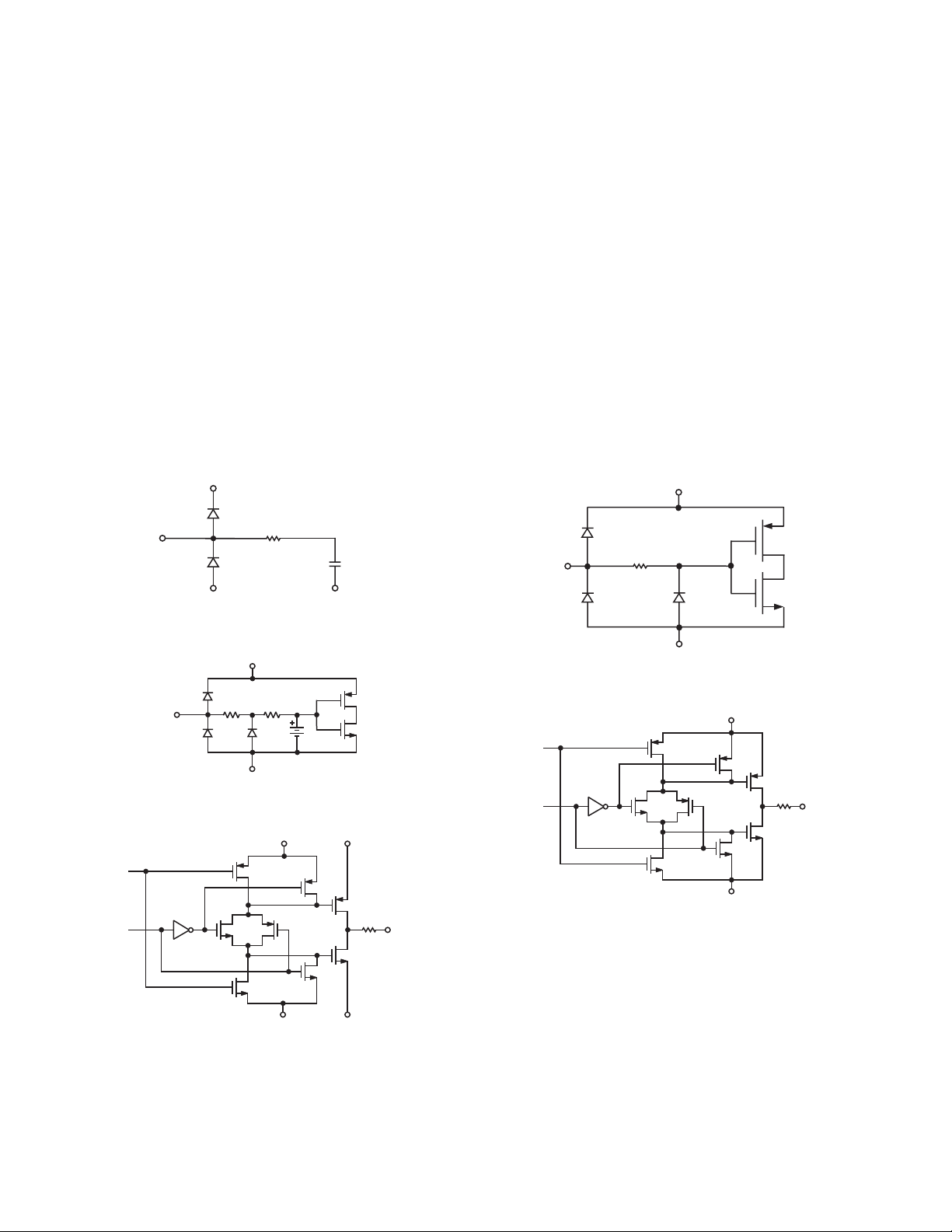
EQUIVALENT CIRCUITS
AVDD
R
Total Output Noise
The rms output noise is measured using histogram techniques.
The standard deviation of the ADC output codes is calculated in
LSB, and represents the rms noise level of the total signal chain
at the specified gain setting. The output noise can be converted
to an equivalent voltage, using the relationship
12
LSB (ADC full scale/ codes)=
n
where n is the bit resolution of the ADC. For the AD9948,
1LSB is approximately 1.95 mV.
Power Supply Rejection (PSR)
The PSR is measured with a step change applied to the supply
pins. The PSR specification is calculated from the change in the
data outputs for a given step change in the supply voltage.
DVD D
330
AVSS
AVSS
Circuit 1. CCDIN (Pin 27)
AVDD
330
CLI
25k
1.4V
AVSS
Circuit 2. CLI (Pin 25)
DVSS DRVDD
DATA
THREE-
STATE
DVSS DRVSS
Circuit 3. Data Outputs D0–D9 (Pins 2–4, 7–13)
DOUT
DVSS
Circuit 4. Digital Inputs (Pins 31–35, 38)
HVDD or RGVDD
DATA
ENABLE
HVSS or RGVSS
Circuit 5. H1–H4 and RG (Pins 14, 15, 18, 19, 21)
OUTPUT
REV. 0–6–
1.0
0.5
0
DNL (LSB)
–0.5
Typical Performance Characteristics–AD9948
–1.0
0
200 600 800
400
ADC OUTPUT CODE
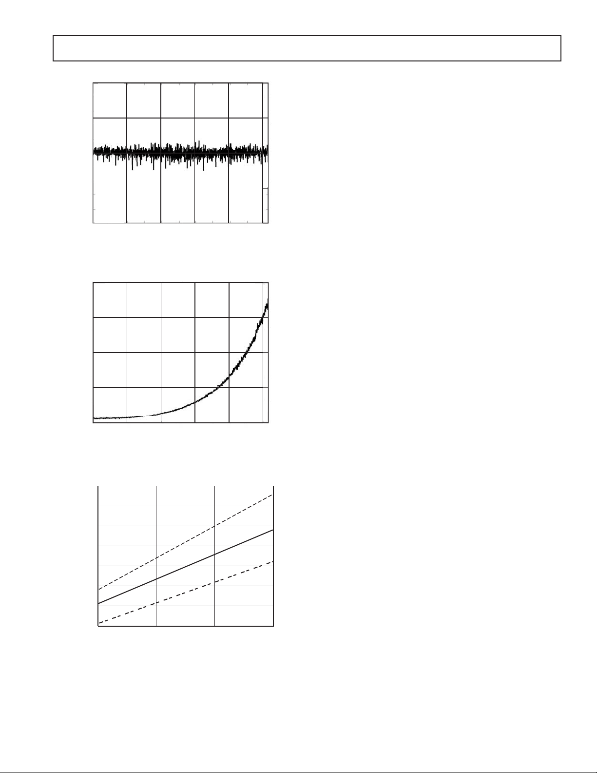
TPC 1. Typical DNL
10
7.5
5.0
OUTPUT NOISE (LSB)
2.5
0
0
200
400
VGA GAIN CODE (LSB)
600 800
TPC 2. Output Noise vs. VGA Gain
275
1000
1000
REV. 0
250
225
200
175
150
POWER DISSIPATION (mW)
125
100
10
VDD = 3.3V
VDD = 3.0V
VDD = 2.7V
15
SAMPLE RATE (MHz)
20
TPC 3. Power Curves
25
–7–
AD9948
SYSTEM OVERVIEW
V-DRIVER
V1–Vx, VSG1–VSGx, SUBCK
H1–H4, RG
DOUT
CCD
CCDIN
INTEGRATED
SERIAL
INTERFACE
AD9948
AFE + TD
HD, VD
CLI
DIGITAL IMAGE
PROCESSING
ASIC
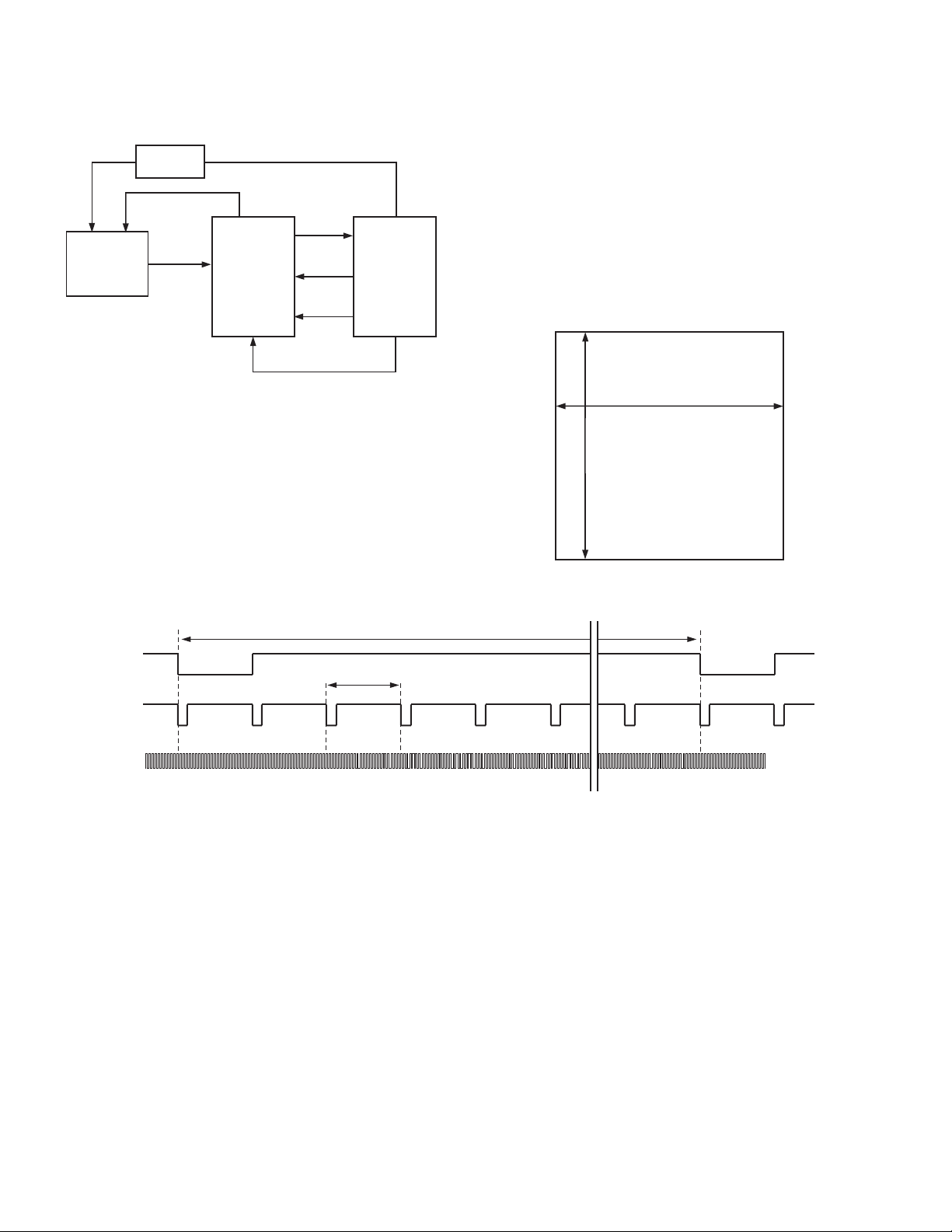
Figure 1. Typical Application
Figure 1 shows the typical system application diagram for the
AD9948. The CCD output is processed by the AD9948’s AFE
circuitry, which consists of a CDS, a PxGA, a VGA, a black level
clamp, and an A/D converter. The digitized pixel information is
sent to the digital image processor chip, where all postprocessing
and compression occurs. To operate the CCD, CCD timing
parameters are programmed into the AD9948 from the image
processor through the 3-wire serial interface. From the system
master clock, CLI, provided by the image processor, the AD9948
generates the high speed CCD clocks and all internal AFE clocks.
All AD9948 clocks are synchronized with VD and HD. All of
the AD9948’s horizontal pulses (CLPOB, PBLK, and HBLK)
are programmed and generated internally.
The H-drivers for H1–H4 and RG are included in the AD9948,
allowing these clocks to be connected directly to the CCD.
H-drive voltage of 3 V is supported in the AD9948.
Figure 2a shows the horizontal and vertical counter dimensions
for the AD9948. All internal horizontal clocking is programmed
using these dimensions to specify line and pixel locations.
MAXIMUM FIELD DIMENSIONS
12-BIT HORIZONTAL = 4096 PIXELS MAX
12-BIT VERTICAL = 4096 LINES MAX
Figure 2a. Vertical and Horizontal Counters
VD
HD
CLI
MAX VD LENGTH IS 4095 LINES
MAX HD LENGTH IS 4095 PIXELS
Figure 2b. Maximum VD/HD Dimensions
REV. 0–8–
AD9948
SERIAL INTERFACE TIMING
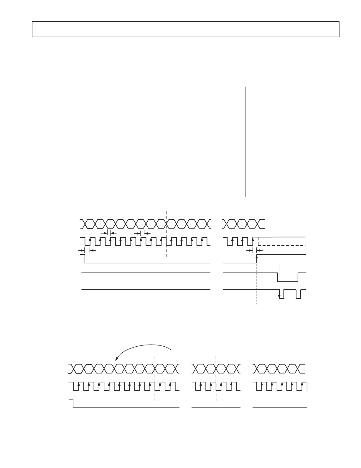
All of the internal registers of the AD9948 are accessed through
a 3-wire serial interface. Each register consists of an 8-bit address
and a 24-bit data-word. Both the 8-bit address and 24-bit dataword are written starting with the LSB. To write to each register,
a 32-bit operation is required, as shown in Figure 3a. Although
many registers are less than 24 bits wide, all 24 bits must be
written for each register. If the register is only 16 bits wide, then
the upper eight bits are don’t cares and may be filled with zeros
during the serial write operation. If fewer than 24 bits are written,
the register will not be updated with new data.
Figure 3b shows a more efficient way to write to the registers by
using the AD9948’s address auto-increment capability. Using
this method, the lowest desired address is written first, followed
by multiple 24-bit data-words. Each new 24-bit data-word will
be written automatically to the next highest register address. By
eliminating the need to write each 8-bit address, faster register
loading is achieved. Address auto-increment may be used starting with any register location, and may be used to write to as
few as two registers or as many as the entire register space.
8-BIT ADDRESS
COMPLETE REGISTER LISTING
All addresses and default values are expressed in hexadecimal.
All registers are VD/HD updated as shown in Figure 3a, except
for the registers indicated in Table I, which are SL updated.
Table I. SL-Updated Registers
Register Description
OPRMODE AFE Operation Modes
CTLMODE AFE Control Modes
SW_RESET Software Reset Bit
TGCORE _RSTB Reset Bar Signal for Internal TG Core
PREVENTUPDATE Prevents Update of Registers
VDHDEDGE VD/HD Active Edge
FIELDVAL Resets Internal Field Pulse
HBLKRETIME Retimes the HBLK to Internal Clock
CLPBLKOUT CLP/BLK Output Pin Select
CLPBLKEN Enables CLP/BLK Output Pin
H1CONTROL H1/H2 Polarity Control
RGCONTROL H1 Positive Edge Location
DRVCONTROL H1 Negative Edge Location
SAMPCONTROL H1 Drive Current
DOUTPHASE H2 Drive Current
24-BIT DATA
SDATA
SCK
SDATA
SCK
A0 A1 A2 A4 A5 A6 A7
t
DS
1 32234567891011 12 30 31
t
LS
SL
VD
HD
NOTES
1. INDIVIDUAL SDATA BITS ARE LATCHED ON SCK RISING EDGES.
2. ALL 32 BITS MUST BE WRITTEN: 8 BITS FOR ADDRESS AND 24 BITS FOR DATA.
3. IF THE REGISTER LENGTH IS <24 BITS, THEN DON’T CARE BITS MUST BE USED TO COMPLETE THE 24-BIT DATA LENGTH.
4. NEW DATA IS UPDATED AT EITHER THE SL RISING EDGE OR AT THE HD FALLING EDGE AFTER THE NEXT VD FALLING EDGE.
5. VD/HD UPDATE POSITION MAY BE DELAYED TO ANY HD FALLING EDGE IN THE FIELD USING THE UPDATE REGISTER.
A3
t
DH
D1 D2 D3 D21 D22 D23
D0
...
...
...
...
...
t
LH
SL UPDATED
Figure 3a. Serial Write Operation
DATA FOR STARTING
REGISTER ADDRESS
A0 A1 A2 A4 A5 A6 A7 D0 D1 D22 D23
1 322345678910 31
A3
...
...
DATA FOR NEXT
REGISTER ADDRESS
D0 D1 D22 D23
...
...
3433 5655
VD/HD UPDATED
D0
D2D1
585759
...
...
REV. 0
SL
NOTES
1. MULTIPLE SEQUENTIAL REGISTERS MAY BE LOADED CONTINUOUSLY.
2. THE FIRST (LOWEST ADDRESS) REGISTER ADDRESS IS WRITTEN, FOLLOWED BY MULTIPLE 24-BIT DATA-WORDS.
3. THE ADDRESS WILL AUTOMATICALLY INCREMENT WITH EACH 24-BIT DATA-WORD (ALL 24 BITS MUST BE WRITTEN).
4. SL IS HELD LOW UNTIL THE LAST DESIRED REGISTER HAS BEEN LOADED.
5. NEW DATA IS UPDATED AT EITHER THE SL RISING EDGE OR AT THE HD FALLING EDGE AFTER THE NEXT VD FALLING EDGE.
...
...
Figure 3b. Continuous Serial Write Operation
–9–
...
 Loading...