Complete 12-Bit 40 MHz
CCD Signal Processor
AD9945
FEATURES
40 MSPS Correlated Double Sampler (CDS)
6 dB to 40 dB 10-Bit Variable Gain Amplifier (VGA)
Low Noise Optical Black Clamp Circuit
Preblanking Function
12-Bit 40 MSPS A/D Converter
No Missing Codes Guaranteed
3-Wire Serial Digital Interface
3 V Single-Supply Operation
Low Power: 140 mW @ 3 V Supply
Space-Saving 32-Lead 5 mm
5 mm LFCSP
APPLICATIONS
Digital Still Cameras
Digital Video Camcorders
PC Cameras
Portable CCD Imaging Devices
CCTV Cameras
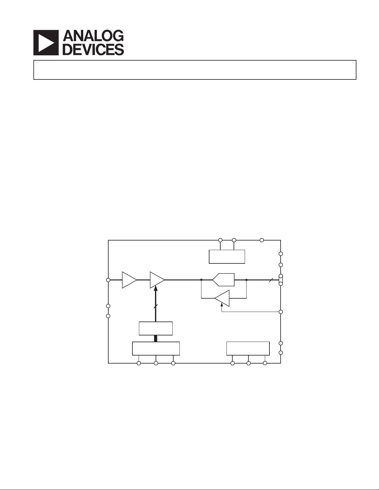
FUNCTIONAL BLOCK DIAGRAM
AD9945
6dB TO 40dB
CCDIN
VGACDS
GENERAL DESCRIPTION
The AD9945 is a complete analog signal processor for CCD
applications. It features a 40 MHz single-channel architecture
designed to sample and condition the outputs of interlaced and
progressive scan area CCD arrays. The AD9945’s signal chain
consists of a correlated double sampler (CDS), a digitally controlled variable gain amplifier (VGA), a black level clamp, and a
12-bit A/D converter.
The internal registers are programmed through a 3-wire serial digital
interface. Programmable features include gain adjustment, black
level adjustment, input clock polarity, and power-down modes.
The AD9945 operates from a single 3 V power supply, typically dissipates 140 mW, and is packaged in a space-saving
32-lead LFCSP.
REFT
REFB
BAND GAP
REFERENCE
12-BIT
ADC
PBLK
DRVDD
DRVSS
12
DOUT
SL
10
CONTROL
REGISTERS
DIGITAL
INTERFACE
SDATASCK
AVDD
AVSS
REV. A
Information furnished by Analog Devices is believed to be accurate and
reliable. However, no responsibility is assumed by Analog Devices for its
use, nor for any infringements of patents or other rights of third parties that
may result from its use. No license is granted by implication or otherwise
under any patent or patent rights of Analog Devices. Trademarks and
registered trademarks are the property of their respective owners.
CLP
CLPOB
INTERNAL
TIMING
DATACLKSHDSHP
One Technology Way, P.O. Box 9106, Norwood, MA 02062-9106, U.S.A.
Tel: 781/329-4700 www.analog.com
Fax: 781/326-8703 © 2003 Analog Devices, Inc. All rights reserved.
DVDD
DVSS

AD9945–SPECIFICATIONS
(T
to T
GENERAL SPECIFICATIONS
MIN
, AVDD = DVDD = DRVDD= 3.0 V, f
MAX
Parameter Min Typ Max Unit
TEMPERATURE RANGE
Operating –20 +85 °C
Storage –65 +150 °C
POWER SUPPLY VOLTAGE
Analog, Digital, Digital Driver 2.7 3.6 V
POWER CONSUMPTION
Normal Operation (DRVDD Power not Included) 140 mW
DRVDD Power Only (C
= 20 pF) 10 mW
LOAD
Power-Down Mode 1.5 mW
MAXIMUM CLOCK RATE 40 MHz
Specifications subject to change without notice.
= 40 MHz, unless otherwise noted.)
SAMP
DIGITAL SPECIFICATIONS
(DRVDD = DVDD = 2.7 V, CL = 20 pF, unless otherwise noted.)
Parameter Symbol Min Typ Max Unit
LOGIC INPUTS
High Level Input Voltage V
Low Level Input Voltage V
High Level Input Current I
Low Level Input Current I
Input Capacitance C
IH
IL
IH
IL
IN
2.1 V
0.6 V
10 µA
10 µA
10 pF
LOGIC OUTPUTS
High Level Output Voltage, I
Low Level Output Voltage, IOL = 2 mA V
Specifications subject to change without notice.
= 2 mA V
OH
OH
OL
2.2 V
0.5 V
REV. A–2–

AD9945
SYSTEM SPECIFICATIONS
(T
to T
MIN
, AVDD = DVDD = DRVDD = 3.0 V, f
MAX
= 40 MHz, unless otherwise noted.)
SAMP
Parameter Min Typ Max Unit Notes
CDS
Maximum Input Range before Saturation* 1.0 Vp-p
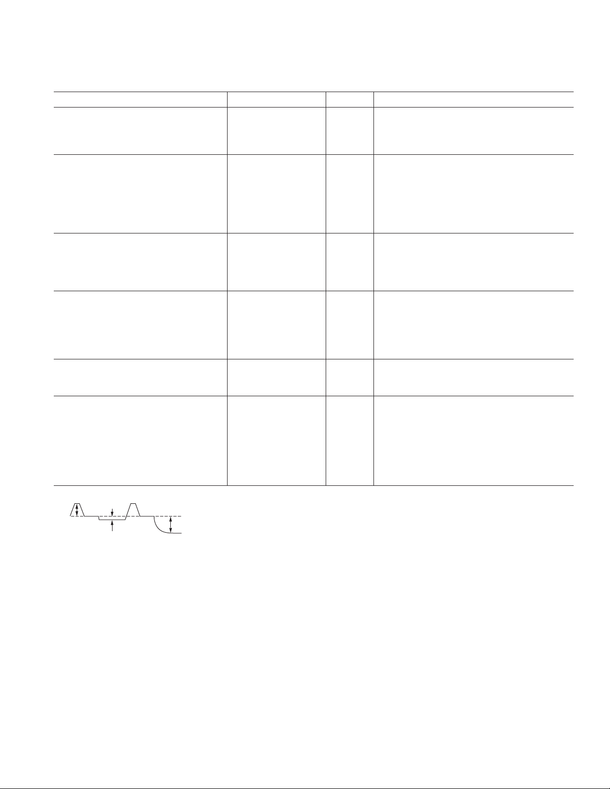
Allowable CCD Reset Transient* 500 mV See Input Waveform in Footnote
Maximum CCD Black Pixel Amplitude* 100 mV
VARIABLE GAIN AMPLIFIER (VGA)
Gain Control Resolution 1024 Steps
Gain Monotonicity Guaranteed
Gain Range
Minimum Gain 5.3 dB See Figure 7 for VGA Gain Curve
Maximum Gain 40.0 41.5 dB See Variable Gain Amplifier Section for
VGA Gain Equation
BLACK LEVEL CLAMP
Clamp Level Resolution 256 Steps
Clamp Level Measured at ADC Output
Minimum Clamp Level 0 LSB
Maximum Clamp Level 255 LSB
A/D CONVERTER
Resolution 12 Bits
Differential Nonlinearity (DNL) ± 0.5 LSB
No Missing Codes Guaranteed
Data Output Coding Straight Binary
Full-Scale Input Voltage 2.0 V
VOLTAGE REFERENCE
Reference Top Voltage (REFT) 2.0 V
Reference Bottom Voltage (REFB) 1.0 V
SYSTEM PERFORMANCE Specifications Include Entire Signal Chain
Gain Range
Low Gain (VGA Code = 0) 5.3 dB
Maximum Gain (VGA Code = 1023) 40.0 41.5 dB
Gain Accuracy 1.0 dB
Peak Nonlinearity, 500 mV Input Signal 0.1 % 12 dB Gain Applied
Total Output Noise 1.2 LSB rms AC Grounded Input, 6 dB Gain Applied
Power Supply Rejection (PSR) 40 dB
*Input Signal Characteristics defined as follows:
500mV TYP
RESET TRANSIENT
Specifications subject to change without notice.
100mV TYP
OPTICAL BLACK PIXEL
1V TYP
INPUT SIGNAL RANGE
REV. A
–3–

AD9945
TIMING SPECIFICATIONS
(CL = 20 pF, f
= 40 MHz, CCD Mode Timing in Figures 8 and 9, Serial Timing in Figures 4 and 5.)
SAMP
Parameter Symbol Min Typ Max Unit
SAMPLE CLOCKS
DATACLK, SHP, SHD Clock Period t
DATACLK High/Low Pulse Width t
SHP Pulse Width t
SHD Pulse Width t
CLPOB Pulse Width* t
SHP Rising Edge to SHD Falling Edge t
SHP Rising Edge to SHD Rising Edge t
Internal Clock Delay t
CONV
ADC
SHP
SHD
COB
S1
S2
ID
25 ns
10 12.5 ns
6.25 ns
6.25 ns
220 Pixels
6.25 ns
11.25 12.5 ns
3ns
DATA OUTPUTS
Output Delay t
OD
9.5 ns
Pipeline Delay 10 Cycles
SERIAL INTERFACE
Maximum SCK Frequency f
SL to SCK Setup Time t
SCK to SL Hold Time t
SDATA Valid to SCK Rising Edge Setup t
SCK Falling Edge to SDATA Valid Hold t
*Minimum CLPOB pulse width is for functional operation only. Wider typical pulses are recommended to achieve low noise clamp performance.
Specifications subject to change without notice.
SCLK
LS
LH
DS
DH
10 MHz
10 ns
10 ns
10 ns
10 ns
ABSOLUTE MAXIMUM RATINGS*
With
Respect
Parameter To Min Max Unit
AVDD AVSS –0.3 +3.9 V
DVDD DVSS –0.3 +3.9 V
DRVDD DRVSS –0.3 +3.9 V
Digital Outputs DRVSS –0.3 DRVDD + 0.3 V
SHP, SHD, DATACLK DVSS –0.3 DVDD + 0.3 V
CLPOB, PBLK DVSS –0.3 DVDD + 0.3 V
SCK, SL, SDATA DVSS –0.3 DVDD + 0.3 V
REFT, REFB, CCDIN AVSS –0.3 AVDD + 0.3 V
Junction Temperature 150 °C
Lead Temperature 300 °C
(10 sec)
*Stresses above those listed under Absolute Maximum Ratings may cause perma-
nent damage to the device. This is a stress rating only; functional operation of the
device at these or any other conditions outside of those indicated in the operational
sections of this specification is not implied. Exposure to absolute maximum ratings
for extended periods may affect device reliability.
ORDERING GUIDE
Temperature Package Package
Model Range Description1Option
AD9945KCP –20°C to +85°C LFCSP CP-32
AD9945KCPRL –20°C to +85°C LFCSP CP-32
AD9945KCPRL7 –20°C to +85°C LFCSP CP-32
AD9945KCPZ
2
–20°C to +85°C LFCSP CP-32
AD9945KCPZRL72–20°C to +85°C LFCSP CP-32
1
LFCSP = Lead Frame Chip Scale Package
2
Z = Pb-free part.
THERMAL CHARACTERISTICS
Thermal Resistance
32-Lead LFCSP Package
= 27.7 °C/W
θ
JA
CAUTION
ESD (electrostatic discharge) sensitive device. Electrostatic charges as high as 4000 V readily
accumulate on the human body and test equipment and can discharge without detection. Although the
AD9945 features proprietary ESD protection circuitry, permanent damage may occur on devices
subjected to high energy electrostatic discharges. Therefore, proper ESD precautions are recommended
to avoid performance degradation or loss of functionality.
REV. A–4–

PIN CONFIGURATION
32 D1
31 D0
30 NC
29 NC
28 NC
27 SCK
26 SDATA
25 SL
AD9945
D2 1
D3 2
D4 3
D5 4
D6 5
D7 6
D8 7
D9 8
PIN 1
INDICATOR
AD9945
TOP VIEW
D11 10
D10 9
DRVDD 11
DVDD 13
DRVSS 12
DVSS 15
DATACLK 14
PBLK 16
24 REFB
23 REFT
22 CCDIN
21 AVSS
20 AVDD
19 SHD
18 SHP
17 CLPOB
PIN FUNCTION DESCRIPTIONS
Pin Number Mnemonic Type Description
1 to 10, 31, 32 D2 to D11, D0, D1 DO Digital Data Outputs
11 DRVDD P Digital Output Driver Supply
12 DRVSS P Digital Output Driver Ground
13 DVDD P Digital Supply
14 DATACLK DI Digital Data Output Latch Clock
15 DVSS P Digital Supply Ground
16 PBLK DI Preblanking Clock Input
17 CLPOB DI Black Level Clamp Clock Input
18 SHP DI CDS Sampling Clock for CCD’s Reference Level
19 SHD DI CDS Sampling Clock for CCD’s Data Level
20 AVDD P Analog Supply
21 AVSS P Analog Ground
22 CCDIN AI Analog Input for CCD Signal
23 REFT AO A/D Converter Top Reference Voltage Decoupling
24 REFB AO A/D Converter Bottom Reference Voltage Decoupling
25 SL DI Serial Digital Interface Load Pulse
26 SDATA DI Serial Digital Interface Data Input
27 SCK DI Serial Digital Interface Clock Input
28 to 30 NC NC Internally Pulled Down. Float or connect to GND.
TYPE: AI = Analog Input, AO = Analog Output, DI = Digital Input, DO = Digital Output, P = Power.
REV. A
–5–
 Loading...