A
Dual-Channel, 14-Bit, CCD Signal Processor
FEATURES OF EACH CHANNEL
40 MHz correlated double sampler (CDS)
0 dB to 18 dB, 9-bit variable gain amplifier (VGA)
40 MSPS analog-to-digital converter (ADC)
Black level clamp with variable level control
Complete on-chip timing driver
Precision Timing Core with <550 ps resolution
On-chip 3 V horizontal and RG drivers
4-phase H-clock mode
100-lead, 9 mm × 9 mm, CSP_BGA package
APPLICATIONS
Signal processor for dual-channel CCD outputs
Digital still cameras
Digital video cameras
High speed digital imaging applications
with
Precision Timing
™ Core
AD9942
GENERAL DESCRIPTION
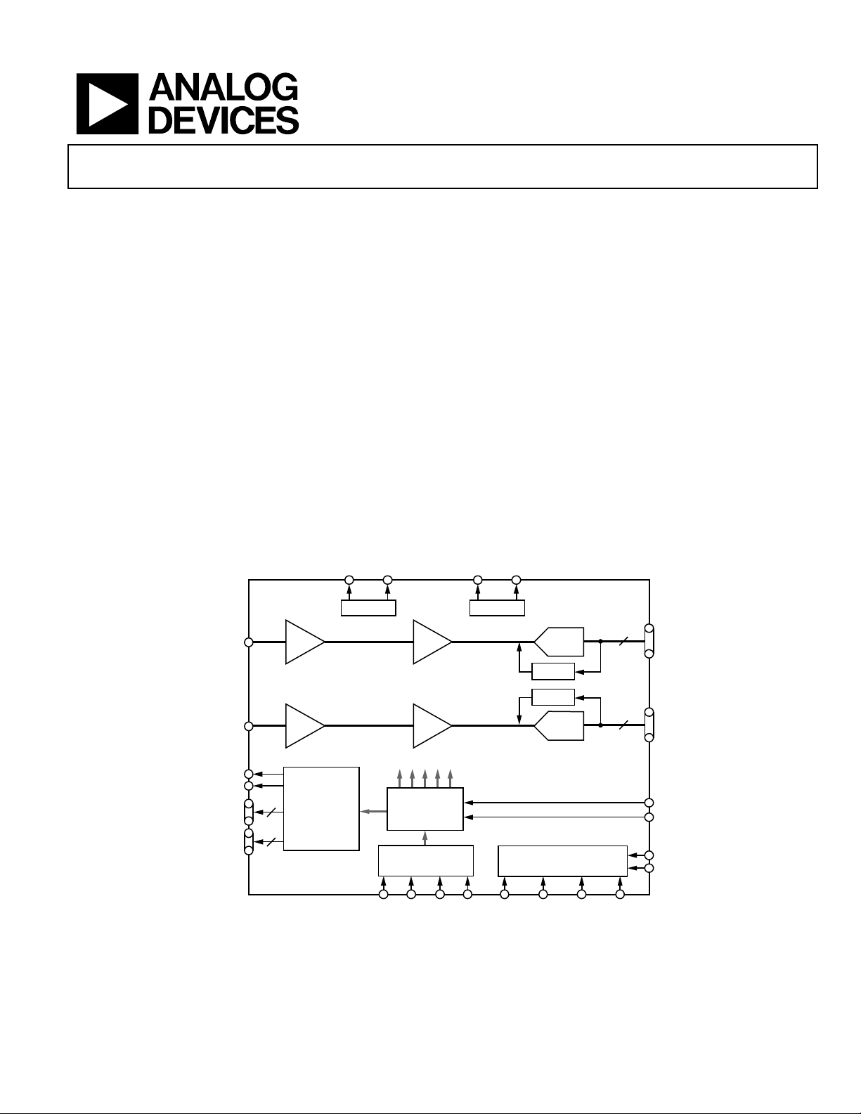
The AD9942 is a highly integrated dual-channel CCD signal
processor for digital still camera applications. Each channel is
specified at pixel rates of up to 40 MHz. The AD9942 consists of
a complete analog front end with analog-to-digital conversion,
combined with a programmable timing driver. The Precision
Timi ng Core allows high speed clocks to be adjusted with
550 ps resolution.
The analog front end uses black level clamping and includes a
VGA, a 40 MSPS ADC, and a CDS. The timing driver provides
the high speed CCD clock drivers for RG_A, RG_B, and the
H1A to H4A and H1B to H4B outputs. The 6-wire serial
interface is used to program the AD9942.
Available in a space-saving, 9 mm × 9 mm, CSP_BGA package,
the AD9942 is specified over an operating temperature range of
−25°C to +85°C.
CCDIN_A
CCDIN_B
RG_A
RG_B
H1A TO H4
H1B TO H4B
AD9942
4
4
CDS
CDS
HORIZONTAL
DRIVERS
FUNCTIONAL BLOCK DIAGRAM
0dB
0dB
Figure 1.
REFT_B REFB_B
VREF_B
~
18dB
~
18dB
SL_A
SDATA_A
REFT_A REFB_A
VREF_A
INTERNAL CLOCKS
HD_A VD_A HD_B VD_B
VGA
VGA
PRECISION
TIMING
CORE
SYNC
GENERATOR
ADC
CLAMP
CLAMP
ADC
INTERNAL
REGISTERS
SL_B
14
14
SDATA_B
DOUT_A
DOUT_B
CLI_A
CLI_B
SCK_A
SCK_B
05240-001
Rev. 0
Information furnished by Analog Devices is believed to be accurate and reliable.
However, no responsibility is assumed by Analog Devices for its use, nor for any
infringements of patents or other rights of third parties that may result from its use.
Specifications subject to change without notice. No license is granted by implication
or otherwise under any patent or patent rights of Analog Devices. Trademarks and
registered trademarks are the property of their respective owners.
One Technology Way, P.O. Box 9106, Norwood, MA 02062-9106, U.S.A.
Tel: 781.329.4700
Fax: 781.326.8703 © 2005 Analog Devices, Inc. All rights reserved.
www.analog.com

AD9942
TABLE OF CONTENTS
General Specifications...................................................................... 3
Digital Specifications........................................................................ 4
Channel A and Channel B Horizontal Clamping
and Blanking ................................................................................... 22
Individual CLPOB and PBLK Sequences................................ 22
Analog Specifications....................................................................... 5
Channel-to-Channel Specifications ............................................... 6
Timing Specifications....................................................................... 7
Absolute Maximum Ratings............................................................ 8
Thermal Resistance ...................................................................... 8
ESD Caution.................................................................................. 8
Pin Configuration and Function Descriptions............................. 9
Te r mi n ol o g y .................................................................................... 11
Equivalent Input/Output Circuits................................................ 12
Typical Performance Characteristics ........................................... 13
System Overview ............................................................................ 14
Serial Interface Timing .................................................................. 15
Complete Register Listing......................................................... 16
Channel A and Channel B Precision Timing............................... 19
High Speed Timing Generation ............................................... 19
Timing Resolution...................................................................... 19
High Speed Clock Programmability ........................................ 19
H-Driver and RG Outputs ........................................................21
Digital Data Outputs.................................................................. 21
Individual HBLK Sequences..................................................... 22
Channel A and Channel B Special HBLK Patterns.................... 24
Horizontal Sequence Control ................................................... 24
H-Counter Synchronization..................................................... 24
Channel A and Channel B Power-Up Procedure....................... 25
Channel A and Channel B Analog Front End Operation......... 26
DC Restore .................................................................................. 26
Correlated Double Sampler ...................................................... 26
Channel A and Channel B Variable Gain Amplifier............. 27
Channel A and Channel B ADC .............................................. 27
Channel A and Channel B Optical Black Clamp ................... 27
Channel A and Channel B Digital Data Outputs................... 27
Applications Information.............................................................. 28
Circuit Configuration ................................................................ 28
Grounding/Decoupling Recommendations ........................... 28
Driving the CLI Input................................................................ 30
Horizontal Timing Sequence Example.................................... 30
Outline Dimensions ....................................................................... 32
Ordering Guide .......................................................................... 32
REVISION HISTORY
1/05—Revision 0: Initial Version
Rev. 0 | Page 2 of 32

AD9942
GENERAL SPECIFICATIONS
In Table 1, X = A, B.
Table 1.
Parameter Min Typ Max Unit
TEMPERATURE RANGE
Operating
Storage
−25
−65
MAXIMUM CLOCK RATE 40 MHz
POWER SUPPLY VOLTAGE
AVDD_X, TCVDD_X (AFE, Timing Core) 2.7 3.0 3.6 V
HVDD_X (H1X to H4X Drivers) 2.7 3.0 3.6 V
RGVDD_X (RG_X Driver) 2.7 3.0 3.6 V
DRVDD_X (D0 to D13 Drivers) 2.7 3.0 3.6 V
DVDD_X (Digital) 2.7 3.0 3.6 V
POWER DISSIPATION FOR EACH CHANNEL
(40 MHz, 3 V Supplies, 100 pF H1X to H4X Loading, 10 pF RG_X Loading)
Power from AVDD_X 110 mW
Power from TCVDD_X 33 mW
Power from HVDD_X
1
160 mW
Power from RGVDD_X 13 mW
Power from DRVDD_X 15 mW
Power from DVDD_X 40 mW
Total Shutdown Mode 2 mW
1
Total HVDD_X Power = [(C
) × (HVDD_X) × (Pixel Frequency)] × (HVDD_X) × (Number of Horizontal Outputs Used).
LOAD
+85 °C
+150 °C
Rev. 0 | Page 3 of 32

AD9942
DIGITAL SPECIFICATIONS
T
to T
MIN
In Table 2, X = A, B.
Table 2.
Parameter Symbol Min Typ Max Unit
LOGIC INPUTS
High Level Input Voltage V
Low Level Input Voltage V
High Level Input Current I
Low Level Input Current I
Input Capacitance CIN 10 pF
LOGIC OUTPUTS
High Level Output Voltage, IOH = 2 mA V
Low Level Output Voltage, IOL = 2 mA VOL 0.5 V
CLI INPUT
High Level Input Voltage (TCVDD_X/2 + 0.5 V) V
Low Level Input Voltage V
RG_X AND H1X TO H4X DRIVER OUTPUTS
High Level Output Voltage (RGVDD_X – 0.5 V and HVDD_X – 0.5 V) VOH 2.2 V
Low Level Output Voltage V
Maximum Output Current (Programmable) 30 mA
Maximum Load Capacitance 100 pF
, AVDD_X = DVDD_X = DRVDD_X = HVDD_X = RGVDD_X = 2.7 V, CL = 20 pF, unless otherwise noted.
MAX
IH
IL
IH
IL
OH
IH – CLI
IL – CLI
OL
2.1 V
0.6 V
10 µA
10 µA
2.2 V
1.85 V
0.85 V
0.5 V
Rev. 0 | Page 4 of 32

AD9942
ANALOG SPECIFICATIONS
T
to T
MIN
Table 3.
Parameter Min Typ Max Unit Notes
CDS
Gain 0 dB
Allowable CCD Reset Transient
Max Input Range before Saturation 1.0 V p-p
Max CCD Black Pixel Amplitude ±100 mV Measured at 12 dB VGA gain
VARIABLE GAIN AMPLIFIER (VGA_X)
Max Input Range 1.0 V p-p
Max Output Range 2.0 V p-p
Gain Control Resolution 512 Steps
Gain Monotonicity Guaranteed
Gain Range
BLACK LEVEL CLAMP
Clamp Level Resolution 256 Steps 4 LSB/step
Clamp Level Measured at ADC output
CHN_A AND CHN_B ADC
Differential Nonlinearity (DNL) −1.0 ± 0.5 +1.0 LSB
No Missing Codes Guaranteed
Full-Scale Input Voltage 2.0 V
VOLTAGE REFERENCE
Reference Top Voltage (REFT_X) 2.0 V
Reference Bottom Voltage (REFB_X) 1.0 V
SYSTEM PERFORMANCE Specifications include entire signal chain
VGA Gain Accuracy
Peak Nonlinearity, 500 mV Input Signal 0.15 % 12 dB gain applied
Total Output Noise 3 LSB rms AC grounded input, 6 dB gain applied
Power Supply Rejection (PSR) 50 dB Measured with step change on supply
1
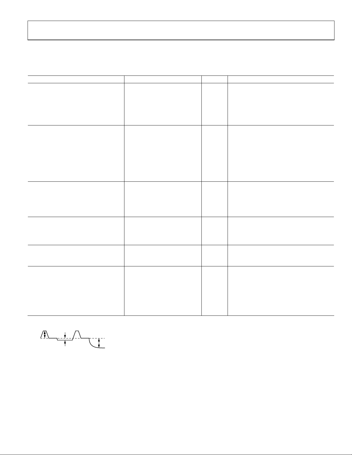
Input signal characteristics defined as follows:
, AVDD_X = DVDD_X = 3.0 V, f
MAX
1
= 40 MHz, typical timing specifications, unless otherwise noted. In Table 3, X = A, B.
CLI
500 mV
Min Gain (Code 0) 0 dB
Max Gain (Code 511) 18 dB
Min Clamp Level 0 LSB
Max Clamp Level 1023 LSB
Min Gain (Code 0) 5 5.5 6 dB
Max Gain (Code 511) 17.5 18 18.5 dB
(Typ = 70 mV at 15 dB and 50 mV at 18 dB)
500mV TYP
RESET TRANSIENT
OPTICAL BLACK PIXEL
100mV MAX
1V MAX
INPUT SIGNAL RANGE
05240-099
Rev. 0 | Page 5 of 32

AD9942
CHANNEL-TO-CHANNEL SPECIFICATIONS
T
to T
MIN
Table 4.
Parameter Min Typ Max Unit Notes
CHANNEL A/CHANNEL B OUTPUT
CODE MATCHING ERROR
CROSSTALK ERROR VGA = 6 dB, 12 dB, and 18 dB conditions.
Channel A to Channel B
Channel B to ChannelA
1
Matching error calculated using a ramp input applied to Channel A and Channel B simultaneously. Typical Channel A/Channel B error is < 1.0% at each output code.
, AVDD_X = DVDD_X = 3.0 V, f
MAX
1
= 40 MHz, typical timing specifications, unless otherwise noted. In Table 4, X = A, B.
CLI
< 1.0 % VGA = 6 dB, 12 dB, and 18 dB conditions.
−84
dB
Full-scale step applied to Channel A while
measuring response on Channel B.
−84
dB
Full-scale step applied to Channel B while
measuring response on Channel A.
Rev. 0 | Page 6 of 32

AD9942
TIMING SPECIFICATIONS
CL = 20 pF, f
Table 5.
Parameter Symbol Min Typ Max Unit
MASTER CLOCK (CLI_X) (See Figure 16)
CLI_X Clock Period 25.0 ns
CLI_X High/Low Pulse Width t
Delay from CLI_X to Internal Pixel
Period Position (See Figure 16) t
CLPOB_X PULSE WIDTH (Programmable)
SAMPLE CLOCKS (See Figure 18)
SHP_X Rising Edge to SHD_X Rising Edge t
DATA OUTPUTS (See Figure 19 and Figure 20)
Output Delay from Programmed Edge t
Pipeline Delay 11 Cycles
SERIAL INTERFACE
Maximum SCK_X Frequency f
SL_X to SCK_X Setup Time t
SCK to SL_X Hold Time t
SDATA_X Valid to SCK_X Rising Edge Setup t
SCK_X Falling Edge to SDATA_X Valid Hold t
SCK_X Falling Edge to SDATA_X Valid Read t
1
Minimum CLPOB pulse width is for functional operation only. Wider typical pulses are recommended to achieve low noise clamp reference.
= 40 MHz, serial timing in Figure 14 and Figure 15, unless otherwise noted. In Table 5, X = A, B.
CLI
ADC
1
CLIDLY
t
2 20 Pixels
COB
S1
OD
SCLK
LS
LH
DS
DH
DV
10.0 12.5 15.0 ns
6 ns
11.2 12.5 ns
6 ns
10 MHz
10 ns
10 ns
10 ns
10 ns
10 ns
Rev. 0 | Page 7 of 32

AD9942
ABSOLUTE MAXIMUM RATINGS
Table 6. Ratings (X = A, B)
Parameter Rating
AVDD_X and TCVDD_X to AVSS_X −0.3 V to +3.9 V
HVDD_X and RGVDD_X to
HVSS_X and RGVSS_X
DVDD_X and DRVDD_X to
DVSS_X and DRVSS_X
Any VSS_X to Any VSS_X −0.3 V to +0.3 V
Digital Outputs to DRVSS_X −0.3 V to DRVDD + 0.3 V
SCK_X, SL_X, and SDATA_X to
DVSS_X
RG_X to RGVSS_X −0.3 V to RGVDD + 0.3 V
H1X to H4X to HVSS_X −0.3 V to HVDD + 0.3 V
REFT_X, REFB_X, and CCDIN_X to
AVSS_X
Junction Temperature 150°C
Lead Temperature (10 sec) 300°C
−0.3 V to +3.9 V
−0.3 V to +3.9 V
−0.3 V to DVDD + 0.3 V
−0.3 V to AVDD + 0.3 V
Stresses above those listed under Absolute Maximum Ratings
may cause permanent damage to the device. This is a stress
rating only; functional operation of the device at these or any
other conditions above those listed in the operational sections
of this specification is not implied. Exposure to absolute
maximum rating conditions for extended periods may affect
device reliability.
THERMAL RESISTANCE
100-lead, 9 mm × 9 mm, CSP_BGA package: θJA = 38.3°C/W
1
θJA is measured using a 4-layer PCB with the exposed paddle soldered to the
board.
1
ESD CAUTION
ESD (electrostatic discharge) sensitive device. Electrostatic charges as high as 4000 V readily accumulate on
the human body and test equipment and can discharge without detection. Although this product features
proprietary ESD protection circuitry, permanent damage may occur on devices subjected to high energy
electrostatic discharges. Therefore, proper ESD precautions are recommended to avoid performance
degradation or loss of functionality.
Rev. 0 | Page 8 of 32

AD9942
PIN CONFIGURATION AND FUNCTION DESCRIPTIONS
A1 CORNER
INDEX AREA
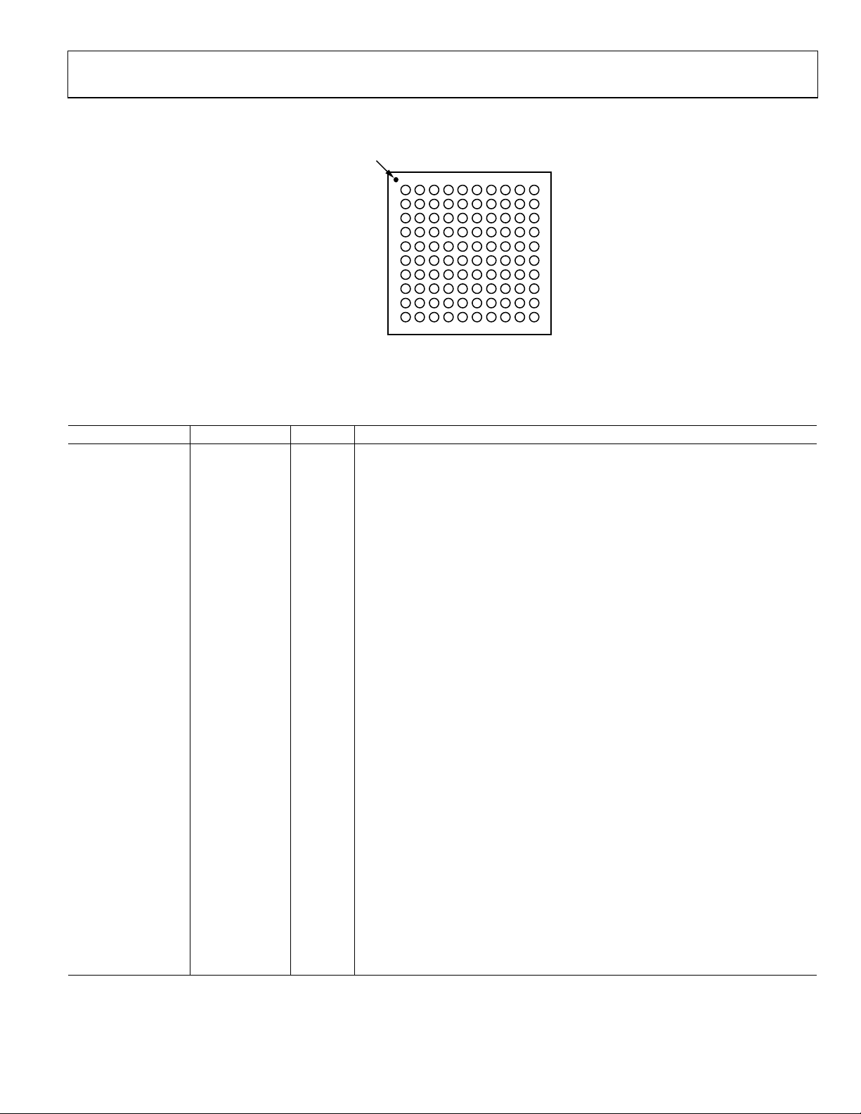
Table 7. Pin Function Descriptions
Ball Location Mnemonic Type1 Description
B2 SL_A DI 6-Wire Serial Load for Channel A
C2 SDATA_A DI 6-Wire Serial Data for Channel A
D2 SCK_A DI 6-Wire Serial Clock for Channel A
C1 REFT_A AO Reference Top Decoupling for Channel A (decouple with 1.0 µF to AVSS_A)
D1 REFB_A AO Reference Bottom Decoupling for Channel A (decouple with 1.0 µF to AVSS_A)
A1 CCDIN_A AI Analog Input for Channel A CCD Signal (connect through Series 0.1 µF capacitor)
F4 H1A DO CCD Horizontal Clock 1 for Channel A
F3 H2A DO CCD Horizontal Clock 2 for Channel A
D4 H3A DO CCD Horizontal Clock 3 for Channel A
D3 H4A DO CCD Horizontal Clock 4 for Channel A
B4 RG_A DO CCD Reset Gate Clock for Channel A
J2 DRVSS_A P Digital Driver Ground for Channel A
K3 DRVDD_A P Digital Driver Supply for Channel A
E3 HVSS_A P H1A to H4A Driver Ground for Channel A
E4 HVDD_A P H1A to H4A Driver Supply for Channel A
C3 RGVSS_A P RG_A Driver Ground for Channel A
C4 RGVDD_A P RG_A Driver Supply for Channel A
B3 TCVSS_A P Analog Ground for Channel A Timing Core
A4 TCVDD_A P Analog Supply for Channel A Timing Core
B1 AVSS_A P Analog Ground for Channel A
A2 AVDD_A P Analog Ground for Channel A
F2 DVSS_A P Digital Ground for Channel A
F1 DVDD_A P Digital Supply for Channel A
E2 VD_A DI Vertical Sync Pulse for Channel A
E1 HD_A DI Horizontal Sync Pulse for Channel A
B8 SL_B DI 6-Wire Serial Load for Channel B
C8 SDATA_B DI 6-Wire Serial Data for Channel B
D8 SCK_B DI 6-Wire Serial Clock for Channel B
C7 REFT_B AO Reference Top Decoupling for Channel B (decouple with 1.0 µF to AVSS_B)
D7 REFB_B AO Reference Bottom Decoupling for Channel B (decouple with 1.0 µF to AVSS_B)
A7 CCDIN_B AI Analog Input for Channel B CCD Signal (connect through series 0.1 µF capacitor)
1
Type: AI = Analog Input, AO = Analog Output, DI = Digital Input, DO = Digital Output, P = Power.
1
2345678910
A
B
C
D
E
F
G
H
J
K
AD9942
TOP VIEW
(Not to Scale)
Figure 2. Pin Configuration
05240-002
Rev. 0 | Page 9 of 32

AD9942
Ball Location Mnemonic Type1 Description
F10 H1B DO CCD Horizontal Clock 1 for Channel B
F9 H2B DO CCD Horizontal Clock 2 for Channel B
D10 H3B DO CCD Horizontal Clock 3 for Channel B
D9 H4B DO CCD Horizontal Clock 4 for Channel B
B10 RG_B DO CCD Reset Gate Clock for Channel B
J8 DRVSS_B P Digital Driver Ground for Channel B
K9 DRVDD_B P Digital Driver Supply for Channel B
E9 HVSS_B P H1B to H4B Driver Ground for Channel B
E10 HVDD_B P H1B to H4B Driver Supply for Channel B
C9 RGVSS_B P RG_B Driver Ground for Channel B
C10 RGVDD_B P RG_B Driver Supply for Channel B
B9 TCVSS_B P Analog Ground for Channel B Timing Core
A10 TCVDD_B P Analog Supply for Channel B Timing Core
B7 AVSS_B P Analog Ground for Channel B
A8 AVDD_B P Analog Ground for Channel B
F8 DVSS_B P Digital Ground for Channel B
F7 DVDD_B P Digital Supply for Channel B
E8 VD_B DI Vertical Sync Pulse for Channel B
E7 HD_B DI Horizontal Sync Pulse for Channel B
A3 CLI_A DI Master Clock Input for Channel A
G1 D0_A DO Data Outputs Channel A
H1 D1_A DO Data Outputs Channel A
J1 D2_A DO Data Outputs Channel A
K1 D3_A DO Data Outputs Channel A
G2 D4_A DO Data Outputs Channel A
H2 D5_A DO Data Outputs Channel A
K2 D6_A DO Data Outputs Channel A
G3 D7_A DO Data Outputs Channel A
H3 D8_A DO Data Outputs Channel A
J3 D9_A DO Data Outputs Channel A
K4 D10_A DO Data Outputs Channel A
J4 D11_A DO Data Outputs Channel A
H4 D12_A DO Data Outputs Channel A
G4 D13_A DO Data Outputs Channel A
A5, B5, C5, D5, E5,
F5, G5, H5, J5, K5
A9 CLI_B DI Master Clock Input for Channel B
G7 D0_B DO Data Outputs Channel B
H7 D1_B DO Data Outputs Channel B
J7 D2_B DO Data Outputs Channel B
K7 D3_B DO Data Outputs Channel B
G8 D4_B DO Data Outputs Channel B
H8 D5_B DO Data Outputs Channel B
K8 D6_B DO Data Outputs Channel B
G9 D7_B DO Data Outputs Channel B
H9 D8_B DO Data Outputs Channel B
J9 D9_B DO Data Outputs Channel B
K10 D10_B DO Data Outputs Channel B
J10 D11_B DO Data Outputs Channel B
H10 D12_B DO Data Outputs Channel B
G10 D13_B DO Data Outputs Channel B
A6, B6, C6, D6, E6,
F6, G6, H6, J6, K6
GND P Ground Connection
GND P Ground Connection
Rev. 0 | Page 10 of 32
 Loading...