Analog Devices AD9901TQ-883, AD9901TE-883, AD9901KQ, AD9901KP Datasheet

REV. B
Information furnished by Analog Devices is believed to be accurate and
reliable. However, no responsibility is assumed by Analog Devices for its
use, nor for any infringements of patents or other rights of third parties
which may result from its use. No license is granted by implication or
otherwise under any patent or patent rights of Analog Devices.
a
Ultrahigh Speed
Phase/Frequency Discriminator
AD9901
GENERAL DESCRIPTION
The AD9901 is a digital phase/frequency discriminator capable
of directly comparing phase/frequency inputs up to 200 MHz.
Processing in a high speed trench-oxide isolated process, combined with an innovative design, gives the AD9901 a linear
detection range, free of indeterminate phase detection zones
common to other digital designs.
With a single +5 V supply, the AD9901 can be configured to
operate with TTL or CMOS logic levels; it can also operate
with ECL inputs when operated with a –5.2 V supply. The
open-collector outputs allow the output swing to be matched to
post-filtering input requirements. A simple current setting resistor controls the output stage current range, permitting a reduction in power when operated at lower frequencies.
FEATURES
Phase and Frequency Detection
ECL/TTL/CMOS Compatible
Linear Transfer Function
No “Dead Zone”
MIL-STD-883 Compliant Versions Available
APPLICATIONS
Low Phase Noise Reference Loops
Fast-Tuning “Agile” IF Loops
Secure “Hopping” Communications
Coherent Radar Transmitter/Receiver Chains
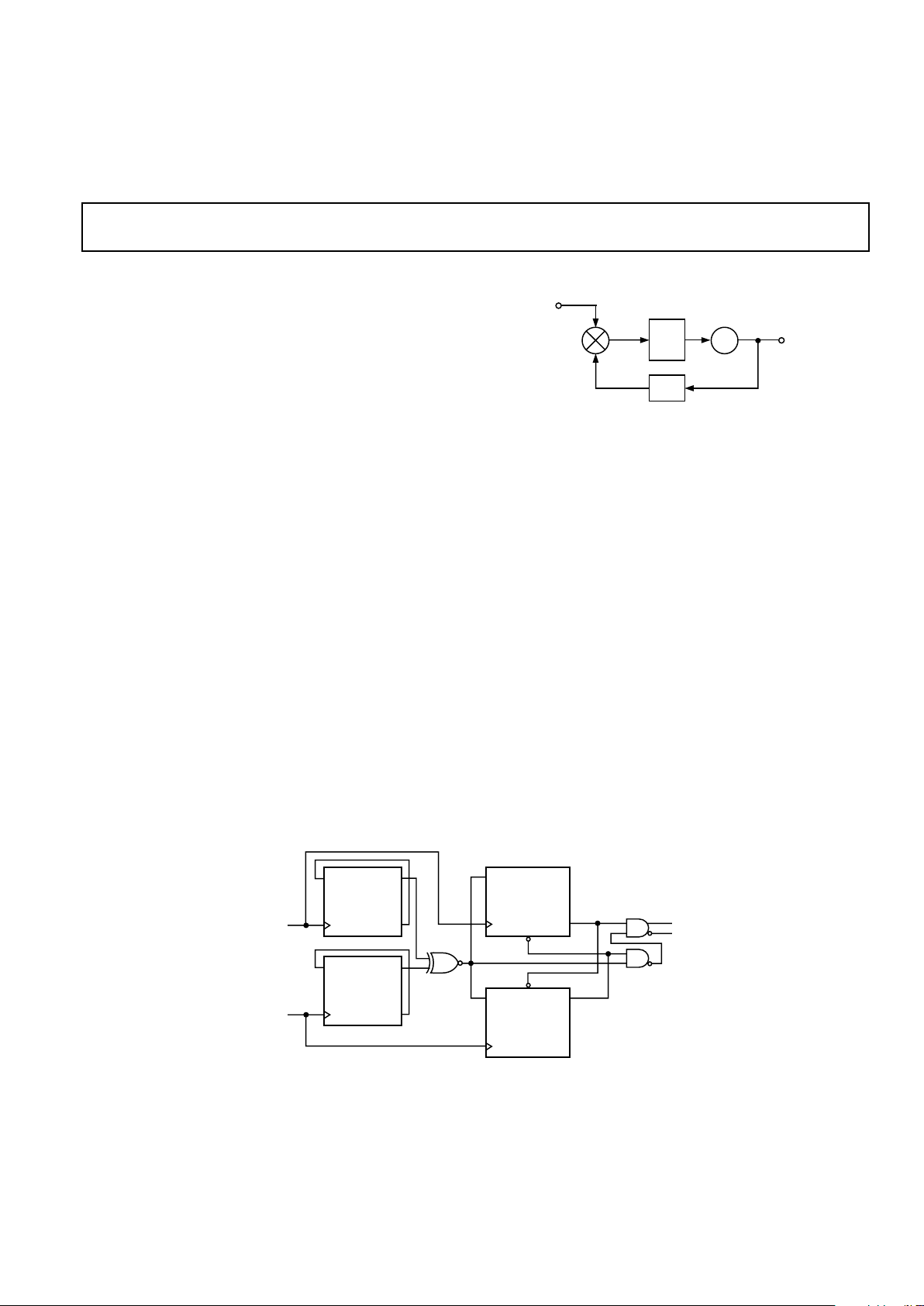
A major feature of the AD9901 is its ability to compare
phase/frequency inputs at standard IF frequencies without
prescalers. Excessive phase uncertainty which is common with
standard PLL configurations is also eliminated. The AD9901
provides the locking speed of traditional phase/frequency discriminators, with the phase stability of analog mixers.
The AD9901 is available as a commercial temperature range
device, 0°C to +70°C, and as a military temperature device,
–55°C to +125°C. The commercial versions are packaged in a
14-lead ceramic DIP and a 20-lead PLCC.
The AD9901 Phase/Frequency Discriminator is available in
versions compliant with MIL-STD-883. Refer to the Analog
Devices Military Products Databook or current AD9901/883B
data sheet for specifications.
FUNCTIONAL BLOCK DIAGRAM
OSCILLATOR
INPUT
FLIP-FLOP
DQ
Q
REFERENCE
INPUT
FLIP-FLOP
DQ
Q
XOR
OUTPUT
OUTPUT
REFERENCE
INPUT
OSCILLATOR
INPUT
OSCILLATOR
FREQUENCY
DISCRIMINATOR
FLIP-FLOP
DQ
Q
S
REFERENCE
FREQUENCY
DISCRIMINATOR
FLIP-FLOP
DQ
Q
R
PHASE-LOCKED LOOP
LOWPASS
FILTER
1/N
VCO
AD9901
REFERENCE
INPUT
OSCILLATOR
OUTPUT
OPTIONAL 1/N PRESCALER
TYPICAL OF DIGITAL PLLs
One Technology Way, P.O. Box 9106, Norwood, MA 02062-9106, U.S.A.
Tel: 781/329-4700 World Wide Web Site: http://www.analog.com
Fax: 781/326-8703 © Analog Devices, Inc., 1999

REV. B–2–
AD9901–SPECIFICATIONS
ABSOLUTE MAXIMUM RATINGS
1
Positive Supply Voltage (+VS for TTL Operation) . . . . . +7 V
Negative Supply Voltage (–V
S
for ECL Operation) . . . . . –7 V
Input Voltage Range (TTL Operation) . . . . . . . 0 V to +5.5 V
Differential Input Voltage (ECL Operation) . . . . . . . . . .4.0 V
I
SET
Current . . . . . . . . . . . . . . . . . . . . . . . . . . . . . . . . . 12 mA
Output Current . . . . . . . . . . . . . . . . . . . . . . . . . . . . . . 30 mA
ELECTRICAL CHARACTERISTICS
Commercial Temperature
0ⴗC to +70ⴗC
AD9901KQ/KP
Test
Temp Level Min Typ Max Units
INPUT CHARACTERISTICS
TTL Input Logic “1” Voltage Full VI 2.0 V
TTL Input Logic “0” Voltage Full VI 0.8 V
TTL Input Logic “1” Current
3
Full VI 0.6 mA
TTL Input Logic “0” Current
3
Full VI 1.6 mA
ECL Differential Switching Voltage Full VI 300 mV
ECL Input Current Full VI 20 µA
OUTPUT CHARACTERISTICS
Peak-to-Peak Output Voltage Swing
4
Full VI 1.6 1.8 2.0 V
TTL Output Compliance Range Full V 3–7 V
ECL Output Compliance Range Full V ±2V
I
OUT
Range Full V 0.9–11 mA
Internal Reference Voltage Full VI 0.42 0.47 0.52 V
AC CHARACTERISTICS
Linear Phase Detection Range
4
40 kHz +25°C V 360 Degrees
30 MHz +25°C V 320 Degrees
70 MHz +25°C V 270 Degrees
Functionality @ 70 MHz +25°C I Pass/Fail
POWER SUPPLY CHARACTERISTICS
TTL Supply Current (+5.0 V)
5, 6
+25°C I 43.5 54.0 mA
Full I 43.5 54.0 mA
ECL Supply Current (–5.2 V)
5, 6
+25°C I 42.5 52.5 mA
Full I 42.5 52.5 mA
Nominal Power Dissipation +25°C V 218 mW
NOTES
1
Absolute maximum ratings are limiting values, to be applied individually, and beyond which the service ability of the circuit may be impaired. Functional operability
is not necessarily implied. Exposure to absolute maximum rating conditions for an extended period of time may affect device reliability.
2
Maximum junction temperature should not exceed +175 °C for ceramic packages, +150°C for plastic packages. Junction temperature can be calculated by:
t
J
= PD (θ
JA
) +t
A
= PD (θ
JC
) +t
C
where:
PD = power dissipation
θJA = thermal impedance from junction to air (°C/W)
θJC = thermal impedance from junction to case (°C/W)
t
A
= ambient temperature (°C)
t
C
= case temperature (°C)
typical thermal impedances:
AD9901 Ceramic DIP = θJA = 74°C/W; θJC = 21°C/W
AD9901 LCC = θJA = 80°C/W; θJC = 19°C/W
AD9901 PLCC = θJA = 88.2°C/W; θJC = 45.2°C/W
3
VL = +0.4 V; VH = +2.4 V.
4
R
SET
= 47.5 Ω; RL = 182 Ω.
5
lncludes load current of 10 mA (load resistors = 182 Ω).
6
Supply should remain stable within ±5% for normal operation.
Specifications subject to change without notice.
Operating Temperature Range
AD9901KQ/KP . . . . . . . . . . . . . . . . . . . . . . . 0°C to +70°C
Storage Temperature Range . . . . . . . . . . . . –65°C to +150°C
Junction Temperature
2
Plastic . . . . . . . . . . . . . . . . . . . . . . . . . . . . . . . . . . .+150°C
Ceramic . . . . . . . . . . . . . . . . . . . . . . . . . . . . . . . . . .+175°C
Lead Soldering Temperature (10 sec) . . . . . . . . . . . . .+300°C
(ⴞVS = +5.0 V [for TTL] or –5.2 V [for ECL], unless otherwise noted)

AD9901
REV. B –3–
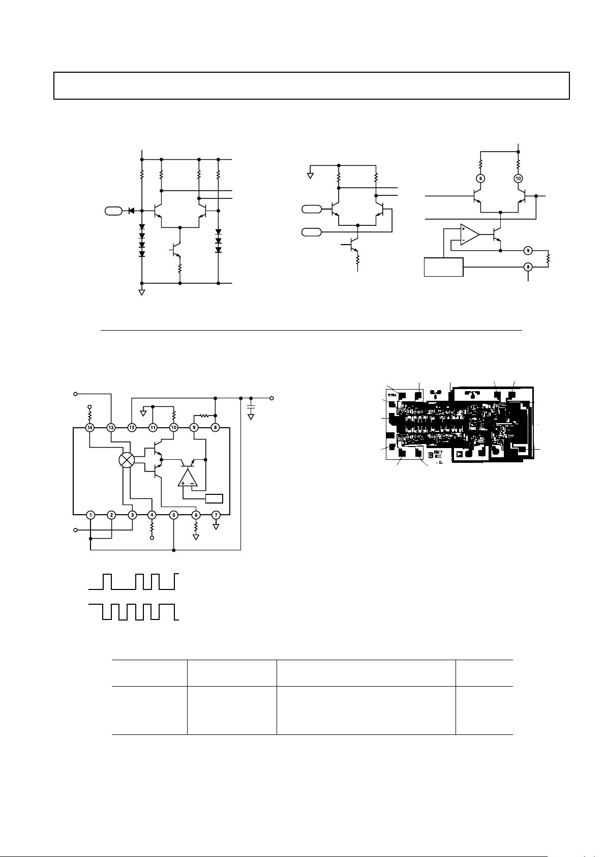
INPUT/OUTPUT EQUIVALENT CIRCUITS
(Based on DIP Pinouts)
TTL Input ECL Input Output
DIE LAYOUT AND MECHANICAL INFORMATION
REFERENCE IN (–VS)+VS (GND) OUTPUT
R
SET
GND (–VS)
+V
S
(GND)
OUTPUT
VCO IN (–V
S
)GND (VCO IN)
GND (VCO IN)
VS (–VS)
GND (–V
S
)
GND (REFERENCE IN)
GND (REFERENCE IN)
Die Dimensions . . . . . . . . . . . . . . . . . 63 × 118 × 16 (±2) mils
Pad Dimensions . . . . . . . . . . . . . . . . . . . . . . . . . . . . 4 × 4 mils
Metalization . . . . . . . . . . . . . . . . . . . . . . . . . . . . . . Aluminum
Backing . . . . . . . . . . . . . . . . . . . . . . . . . . . . . . . . . . . . . None
Substrate Potential . . . . . . . . . . . . . . . . . . . . . . . . . . . . . . –V
S
Passivation . . . . . . . . . . . . . . . . . . . . . . . . . . . . . . . . . . Nitride
Die Attach . . . . . . . . . . . . . . . . . . . . . . . . . . . . . Gold Eutectic
Bond Wire . . . . . . . . 1.25 mil Aluminum; Ultrasonic Bonding
ORDERING GUIDE
Temperature Package Package
Model Ranges Descriptions Options
AD9901KQ 0°C to +70°C 14-Lead Cerdip Q-14
AD9901KP 0°C to +70°C 20-Lead Plastic Leaded Chip Carrier P-20A
AD9901TQ/883
1
–55°C to +125°C 14-Lead Cerdip Q-14
AD9901TE/883
1
–55°C to +125°C 20-Terminal Ceramic Leadless Chip Carrier E-20A
NOTE
1
For specifications, refer to Analog Devices Military Products Databook.
AD9901 BURN-IN CIRCUIT
(Based on DIP ECL Pinouts)
REG
V
MID
1kV
180V
DA3
DA2
V
MID
1kV
180V
50V
0.01mF
–V
S
(–5.2V)
AD9901
ECL HIGH
ECL LOW
DA2
ECL HIGH
ECL LOW
DA3
ALL RESISTORS 65%
ALL CAPACITORS 620%
ALL SUPPLY VOLTAGES 65%
V
MID
= –1.3V 65%
STATIC: DA2 = ECL HIGH; DA3 = ECL LOW
DYNAMIC: ECL HIGH
5/12
+5.0V
VCO/REF, INPUT
4/13
3/14
–5.2V
VCO/REF, INPUT
VCO/REF, INPUT
0.47V
REFERENCE
TTL MODE = GROUND
ECL MODE = V
S
(–5.2V)
R
SET
TTL MODE = +VS (+5.0V)
ECL MODE = GROUND
 Loading...