

12-Bit, 20 MSPS/40 MSPS/65 MSPS
FEATURES
Ultralow power
85 mW at 20 MSPS
135 mW at 40 MSPS
190 mW at 65 MSPS
SNR = 66 dBc to Nyquist at 65 MSPS
SFDR = 80 dBc to Nyquist at 65 MSPS
DNL = ±0.7 LSB
Differential input with 500 MHz bandwidth
Flexible analog input: 1 V p-p to 4 V p-p range
Offset binary, twos complement, or gray code data formats
Output enable pin
2-step power-down
Full power-down and sleep mode
Clock duty cycle stabilizer
APPLICATIONS
Ultrasound and medical imaging
Battery-powered instruments
Hand-held scope meters
Low cost digital oscilloscopes
Low power digital still cameras and copiers
Low power communications
GENERAL DESCRIPTION
The AD9237 is a family of monolithic, single 3 V supply, 12-bit,
20 MSPS/40 MSPS/65 MSPS analog-to-digital converters
(ADC). This family features a high performance sample-andhold amplifier (SHA) and voltage reference. The AD9237 uses a
multistage differential pipelined architecture with output error
correction logic to provide 12-bit accuracy at 20 MSPS/
40 MSPS/65 MSPS data rates and guarantees no missing codes
over the full operating temperature range.
With significant power savings over previously available ADCs,
the AD9237 is suitable for applications in imaging and medical
ultrasound.
Fabricated on an advanced CMOS process, the AD9237 is
available in a 32-lead LFCSP and is specified over the industrial
temperature range (−40°C to +85°C).
3 V Low Power A/D Converter
AD9237
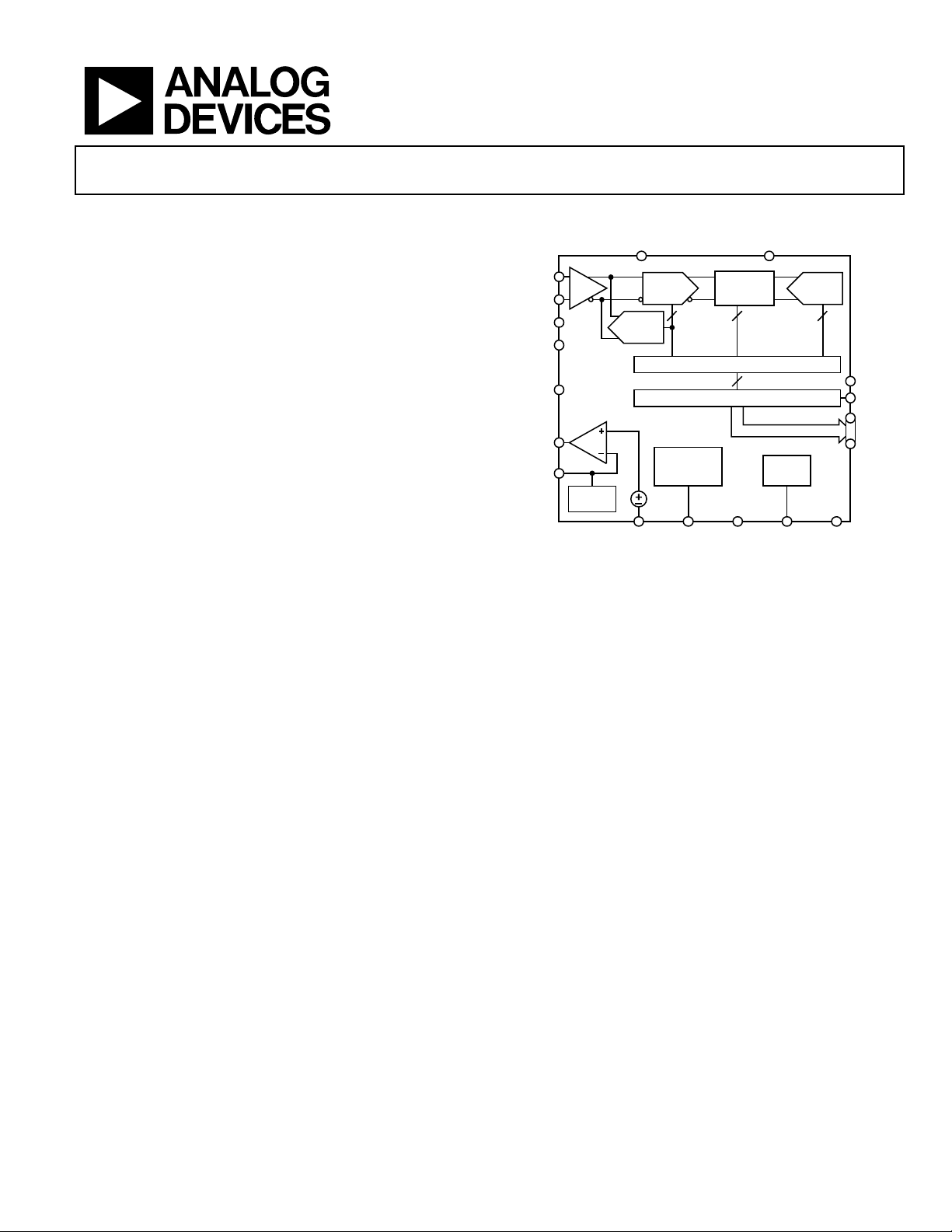
FUNCTIONAL BLOCK DIAGRAM
AVDD
VIN+
VIN–
REFT
REFB
MODE2
VREF
SENSE
SHA
REF
SELECT
A/D
AGND
MDAC1
4 15
CORRECTION LOGIC
OUTPUT BUFFERS
AD9237
CLOCK
DUTY CYCLE
STABILIZER
0.5V
CLK PDWN MODE
Figure 1.
PRODUCT HIGHLIGHTS
1. Operating at 65 MSPS, the AD9237 consumes a low 190 mW
at 65 MSPS, 135 mW at 40 MSPS, and 85 mW at 20 MSPS.
2. Power scaling reduces the operating power further when
running at lower speeds.
3. The AD9237 operates from a single 3 V power supply and
features a separate digital output driver supply to
accommodate 2.5 V and 3.3 V logic families.
4. The patented SHA input maintains excellent performance
for input frequencies beyond Nyquist and can be configured
for single-ended or differential operation.
5. The AD9237 is optimized for selectable and flexible input
ranges from 1 V p-p to 4 V p-p.
6. An output enable pin allows for multiplexing of the outputs.
7. Two-step power-down supports a standby mode in addition
to a power-down mode.
8. The OTR output bit indicates when the signal is beyond the
selected input range.
9. The clock duty cycle stabilizer (DCS) maintains converter
performance over a wide range of clock pulse widths.
DRVDD
10-STAGE
1 1/2-BIT
PIPELINE
12
MODE
SELECT
A/D
3
OE
OTR
D11
D0
DGND
05455-001
Rev. A
Information furnished by Analog Devices is believed to be accurate and reliable. However, no
responsibility is assumed by Analog Devices for its use, nor for any infringements of patents or other
rights of third parties that may result from its use. Specifications subject to change without notice. No
license is granted by implication or otherwise under any patent or patent rights of Analog Devices.
Trademarks and registered trademarks are the property of their respective owners.
One Technology Way, P.O. Box 9106, Norwood, MA 02062-9106, U.S.A.
Tel: 781.329.4700 www.analog.com
Fax: 781.461.3113 © 2005–2010 Analog Devices, Inc. All rights reserved.

AD9237
TABLE OF CONTENTS
Features .............................................................................................. 1
Pin Configuration and Function Descriptions ..............................8
Applications ....................................................................................... 1
Functional Block Diagram .............................................................. 1
General Description ......................................................................... 1
Product Highlights ........................................................................... 1
Revision History ............................................................................... 2
Specifications ..................................................................................... 3
DC Specifications ......................................................................... 3
Digital Specifications ................................................................... 4
AC Specifications .......................................................................... 4
Switching Specifications .............................................................. 5
Timing Diagram ............................................................................... 6
Absolute Maximum Ratings ............................................................ 7
ESD Caution .................................................................................. 7
REVISION HISTORY
Terminology .......................................................................................9
Equivalent Circuits ......................................................................... 10
Typical Performance Characteristics ........................................... 11
Applying the AD9237 .................................................................... 16
Theory of Operation .................................................................. 16
Analog Input and Reference Overview ................................... 16
Voltage Reference ....................................................................... 18
Clock Input Considerations ...................................................... 19
Power Dissipation, Power Scaling, and Standby Mode ......... 19
Digital Outputs ........................................................................... 21
Outline Dimensions ....................................................................... 22
Ordering Guide .......................................................................... 22
5/10—Rev. 0 to Rev. A
Changes to Product Highlights Section ......................................... 1
Changes to Pipeline Delay Parameter in Table 4 .......................... 5
Changes to Figure 2 .......................................................................... 6
Changes to Figure 3 and Table 6 ..................................................... 8
10/05—Revision 0: Initial Version
Rev. A | Page 2 of 24

AD9237
SPECIFICATIONS
DC SPECIFICATIONS
AVDD = 3 V, DRVDD = 2.5 V, maximum sample rate, 2 V p-p differential input, −0.5 dBFS input, 1.0 V internal reference, T
unless otherwise noted.
Table 1.
AD9237BCP-20 AD9237BCP-40 AD9237BCP-65
Parameter Min Typ Max Min Typ Max Min Typ Max Unit
RESOLUTION 12 12 12 Bits
ACCURACY
No Missing Codes Guaranteed 12 12 12 Bits
Offset Error ±1.30 ±1.95 ±1.30 ±1.95 ±1.30 ±1.95 % FSR
Gain Error1 ±0.70 ±2.10 ±0.75 ±2.10 ±1.05 ±2.25 % FSR
Differential Nonlinearity (DNL)2 ±0.70 ±0.95 ±0.70 ±0.95 −1.00 ±0.70 +1.25 LSB
Integral Nonlinearity (INL)2 ±0.90 ±1.35 ±0.90 ±1.35 ±0.90 ±2.00 LSB
TEMPERATURE DRIFT
Offset Error ±2 ±2 ±2 ppm/°C
Gain Error1 ±12 ±12 ±12 ppm/°C
INTERNAL VOLTAGE REFERENCE
Output Voltage Error (1 V Mode) ±5 ±25 ±5 ±25 ±5 ±25 mV
Load Regulation @ 1.0 mA 0.8 0.8 0.8 mV
Output Voltage Error (0.5 V Mode) ±2.5 ±2.5 ±2.5 mV
Load Regulation @ 0.5 mA 0.1 0.1 0.1 mV
Reference Input Resistance 7 7 7 kΩ
INPUT REFERRED NOISE
VREF = 0.5 V 1.35 1.35 1.35 LSB rms
VREF = 1.0 V 0.70 0.70 0.70 LSB rms
ANALOG INPUT
Input Span
VREF = 0.5 V; MODE2 = 0 V 1 1 1 V p-p
VREF = 1.0 V; MODE2 = 0 V 2 2 2 V p-p
VREF = 0.5 V; MODE2 = AVDD 2 2 2 V p-p
VREF = 1.0 V; MODE2 = AVDD 4 4 4 V p-p
Input Capacitance3 7 7 7 pF
POWER SUPPLIES
Supply Voltages
AVDD 2.7 3.0 3.6 2.7 3.0 3.6 2.7 3.0 3.6 V
DRVDD 2.25 2.5 3.6 2.25 2.5 3.6 2.25 2.5 3.6 V
Supply Current
IAVDD2 30.5 45.5 64.5 mA
IDRVDD2 3.0 4.5 5.5 mA
PSRR ±0.01 ±0.01 ±0.01 % FSR
POWER CONSUMPTION
DC Input4 85 135 190 mW
Sine Wave Input2 100 120 150 180 210 270 mW
Power-Down Mode 1 1 1 mW
Standby Power 20 20 20 mW
1
Gain error and gain temperature coefficient are based on the ADC only (with a fixed 1.0 V external reference).
2
Measured at maximum clock rate, fIN = 2.4 MHz, full-scale sine wave, with approximately 5 pF loading on each output bit.
3
Input capacitance refers to the effective capacitance between one differential input pin and AGND. Refer to for the equivalent analog input structure. Figure 4
4
Measured with dc input at maximum clock rate.
MIN
to T
MAX
,
Rev. A | Page 3 of 24

AD9237
DIGITAL SPECIFICATIONS
Table 2.
AD9237BCP-20 AD9237BCP-40 AD9237BCP-65
Parameter Min Typ Max Min Typ Max Min Typ Max Unit
LOGIC INPUTS
High Level Input Voltage 2.0 2.0 2.0 V
Low Level Input Voltage 0.8 0.8 0.8 V
High Level Input Current –10 +10 –10 +10 –10 +10 μA
Low Level Input Current –10 +10 –10 +10 –10 +10 μA
Input Capacitance 2 2 2 pF
LOGIC OUTPUTS1
DRVDD = 3.3 V
High-Level Output Voltage (IOH = 50 μA) 3.29 3.29 3.29 V
High-Level Output Voltage (IOH = 0.5 mA) 3.25 3.25 3.25 V
Low-Level Output Voltage (IOL = 1.6 mA) 0.2 0.2 0.2 V
Low-Level Output Voltage (IOL = 50 μA) 0.05 0.05 0.05 V
DRVDD = 2.5 V
High-Level Output Voltage (IOH = 50 μA) 2.49 2.49 2.49 V
High-Level Output Voltage (IOH = 0.5 mA) 2.45 2.45 2.45 V
Low-Level Output Voltage (IOL = 1.6 mA) 0.2 0.2 0.2 V
Low-Level Output Voltage (IOL = 50 μA) 0.05 0.05 0.05 V
1
Output voltage levels measured with 5 pF load on each output.
AC SPECIFICATIONS
AVDD = 3 V, DRVDD = 2.5 V, maximum sample rate, 2 V p-p differential input, AIN = –0.5 dBFS, 1.0 V internal reference, T
unless otherwise noted.
Table 3.
AD9237BCP-20 AD9237BCP-40 AD9237BCP-65
Parameter Min Typ Max Min Typ Max Min Typ Max Unit
SIGNAL-TO-NOISE RATIO (SNR)
f
= 2.4 MHz 66.8 66.5 66.5 dBc
INPUT
f
= 9.7 MHz 65.6 66.6 dBc
INPUT
f
= 19.6 MHz 65.3 66.6 dBc
INPUT
f
= 34.2 MHz 64.0 66.1 dBc
INPUT
f
= 70 MHz 66.0 66.3 65.9 dBc
INPUT
SIGNAL-TO-NOISE RATIO AND DISTORTION (SINAD)
f
= 2.4 MHz 66.7 66.4 66.3 dBc
INPUT
f
= 9.7 MHz 65.1 66.5 dBc
INPUT
f
= 19.6 MHz 64.4 66.4 dBc
INPUT
f
= 34.2 MHz 63.5 65.8 dBc
INPUT
f
= 70 MHz 65.6 65.8 65.2 dBc
INPUT
EFFECTIVE NUMBER OF BITS (ENOB)
f
= 9.7 MHz 10.8 Bits
INPUT
f
= 19.6 MHz 10.7 Bits
INPUT
f
= 34.2 MHz 10.6 Bits
INPUT
MIN
to T
MAX
,
Rev. A | Page 4 of 24

AD9237
AD9237BCP-20 AD9237BCP-40 AD9237BCP-65
Parameter Min Typ Max Min Typ Max Min Typ Max Unit
SPURIOUS-FREE DYNAMIC RANGE (SFDR)
f
= 2.4 MHz 88.0 83.5 85.5 dBc
INPUT
f
= 9.7 MHz 72.4 87.5 dBc
INPUT
f
= 19.6 MHz 72.2 82.4 dBc
INPUT
f
= 34.2 MHz 69.4 80.1 dBc
INPUT
f
= 70 MHz 80.5 77.9 74.9 dBc
INPUT
WORST HARMONIC (SECOND OR THIRD)
f
= 2.4 MHz −88.0 −83.5 −85.5 dBc
INPUT
f
= 9.7 MHz −72.4 −87.5 dBc
INPUT
f
= 19.6 MHz −72.2 −82.4 dBc
INPUT
f
= 34.2 MHz −69.4 −80.1 dBc
INPUT
f
= 70 MHz −80.5 −77.9 −74.9 dBc
INPUT
WORST OTHER SPUR
f
= 2.4 MHz −90 −90 −90 dBc
INPUT
f
= 9.7 MHz −73.4 −90 dBc
INPUT
f
= 19.6 MHz −73.1 −90 dBc
INPUT
f
= 34.2 MHz −72.0 −90 dBc
INPUT
f
= 70 MHz −90 −90 −90 dBc
INPUT
SWITCHING SPECIFICATIONS
Table 4.
AD9237BCP-20 AD9237BCP-40 AD9237BCP-65
Parameter Min Typ Max Min Typ Max Min Typ Max Unit
CLK INPUT PARAMETERS
Maximum Conversion Rate 20 40 65 MSPS
Minimum Conversion Rate 1 1 1 MSPS
CLK Period 50.0 25.0 15.4 ns
CLK Pulse Width High1 15.0 8.8 6.2 ns
CLK Pulse Width Low1 15.0 8.8 6.2 ns
DATA OUTPUT PARAMETERS
Output Delay (tPD)2 3.5 3.5 3.5 ns
Pipeline Delay (Latency) 9 9 9 Cycles
Output Enable Time 6 6 6 ns
Output Disable Time 3 3 3 ns
Aperture Delay (tA) 1.0 1.0 1.0 ns
Aperture Uncertainty (Jitter, tJ) 0.5 0.5 0.5 ps rms
Wake-Up Time (Sleep Mode)3 3.0 3.0 3.0 ms
Wake-Up Time (Standby Mode)3 3.0 3.0 3.0 μs
OUT-OF-RANGE RECOVERY TIME 1 1 2 Cycles
1
With duty cycle stabilizer enabled.
2
Output delay is measured from CLK 50% transition to DATA 50% transition, with 5 pF load on each output.
3
Wake-up time is dependent on value of decoupling capacitors; typical values shown with 0.1 μF and 10 μF capacitors on REFT and REFB.
Rev. A | Page 5 of 24
AD9237
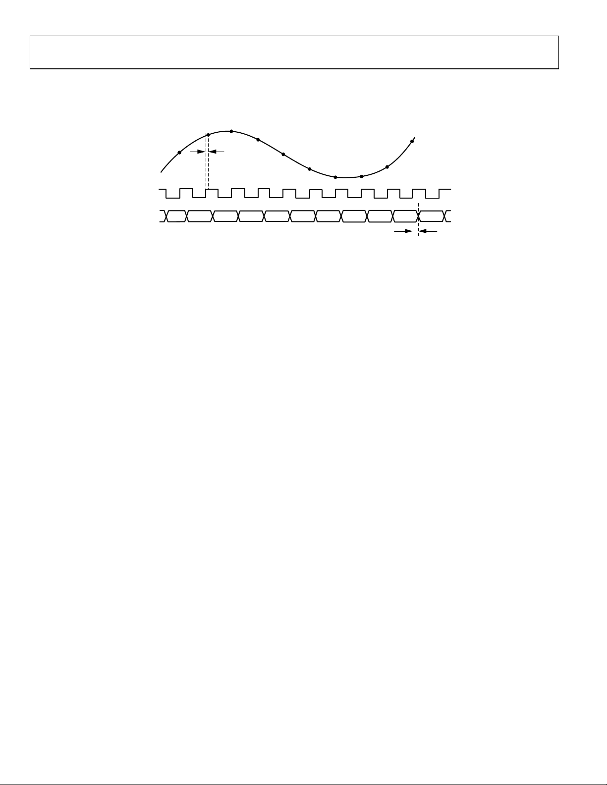
TIMING DIAGRAM
N+1
ANALOG
INPUT
CLK
N
N–1
N+2
t
A
N+3
N+4
N+5 N+6
N+8
N+7
DATA
OUT
N–10 N–9 N–8 N–7 N–6 N–5 N–4 N–3 N–2 N–1
N–11
t
PD
05455-002
Figure 2. Timing Diagram
Rev. A | Page 6 of 24
AD9237
ABSOLUTE MAXIMUM RATINGS
Table 5.
With
Pin Name
ELECTRICAL
AVDD AGND –0.3 +3.9 V
DRVDD DGND –0.3 +3.9 V
AGND DGND –0.3 +0.3 V
AVDD DRVDD –3.9 +3.9 V
Digital
Outputs, OE
CLK, MODE,
MODE2
VIN+, VIN– AGND –0.3 AVDD + 0.3 V
VREF AGND –0.3 AVDD + 0.3 V
SENSE AGND –0.3 AVDD + 0.3 V
REFB, REFT AGND –0.3 AVDD + 0.3 V
PDWN AGND –0.3 AVDD + 0.3 V
ENVIRONMENTAL1
Operating Temperature –40 +85 °C
Junction Temperature 150 °C
Lead Temperature (10 sec) 300 °C
Storage Temperature –65 +150 °C
1
Typical thermal impedances (32-lead LFCSP), θJA = 32.5°C/W, θJC = 32.71°C/W.
These measurements were taken on a 4-layer board in still air, in accordance
with EIA/JESD51-1.
Respect to Min Max Unit
DGND –0.3 DRVDD + 0.3 V
AGND −0.3 AVDD + 0.3 V
Stresses above those listed under Absolute Maximum Ratings
may cause permanent damage to the device. This is a stress
rating only; functional operation of the device at these or any
other conditions above those indicated in the operational
section of this specification is not implied. Exposure to absolute
maximum rating conditions for extended periods may affect
device reliability.
Absolute maximum ratings are limiting values to be applied
individually and beyond which the serviceability of the circuit
may be impaired. Functional operability is not necessarily
implied. Exposure to absolute maximum rating conditions for
an extended period may affect device reliability.
ESD CAUTION
Rev. A | Page 7 of 24

AD9237
PIN CONFIGURATION AND FUNCTION DESCRIPTIONS
DD
AGND
AV
32
AVDD
VIN–
VIN+
REFT
AGND
31
30
REFB
29
28
27
26
25
14
D7
15
16
DGND
DRVDD
24 VREF
23 SENSE
22 MODE
21 OTR
20 D11 (MSB)
19 D10
18 D9
17 D8
05455-003
1MODE2
PIN 1
2CLK
INDICATOR
3OE
4PDWN
AD9237
5GC
TOP VIEW
6DNC
(Not to Scale)
7D0 (LSB)
8D1
9
11
10
12
13
D2
D3
D4
D5
D6
NOTES
1. DNC = DO NOT CONNECT.
2. IT I S RECOMMENDED T HAT THE EXPO SED PADDLE
BE SOLDEREDTO THE GROUND PLANE.
Figure 3. Pin Configuration
Table 6. Pin Function Descriptions
Pin Number Mnemonic Description
1 MODE2 SHA Gain Select and Power Scaling Control (see Tabl e 8).
2 CLK Clock Input Pin.
3 OE Output Enable Pin (Active Low).
4 PDWN Power-Down Function Selection (see Table 9).
5 GC Gray Code Control (Active High).
6 DNC Do Not Connect.
7 to 14, 17 to 20 D0 (LSB) to D11 (MSB) Data Output Bits.
15 DGND Digital Output Ground.
16 DRVDD
Digital Output Driver Supply. Must be decoupled to DGND with a minimum 0.1 μF capacitor.
Recommended decoupling is 0.1 μF in parallel with 10 μF.
21 OTR Out-of-Range Indicator.
22 MODE Data Format and Clock Duty Cycle Stabilizer (DCS) Mode Selection (see Table 1 0).
23 SENSE Reference Mode Selection (see Table 7).
24 VREF Voltage Reference Input/Output (see Table 7).
25 REFB Differential Reference (−). Must be decoupled to REFT with a minimum 10 μF capacitor.
26 REFT Differential Reference (+).
27, 32 AVDD
Analog Power Supply. Must be decoupled to AGND with a minimum 0.1 μF capacitor.
Recommended decoupling is 0.1 μF in parallel with 10 μF.
28, 31 AGND Analog Ground.
29 VIN+ Analog Input Pin (+).
30 VIN− Analog Input Pin (−).
EP
It is recommended that the exposed paddle be soldered to the ground plane. There is an
increased reliability of the solder joints and maximum thermal capability of the package is
achieved with exposed paddle soldered to the customer board.
Rev. A | Page 8 of 24

AD9237
TERMINOLOGY
Analog Bandwidth (Full Power Bandwidth)
The analog input frequency at which the spectral power of the
fundamental frequency (as determined by the FFT analysis) is
reduced by 3 dB.
Signal-To-Noise and Distortion (SINAD)
The ratio of the rms signal amplitude to the rms value of the
sum of all other spectral components below the Nyquist
frequency, including harmonics but excluding dc.
1
Aperture Delay (t
)
A
The delay between the 50% point of the rising edge of the clock
and the instant at which the analog input is sampled.
Aperture Jitter (t
)
J
The sample-to-sample variation in aperture delay.
Integral Nonlinearity (INL)
The deviation of each individual code from a line drawn from
negative full scale through positive full scale. The point used
as negative full scale occurs ½ LSB before the first code
transition. Positive full scale is defined as a level 1½ LSBs
beyond the last code transition. The deviation is measured
from the middle of each particular code to the true straight line.
Differential Nonlinearity (DNL, No Missing Codes)
An ideal ADC exhibits code transitions that are exactly 1 LSB
apart. DNL is the deviation from this ideal value. Guaranteed
no missing codes to 12-bit resolution indicates that all 4096
codes must be present over all operating ranges.
Offset Error
The major carry transition should occur for an analog value
½ LSB below VIN+ = VIN–. Offset error is defined as the
deviation of the actual transition from that point.
Gain Error
The first code transition should occur at an analog value
½ LSB above negative full scale. The last transition should occur
at an analog value 1½ LSB below the positive full scale. Gain
error is the deviation of the actual difference between first and
last code transitions and the ideal difference between first and
last code transitions.
Temp er at u re D ri ft
The temperature drift for offset error and gain error specifies
the maximum change from the initial (25°C) value to the value
at T
MIN
or T
MAX
.
Power Supply Rejection Ratio
The change in full scale from the value with the supply at the
minimum limit to the value with the supply at its maximum
limit.
Total Harmonic Distortion (THD)
1
The ratio of the rms sum of the first six harmonic components
to the rms value of the measured input signal.
Effective Number of Bits (ENOB)
The effective number of bits for a device for sine wave inputs
at a given input frequency can be calculated directly from its
measured SINAD using the following formula:
ENOB = (SINAD
Signal-to-Noise Ratio (SNR)
− 1.76)/6.02
dBFS
1
The ratio of the rms signal to the rms value of the sum of all
other spectral components below the Nyquist frequency,
excluding the first six harmonics and dc.
Spurious-Free Dynamic Range (SFDR)
1
SFDR is the difference in dB between the rms amplitude of the
input signal and the rms value of the peak spurious signal. The
peak spurious signal may not be an harmonic.
Two -Tone SFDR
1
The ratio of the rms value of either input tone to the rms value
of the peak spurious component. The peak spurious component
may or may not be an IMD product.
Clock Pulse Width and Duty Cycle
Pulse width high is the minimum amount of time that the clock
pulse should be left in the Logic 1 state to achieve rated
performance. Pulse width low is the minimum time the clock
pulse should be left in the low state. At a given clock rate, these
specifications define an acceptable clock duty cycle.
Minimum Conversion Rate
The clock rate at which the SNR of the lowest analog signal
frequency drops by no more than 3 dB below the guaranteed
limit.
Maximum Conversion Rate
The clock rate at which parametric testing is performed.
Output Propagation Delay (t
)
PD
The delay between the clock logic threshold and the time when
all bits are within valid logic levels.
Out-of-Range Recovery Time
The time it takes the ADC to reacquire the analog input after a
transition from 10% above positive full scale to 10% above
negative full scale, or from 10% below negative full scale to 10%
below positive full scale.
1
AC specifications may be reported in dBc (degrades as signal levels are
lowered) or in dBFS (always related back to converter full scale).
Rev. A | Page 9 of 24

AD9237
V
EQUIVALENT CIRCUITS
AVDD
IN+, VIN–
05455-004
Figure 4. Equivalent Analog Input Circuit
MODE,
MODE2,
GC, OE
375Ω
70kΩ
05455-005
Figure 5. Equivalent MODE, MODE2, GC, OE Input Circuit
DRVDD
D11–D0,
OTR
Figure 6. Equivalent Digital Output Circuit
CLK,
PDWN
375Ω
Figure 7. Equivalent CLK, PDWN Input Circuit
05455-006
05455-007
Rev. A | Page 10 of 24

AD9237
TYPICAL PERFORMANCE CHARACTERISTICS
AVDD = 3.0 V, DRVDD = 2.5 V, maximum sample rate with DCS disabled, TA = 25°C, 2 V p-p differential input, AIN = –0.5 dBFS,
VREF = 1.0 V internal, FFT length 16 K, unless otherwise noted.
0
–20
SNR = 66.9dBc
SFDR = 87.0dBc
90
85
SFDR
–40
–60
–80
AMPLITUDE (dBFS)
–100
–120
016842
FREQUENCY (MHz)
05455-008
0
Figure 8. AD9237-20 10 MHz FFT
0
SNR = 66.8dBc
SFDR = 83.1dBc
–20
–40
–60
–80
AMPLITUDE (dBFS)
–100
–120
020
FREQUENCY (MHz)
12 16841810 1462
05455-009
Figure 9. AD9237-40 20 MHz FFT
0
–20
–40
SNR = 66.0dBc
SFDR = 78.6dBc
80
75
SNR/SFDR (dBc)
70
65
60
10.0 20.017.515.012.5
Figure 11. AD9237-20 SNR/SFDR vs. Clock Frequency with fIN = 10 MHz
90
85
80
75
SNR/SFDR (dBc)
70
65
20 40353025
Figure 12. AD9237-40 SNR/SFDR vs. Clock Frequency with fIN = 20 MHz
90
85
80
SNR
05455-011
CLOCK FREQUENCY (MSPS)
SFDR
SNR
05455-012
CLOCK FREQUENCY (MSPS)
SFDR
AMPLITUDE (dBFS)
–60
–80
–100
–120
0 30 32.5252015105
FREQUENCY (MHz)
Figure 10. AD9237-65 70 MHz FFT
05455-010
Rev. A | Page 11 of 24
75
SNR/SFDR (dBc)
70
SNR
65
60
40 6555 605045
CLOCK FREQUENCY (MSPS)
Figure 13. AD9237-65 SNR/SFDR vs. Clock Frequency with fIN = 35 MHz
05455-013

AD9237
0
–20
–40
SNR = 65.6dBc
SFDR = 67.1dBc
90
85
80
75
SFDR DCS
ENABLED
SFDR DCS
DISABLED
–60
–80
AMPLITUDE (dBc)
–100
–120
0 30 32.5252015105
FREQUENCY (MHz)
Figure 14. AD9237-65 100 MHz FFT
90
80
70
60
50
SNR/SFDR (dBc and dBFS)
40
30
–30 0–5–10–15–20–25
SFDR dBFS 2V p-p
SNR dBFS 2V p-p
SNR dBFS 4V p-p
SFDR dBc 2V p-p
SFDR dBFS 4V p-p
SFDR dBc 4V p-p
SNR dBc 2V p-p
SNR dBc 4V p-p
INPUT AMPLITUDE (dBFS)
Figure 15. AD9237-65 SNR/SFDR vs. Input Amplitude with fIN = 35 MHz
100
SFDR dBFS 2V p-p
90
05455-014
05455-017
SNR/SFDR (dBc)
70
65
60
55
50
30 7065605550454035
DUTY CYCLE (%)
SNR DCS ENABLED
SNR DCS DISABLED
Figure 17. SNR/SFDR vs. Clock Duty Cycle
90
80
70
60
50
SNR/SFDR (dBc and dBFS)
40
30
–30 0–5–10–15–20–25
SFDR dBFS 2V p-p
SFDR dBFS 1V p-p
SNR dBFS 2V p-p
SNR dBFS 1V p-p
SNR dBc 2V p-p
SFDR dBc 2V p-p
SFDR dBc 1V p-p
SNR dBc 1V p-p
INPUT AMPLITUDE (dBFS)
Figure 18. AD9237-65 SNR/SFDR vs. Input Amplitude with fIN = 35 MHz
100
SFDR dBFS 2V p-p
90
05455-030
05455-018
80
SFDR dBFS 1V p-p
70
60
50
SNR/SFDR (dBc and dBFS)
40
30
–30 0–5–10–15–20–25
SNR dBFS 1V p-p
SFDR dBc 2V p-p
SFDR dBc 1V p-p
SNR dBFS 2V p-p
SNR dBc 2V p-p
SNR dBc 1V p-p
INPUT AMPLITUDE (dBFS)
Figure 16. AD9237-40 SNR/SFDR vs. Input Amplitude with fIN = 20 MHz
Rev. A | Page 12 of 24
05455-019
80
SFDR dBFS 1V p-p
70
60
50
SNR/SFDR (dBc and dBFS)
40
30
–30 0–5–10–15–20–25
SFDR dBc 2V p-p
SNR dBFS 1V p-p
SNR dBFS 2V p-p
SNR dBc 2V p-p
SNR dBc 1V p-p
INPUT AMPLITUDE (dBFS)
SFDR dBc 1V p-p
Figure 19. AD9237-20 SNR/SFDR vs. Input Amplitude with fIN = 10 MHz
05455-020

AD9237
0
SNR = 67.0dBFS
SFDR = 87.8dBFS
–20
–40
–60
–80
AMPLITUDE (dBc)
–100
–120
0 30 32.5252015105
FREQUENCY (MHz)
Figure 20. AD9237-65 Two-Tone FFT, f
0
–20
–40
–60
–80
AMPLITUDE (dBc)
–100
–120
0215105
FREQUENCY (MHz)
Figure 21. AD9237-40 Two-Tone FFT
= 45 MHz, f
f
AMPLITUDE (dBFS)
–20
–40
–60
–80
–100
–120
IN1
0
03252015105
IN2
FREQUENCY (MHz)
Figure 22. AD9237-65 Two-Tone FFT, f
= 45 MHz, f
IN1
= 46 MHz
= 69 MHz, f
IN1
= 46 MHz
IN2
SNR = 67.2dBFS
SFDR = 88.3dBFS
SNR = 66.9dBFS
SFDR = 84.1dBFS
0
= 70 MHz
IN2
05455-095
05455-021
0
05455-094
100
90
SFDR dBFS
80
SNR dBFS
70
60
SFDR dBc
50
SNR/SFDR (dBc and dBFS)
40
SNR dBc
30
–30 –10 –6.5–15–20–25
INPUT AMPLITUDE (AIN)
Figure 23. AD9237-65 Two-Tone SNR/SFDR , vs. Analog Input with
100
90
80
70
60
50
SNR/SFDR (dBc and dBFS)
40
30
–30 –10 –6.5–15–20–25
SFDR dBFS
SNR dBFS
SFDR dBc
SNR dBc
= 45 MHz, f
f
IN1
INPUT AMPLITUDE (AIN)
= 46 MHz
IN2
Figure 24. AD9237-40 Two-Tone SNR/SFDR , vs. Analog Input with
= 45 MHz, f
f
IN1
100
90
SFDR dBFS
80
SNR dBFS
70
60
SFDR dBc
50
SNR/SFDR (dBc and dBFS)
40
SNR dBc
30
–30 –10 –6.5–15–20–25
INPUT AMPLITUDE (AIN)
= 46 MHz
IN2
Figure 25. AD9237-65 Two-Tone SNR/SFDR vs. Analog Input with
= 69 MHz, f
f
IN1
= 70 MHz
IN2
05455-024
05455-025
05455-098
Rev. A | Page 13 of 24

AD9237
0
–20
–40
–60
–80
AMPLITUDE (dBc)
–100
–120
90
0215105
FREQUENCY (MHz)
Figure 26. AD9237-40 Two-Tone FFT
= 69 MHz, f
f
IN1
= 70 MHz
IN2
SNR = 67.1dBFS
SFDR = 87.3dBFS
05455-026
0
100
90
SFDR dBFS
80
SNR dBFS
70
60
SFDR dBc
50
SNR/SFDR (dBc and dBFS)
40
SNR dBc
30
–30 –10 –6.5–15–20–25
INPUT AMPLITUDE (AIN)
Figure 29. AD9237-40 Two-Tone SNR/SFDR vs. Analog Input with
= 69 MHz, f
f
IN1
90
= 70 MHz
IN2
05455-097
85
SFDR
80
75
70
SNR/SFDR (dBc)
SNR
65
60
55
0 125100755025
INPUT FREQUENCY (MHz)
Figure 27. AD9237-65 SNR/SFDR vs. Input Frequency
1.00
0.75
0.50
0.25
0
INL (LSB)
–0.25
–0.50
05455-015
SNR/SFDR (dBc)
85
80
75
70
65
60
55
0 125100755025
SFDR
SNR
INPUT FREQUENCY (MHz)
Figure 30. AD9237-40 SNR/SFDR vs. Input Frequency
1.00
0.75
0.50
0.25
0
DNL (LSB)
–0.25
–0.50
05455-016
–0.75
–1.00
0 4096358430722560204815361024512
CODE
Figure 28. Typical INL
05455-032
Rev. A | Page 14 of 24
–0.75
–1.00
0 4096358430722560204815361024512
05455-035
CODE
Figure 31. Typical DNL

AD9237
67.5
90
67.0
AD9237-20
AD9237-40
66.5
66.0
SINAD (dBc)
65.5
65.0
10 20 7060504030
CLOCK FREQUENCY (MSPS)
AD9237-65
Figure 32. AD9237 SINAD/ENOB vs. Clock Frequency with fIN = Nyquist
10.83
10.75
10.67
10.59
10.50
ENOB (Bits)
05455-062
85
80
75
SNR/SFDR (dBc)
70
65
60
–40 –20 85806040200
SNR
SFDR
TEMPERATURE (°C)
Figure 33. AD9237-65 SNR/SFDR vs. Temperature with fIN = 32.5MHz
05455-063
Rev. A | Page 15 of 24

AD9237
V
V
APPLYING THE AD9237
THEORY OF OPERATION
The AD9237 uses a calibrated, 11-stage pipeline architecture
with a patented input SHA implemented. Each stage of the
pipeline, excluding the last, consists of a low resolution flash
ADC connected to a switched capacitor digital-to-analog
converter (DAC) and an interstage residue amplifier (MDAC).
The MDAC magnifies the difference between the reconstructed
DAC output and the flash input for the next stage in the
pipeline. One bit of redundancy is used in each stage to facilitate
digital correction of flash errors. The last stage consists of a
flash ADC.
The pipelined architecture permits the first stage to operate on a
new input sample, while the remaining stages operate on preceding
samples. While the converter captures a new input sample every
clock cycle, it takes eight clock cycles for the conversion to be
fully processed and to appear at the output, as shown in Figure 2.
The input stage contains a differential SHA that can be ac- or
dc-coupled in differential or single-ended modes. The outputstaging block aligns the data, carries out the error correction,
and passes the data to the output buffers. The output buffers
are powered from a separate supply, allowing adjustment of
the output voltage swing. During power-down and stand-by
operation, the output buffers go into a high impedance state.
In addition, a small shunt capacitor placed across the inputs
provides dynamic charging currents. This passive network
creates a low-pass filter at the ADC’s input; therefore, the
precise values are dependent on the application. In IF undersampling applications, the shunt capacitor(s) should be reduced
or removed depending on the input frequency. In combination
with the driving source impedance, the capacitors limit the
input bandwidth.
90
80
70
60
SNR/SFDR (dBc)
50
40
30
0 3.02.52.01.51.00.5
Figure 34. AD9237-65 SNR/SFDR vs. Input Common-Mode Level
2.5MHz SFDR
34.2MHz SFDR
2.5MHz SNR
34.2MHz SNR
INPUT COMMON-MODE LEVEL (V)
H
05455-038
The ADC samples the analog input on the rising edge of
the clock. System disturbances just prior to, or immediately
following, the rising edge of the clock and/or excessive clock
jitter can cause the SHA to acquire the wrong input value and
should be minimized.
ANALOG INPUT AND REFERENCE OVERVIEW
The analog input to the AD9237 is a differential switched
capacitor SHA that has been designed for optimum
performance while processing a differential input signal.
The SHA input can support a wide common-mode range
and maintain excellent performance, as shown in Figure 34.
An input common-mode voltage of midsupply minimizes
signal-dependant errors and provides optimum performance.
Figure 35 shows the clock signal alternately switching the
SHA between sample mode and hold mode. When the SHA is
switched into sample mode, the signal source must be capable
of charging the sample capacitors and settling within one-half
of a clock cycle. A small resistor in series with each input can
help reduce the peak transient current required from the output
stage of the driving source.
IN+
IN–
T
5pF
C
PAR
T
5pF
C
PAR
Figure 35. Switched-Capacitor SHA Input
T
T
H
05455-039
For best dynamic performance, the source impedances driving
VIN+ and VIN– should be matched so that common-mode
settling errors are symmetrical. These errors are reduced by the
common-mode rejection of the ADC.
An internal differential reference buffer creates positive and
negative reference voltages, REFT and REFB, that define the
span of the ADC core.
Rev. A | Page 16 of 24

AD9237
2
2
The output common mode of the reference buffer is set to midsupply, and the REFT and REFB voltages and input span are
defined as:
REFT = ½(AVDD + VREF)
REFB = ½(AVDD − VREF)
Span
()
4 ×
=
REFBREFT
−×
FactorSpan
_
=
VREF
4
FactorSpan
_
25Ω
+
AD8351
–
V p-p
25Ω
0.1μF
49.9Ω
0.1μF
Figure 36. Differential Input Configuration Using the AD8351
1.2kΩ
1kΩ
1kΩ
0.1μF
0.1μF
33Ω
33Ω
15pF
AVDD
VIN+
AD9237
VIN–
AGND
05455-041
The previous equations show that the REFT and REFB voltages
are symmetrical about the midsupply voltage, and the input
span is proportional to the value of the VREF voltage, see Ta b le 7
for more details.
The internal voltage reference can be pin strapped to fixed
values of 0.5 V or 1.0 V, or adjusted within this range as
discussed in the Internal Reference Connection section.
Maximum SNR performance is achieved with the AD9237
set to an input span of 2 V p-p or greater. The relative SNR
degradation is 3 dB when changing from 2 V p-p mode to
1 V p-p mode.
The SHA must be driven from a source that keeps the signal
peaks within the allowable range for the selected reference
voltage. The minimum and maximum common-mode input
levels are defined as:
VCM
VCM
= VREF/2
MIN
= (AVDD + VREF)/2
MAX
The minimum common-mode input level allows the AD9237 to
accommodate ground-referenced inputs.
Although optimum performance is achieved with a differential
input, a single-ended source can be driven into VIN+ or VIN–.
In this configuration, one input accepts the signal while the
opposite input should be set to midscale by connecting it to an
appropriate reference. For example, a 2 V p-p signal can be
applied to VIN+ while a 1 V reference is applied to VIN–. The
AD9237 then accepts an input signal varying between 2 V and
0 V. In the single-ended configuration, distortion performance
may degrade significantly as compared to the differential case.
However, the effect is less noticeable at lower input frequencies and
in the lower speed grade models (AD9237-40 and AD9237-20).
Differential Input Configurations
As previously detailed, optimum performance is achieved while
driving the AD9237 in a differential input configuration. For
baseband applications, the AD8351 differential driver provides
excellent performance and a flexible interface to the ADC. The
output common-mode voltage of the AD8351 is easily set to
AVDD/2, and the driver can be configured in a Sallen-Key filter
topology to provide band limiting of the input signal. Figure 36
details a typical configuration using the AD8351.
At input frequencies in the second Nyquist zone and above, the
performance of most amplifiers is not adequate to achieve the
true performance of the AD9237. This is especially true in IF
undersampling applications where frequencies in the 70 MHz
to 100 MHz range are being sampled. For these applications,
differential transformer coupling is the recommended input
configuration, as shown in Figure 37.
33Ω
2V p-p
49.9Ω
0.1μF
15pF
33Ω
1kΩ
1kΩ
Figure 37. Differential Transformer-Coupled Configuration
AVDD
VIN+
AD9237
VIN–
AGND
05455-042
The signal characteristics must be considered when selecting a
transformer. Most RF transformers saturate at frequencies
below a few MHz, and excessive signal power can cause core
saturation, which leads to distortion.
Single-Ended Input Configuration
A single-ended input can provide adequate performance in
cost-sensitive applications. In this configuration, there is
degradation in SFDR and distortion performance due to the
large input common-mode swing. However, if the source
impedances on each input are matched, there should be little
effect on SNR performance. Figure 38 details a typical singleended input configuration.
1k
Ω
33
1k
Ω
1k
Ω
33
1k
Ω
25
Ω
V p-p
49.9
0.1μF
Ω
0.1μF
Figure 38. Single-Ended Input Configuration
Ω
15pF
Ω
AVDD
VIN+
AD9237
VIN–
AGND
05455-099
Rev. A | Page 17 of 24

AD9237
×
×
Table 7. Reference Configuration Summary
Selected Mode SENSE Voltage Resulting VREF (V) Span Factor Resulting Differential Span (V p-p)
External Reference AVDD N/A 2
4
1
Internal Fixed Reference VREF 0.5 2 1.0 V
1 4.0 V
Programmable Reference 0.2 V to VREF
0.5 × (1 + R2/R1)
2
4
(See Figure 40)
1
Internal Fixed Reference AGND to 0.2 V 1.0 2 2.0 V
1 1.0 V
VREF
FactorSpan
_
ReferenceExternal
FactorSpan
_
VOLTAGE REFERENCE
A stable and accurate 0.5 V voltage reference is built into
the AD9237. The input range can be adjusted by varying
the reference voltage applied to the AD9237, using either the
internal reference or an externally applied reference voltage.
The input span of the ADC tracks reference voltage changes
linearly.
In all reference configurations, REFT and REFB drive the
A/D conversion core and, in conjunction with the span factor,
establish its input span. The input range of the ADC always
equals four times the voltage at the reference pin divided by
the span factor for either an internal or an external reference.
It is required to decouple REFT to REFB with 0.1 μF and 10 μF
decoupling capacitors, as shown in Figure 39.
Internal Reference Connection
A comparator within the AD9237 detects the potential at
the SENSE pin and configures the reference into one of four
possible states, which are summarized in Tabl e 7. If SENSE is
grounded, the reference amplifier switch is connected to the
internal resistor divider, setting VREF to 1 V (see Figure 39).
Connecting the SENSE pin to VREF switches the reference
amplifier output to the SENSE pin, completing the loop and
providing a 0.5 V reference output. If a resistor divider is
connected, as shown in Figure 40, then the switch is again set to
the SENSE pin. This puts the reference amplifier in a noninverting mode with the VREF output defined as
2
R
⎛
.VREF
⎜
⎝
⎞
+×=
150
⎟
1
R
⎠
10μF
10μF
VIN+
VIN–
ADC
CORE
VREF
+
0.1μF
SENSE
Figure 39. Internal Reference Configuration
VIN+
VIN–
VREF
+
0.1μF
R2
SENSE
R1
Figure 40. Programmable Reference Configuration
SELECT
LOGIC
SELECT
LOGIC
AD9237
AD9237
0.5V
ADC
CORE
0.5V
REFT
REFB
REFT
REFB
0.1μF
0.1μF
0.1μF
0.1μF
0.1μF
0.1μF
+
10μF
+
10μF
05455-043
05455-044
Rev. A | Page 18 of 24

AD9237
×
=
External Reference Operation
The use of an external reference may be necessary to enhance
the gain accuracy of the ADC or to improve thermal drift
characteristics. Figure 41 shows the typical drift characteristics
of the internal reference in both 1 V and 0.5 V modes. When
multiple ADCs track one another, a single reference (internal or
external) reduces gain matching errors.
When the SENSE pin is connected to AVDD, the internal
reference is disabled, allowing the use of an external reference.
An internal reference buffer loads the external reference with
an equivalent 7 kΩ load. The internal buffer still generates the
positive and negative full-scale references, REFT and REFB, for
the ADC core. The input span is always four times the value of
the reference voltage divided by the span factor; therefore, the
external reference must be limited to a maximum of 1 V.
0.7
0.6
0.5
0.4
0.3
VREF ERROR (%)
0.2
0.1
0
–40 –20 85806040200
1V REFERENCE
0.5V REFERENCE
TEMPERATURE (°C)
Figure 41. Typical VREF Drift
05455-046
If the internal reference of the AD9237 is used to drive multiple
converters to improve gain matching, the loading of the reference by the other converters must be considered. Figure 42
shows how the internal reference voltage is affected by loading.
A 2 mA load is the maximum recommended load.
0.05
CLOCK INPUT CONSIDERATIONS
Typical high speed ADCs use both clock edges to generate
a variety of internal timing signals and, as a result, can be
sensitive to clock duty cycle. Commonly a 5% tolerance is
required on the clock duty cycle to maintain dynamic
performance characteristics. The AD9237 contains a clock
duty cycle stabilizer (DCS) that retimes the nonsampling, or
falling edge, providing an internal clock signal with a nominal
50% duty cycle. This allows a wide range of clock input duty
cycles without affecting the performance of the AD9237. As
shown in Figure 17, noise and distortion performance are
nearly flat over a 30% range of duty cycle with the DCS enabled.
The duty cycle stabilizer uses a delay-locked loop (DLL) to
create the nonsampling edge. As a result, any changes to the
sampling frequency require approximately 100 clock cycles to
allow the DLL to acquire and lock to the new rate.
High speed, high resolution ADCs are sensitive to the quality
of the clock input. The degradation in SNR at a given full-scale
input frequency (f
be calculated by
In this equation, the rms aperture jitter represents the rootsum-square of all jitter sources, which include the clock input,
analog input signal, and ADC aperture jitter specification.
Undersampling applications are particularly sensitive to jitter.
The clock input should be treated as an analog signal in
cases where aperture jitter can affect the dynamic range of the
AD9237. Power supplies for clock drivers should be separated
from the ADC output driver supplies to avoid modulating the
clock signal with digital noise. Low jitter, crystal-controlled
oscillators make the best clock sources. If the clock is generated
from another type of source (such as gating, dividing, or other
methods), then it should be retimed by the original clock at the
last step.
) due only to rms aperture jitter (tJ) can
INPUT
20
⎡
lognDegradatioSNR
⎢
10
π
2
⎢
⎣
=
1
INPUT
⎤
⎥
tf
⎥
J
⎦
0
The lowest typical conversion rate of the AD9237 is 1 MSPS. At
clock rates below 1 MSPS, dynamic performance may degrade.
–0.05
–0.10
ERROR (%)
–0.15
1V ERROR (%)
0.5V ERROR (%)
POWER DISSIPATION, POWER SCALING, AND STANDBY MODE
As shown in Figure 43, the power dissipated by the AD9237 is
proportional to its sample rate. The digital power dissipation
does not vary substantially between the three speed grades
–0.20
because it is determined primarily by the strength of the digital
drivers and the load on each output bit. The maximum DRVDD
–0.25
0 3.02.52.01.51.00.5
Figure 42. VREF Accuracy vs. Load
LOAD (mA)
05455-093
current can be calculated as
DRVDDDRVDD
NfCVI
××
CLKLOAD
where N is 12, the number of output bits.
Rev. A | Page 19 of 24

AD9237
This maximum current occurs when every output bit switches
on every clock cycle, that is, a full-scale square wave at the
Nyquist frequency, f
/2. In practice, the DRVDD current is
CLK
established by the average number of output bits switching,
which is determined by the encode rate and the characteristics
of the analog input signal.
190
170
150
130
AD9237-65
POWER (mW)
110
AD9237-40
90
AD9237-20
70
10 60 6550403020
Figure 43. Total Power vs. Sample Rate with f
SAMPLE RATE (MSPS)
= 10 MHz
IN
05455-047
For the AD9237-20 speed grade, the digital power consumption
can represent as much as 10% of the total dissipation. Digital
power consumption can be minimized by reducing the
capacitive load presented to the output drivers. The data in
Figure 43 was taken with a 5 pF load on each output driver.
The AD9237 is designed to provide excellent performance with
minimum power. The analog circuitry is optimally biased so
that each speed grade provides excellent performance while
affording reduced power consumption. Each speed grade
dissipates a baseline power at low sample rates that increases
linearly with the clock frequency, as shown in Figure 43.
The power scaling feature provides an additional power savings
when enabled, as shown in Figure 44. The power scaling mode
cannot be enabled if the clock is varied during operation. This is
because the internal circuitry cannot quickly track a changing
clock, and the part does not have enough power to operate
properly.
190
170
150
130
POWER (mW)
110
90
70
10 60 6550403020
Figure 44. Total Power vs. Sample Rate with Power Scaling Enabled
AD9237-40
AD9237-20
SAMPLE RATE (MSPS)
AD9237-65
05455-096
The MODE2 pin is a multilevel input that controls the span
factor and power scaling modes. The MODE2 pin is internally
pulled down to AGND by a 70 kΩ resistor. The input threshold
and corresponding mode selections are outlined in Tabl e 8.
Table 8. MODE2 Selection
MODE2 Voltage Span Factor Power Scaling
AVDD 1 Disabled
2/3 AVDD 1 Enabled
1/3 AVDD 2 Enabled
AGND (Default) 2 Disabled
The PDWN pin is a multilevel input that controls the power
states. The input threshold values and corresponding power
states are outlined in Tab le 9 .
Table 9. PDWN Selection
PDWN Voltage Power State Power (mW)
AVDD Power-Down Mode 1
1/3 AVDD Standby Mode 20
AGND (Default) Normal Operation Based on speed grade
By asserting the PDWN pin high, the AD9237 is placed in
power-down mode. In this state, the ADC typically dissipates
1 mW. During power-down, the output drivers are placed in a
high impedance state. Low power dissipation in power-down
mode is achieved by shutting down the reference, reference
buffer, biasing networks, clock, and duty cycle stabilizer
circuitry. The decoupling capacitors on REFT and REFB are
discharged when entering power-down mode and then must
be recharged when returning to normal operation.
As a result, the wake-up time is related to the time spent
in power-down mode and shorter standby cycles result in
proportionally shorter wake-up times. With the recommended
0.1 μF and 10 μF decoupling capacitors on REFT and REFB, it
takes approximately 1 sec to fully discharge the reference buffer
decoupling capacitors and 3 ms to restore full operation.
Rev. A | Page 20 of 24

AD9237
S
By asserting the PDWN pin to AVDD/3, the AD9237 is placed
in standby mode. In this state, the ADC typically dissipates
20 mW. The output drivers are placed in a high impedance
state. The reference circuitry is enabled, allowing for a quick
start upon bringing the ADC into normal operating mode.
DIGITAL OUTPUTS
The AD9237 output drivers can be configured to interface with
2.5 V or 3.3 V logic families by matching DRVDD to the digital
supply of the interfaced logic. The output drivers are sized to
provide sufficient output current to drive a wide variety of logic
families. However, large drive currents tend to cause current
glitches on the supplies that can affect converter performance.
Applications requiring the ADC to drive large capacitive loads
or large fanouts may require external buffers or latches.
The length of the output data lines and loads placed on them
should be minimized to reduce transients within the AD9237;
these transients can detract from the converter’s dynamic
performance.
As detailed in Tab l e 10, the data format can be selected for
either offset binary, twos complement, or gray code.
Operational Mode Selection
The AD9237 can output data in either offset binary, twos
complement, or gray code format. There is also a provision
for enabling or disabling the duty cycle stabilizer (DCS).
The MODE pin is a multilevel input that controls the data
format (except for gray code) and DCS state. The MODE pin
is internally pulled down to AGND by a 70 kΩ resistor. The
input threshold values and corresponding mode selections are
outlined in Tab l e 1 0 .
The gray code output format is obtained by connecting GC to
AVDD. When the part is in gray code mode, the MODE pin
controls the DCS function only. The GC pin is internally pulled
down to AGND by a 70 kΩ resistor.
Table 10. MODE Selection
MODE Voltage Data Format Duty Cycle Stabilizer
AVDD Twos Complement Disabled
2/3 AVDD Twos Complement Enabled
1/3 AVDD Offset Binary Enabled
AGND (Default) Offset Binary Disabled
Out of Range (OTR)
An out-of-range condition exists when the analog input voltage
is beyond the input range of the ADC. The OTR pin is a digital
output that is updated along with the data output corresponding
to the particular sampled input voltage. Therefore, the OTR pin
has the same pipeline latency as the digital data. OTR is low
when the analog input voltage is within the analog input range,
and high when the analog input voltage exceeds the input range,
as shown in Figure 45. OTR remains high until the analog input
returns to within the input range and another conversion is
completed. By logically AND-ing OTR with the MSB and its
complement, overrange high or underrange low conditions can
be detected. Tab l e 11 is a truth table for the overrange/ underrange circuit in Figure 46, which uses NAND gates. Systems
requiring programmable gain condition of the AD9237 can,
after eight clock cycles, detect an out-of-range condition;
therefore, eliminating gain selection iterations. In addition,
OTR can be used for digital offset and gain calculation.
OTR DATA OUTPUT
1 1111 1111 1111
0 1111 1111 1111
0 1111 1111 1110
0 0000 0000 0001
0 0000 0000 0000
0 0000 0000 0000
Figure 45. OTR Relation to Input Voltage and Output Data
OTR
–FS + 1/2 LSB
–FS – 1/2 LSB
+FS – 1 LSB
+FS
–FS
–FS – 1/2 LSB
Table 11. Output Data Format
OTR MSB Analog Input Is
0 0 Within range
0 1 Within range
1 0 Underrange
1 1 Overrange
MSB
OTR
MSB
Figure 46. Overrange/Underrange Logic
OVER = 1
UNDER = 1
05455-050
Digital Output Enable Function (OE)
The AD9237 has three-state ability. The OE pin is internally
pulled down to AGND by a 70 kΩ resistor. If the OE pin is low,
the output data drivers are enabled. If the OE pin is high, the
output data drivers are placed in a high impedance state. It is
not intended for rapid access to the data bus. Note that the
OE pin is referenced to the digital supplies (DRVDD) and
should not exceed that voltage.
Timing
The AD9237 provides latched data outputs with a pipeline delay
of eight clock cycles. Data outputs are available one propagation
delay (t
) after the rising edge of the clock signal. Refer to
PD
Figure 2 for a detailed timing diagram.
05455-049
Rev. A | Page 21 of 24

AD9237
C
OUTLINE DIMENSIONS
0.08
0.60 MAX
25
24
EXPOSED
PAD
(BOTTOM VIEW)
17
16
3.50 REF
FOR PROPE R CONNECTION O F
THE EXPOSED PAD, REFER TO
THE PIN CONFIGURATION AND
FUNCTION DESCRIPTIONS
SECTION OF THIS DATA SHEET.
PIN 1
32
9
INDICATOR
1
3.25
3.10 SQ
2.95
8
0.25 MIN
011708-A
INDI
1.00
0.85
0.80
PIN 1
ATOR
12° MAX
SEATING
PLANE
5.00
BSC SQ
TOP
VIEW
0.80 MAX
0.65 TYP
0.30
0.23
0.18
COMPLIANT TO JEDEC STANDARDS MO-220-VHHD-2
4.75
BSC SQ
0.20 REF
0.05 MAX
0.02 NOM
0.60 MAX
0.50
BSC
0.50
0.40
0.30
COPLANARITY
Figure 47. 32-Lead Lead Frame Chip Scale Package [LFCSP_VQ]
5 mm × 5 mm Body, Very Thin Quad
(CP-32-2)
Dimensions shown in millimeters
ORDERING GUIDE
1,
Model
AD9237BCPZ-20 –40°C to +85°C 32-Lead Lead Frame Chip Scale Package (LFCSP_VQ) CP-32-2
AD9237BCPZRL7-20 –40°C to +85°C 32-Lead Lead Frame Chip Scale Package (LFCSP_VQ) CP-32-2
AD9237BCPZ-40 –40°C to +85°C 32-Lead Lead Frame Chip Scale Package (LFCSP_VQ) CP-32-2
AD9237BCPZRL7-40 –40°C to +85°C 32-Lead Lead Frame Chip Scale Package (LFCSP_VQ) CP-32-2
AD9237BCPZ-65 –40°C to +85°C 32-Lead Lead Frame Chip Scale Package (LFCSP_VQ) CP-32-2
AD9237BCPZRL7-65 –40°C to +85°C 32-Lead Lead Frame Chip Scale Package (LFCSP_VQ) CP-32-2
1
Temperature Range Package Description Package Option
Z = RoHS-Compliant Part.
Rev. A | Page 22 of 24

AD9237
NOTES
Rev. A | Page 23 of 24

AD9237
NOTES
© 2005–2010 Analog Devices, Inc. All rights reserved. Trademarks and
registered trademarks are the property of their respective owners.
D05455–0–5/10(A)
Rev. A | Page 24 of 24
 Loading...