Bit, 50/65 MSPS
Serial LVDS 3V A/D Converter
Rev. PrF 10/06/2003
Quad 12-
Preliminary Technical Data AD9229
FEATURES
• Four ADCs in one package
• Serial LVDS digital output data rates (ANSI-644)
• Data clock output provided
• On Chip Reference and SHA
• SNR = 70 dB at Fin up to Nyquist
• Excellent Linearity:
− DNL = ±0.3 LSB (Typical)
− INL = ±0.6 LSB (Typical)
• 500 MHz full power analog bandwidth
• Per Channel Core Power Dissipation = 270mW at 65MSPS /
200mW at 50MSPS
• 1 Vpp – 2 Vpp input voltage range
• +3.0 V supply operation
• Power down mode
APPLICATIONS
• Digital beam forming systems in ultrasound
• Wireless and wired broadband communications
• Communications test equipment
• Radar and satellite imaging sub-systems
PRODUCT DESCRIPTION
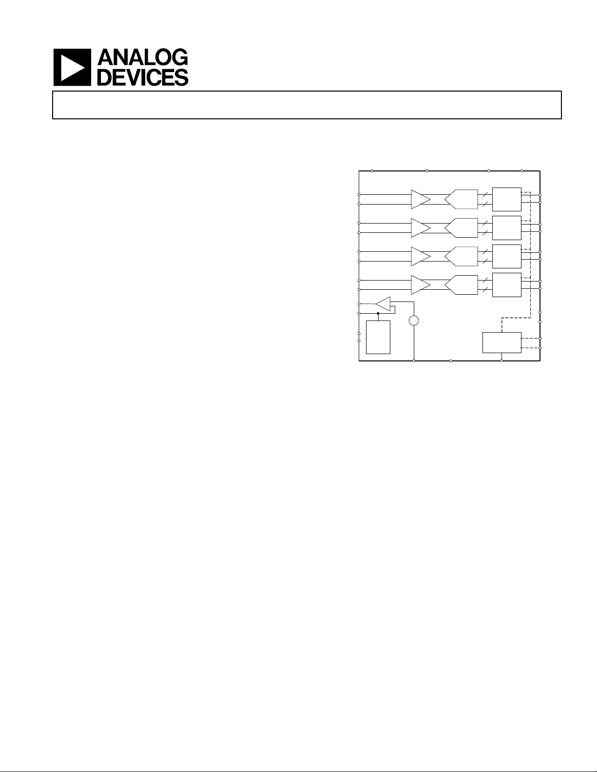
FUNCTIONAL BLOCK DIAGRAM
AVDD
VIN+A
VIN-A
VIN+B
VIN-B
VIN+C
VIN-C
VIN+D
VIN-D
VREF
SENSE
REFT
REFB
Ref
Select
Figure 1. Functional Block Diagram
signal a new output byte. Power down is supported and consumes
less than 3mW when enabled.
PDWN
AD9229
SHA
SHA
SHA
SHA
+
0.5 V
-
AGND
Pipeline
ADC
Pipeline
ADC
Pipeline
ADC
Pipeline
ADC
LVDSBIAS
DRVDD
12
12
12
12
Data Rate
Multiplier
Serial
LVDS
Serial
LVDS
Serial
LVDS
Serial
LVDS
CLK
DRGND
D1+A
D1-A
D1+B
D1-B
D1+C
D1-C
D1+D
D1-D
FCO+
FCO-
DCO+
DCO+
DCO-
DCO-
The AD9229 is a quad 12-bit monolithic sampling analog–to–
digital converter with an on–chip track–and–hold circuit and is
designed for low cost, low power, small size and ease of use. The
product operates up to a 65 MSPS conversion rate and is optimized
for outstanding dynamic performance where a small package size is
critical.
The ADC requires a single+3.0 V power supply and a TTL/CMOS
compatible sample rate clock for full performance operation. No
external reference or driver components are required for many
applications. A separate output power supply pin supports LVDS
compatible serial digital output levels.
The ADC automatically multiplies up the sample rate clock for the
appropriate LVDS serial data rate. An MSB trigger is provided to
Information furnished by Analog Devices is believed to be accurate and reliable.
However, no responsibility is assumed by Analog Devices for its use, nor for any
infringements of patents or other rights of third parties that may result from its
use. No license is granted by implication or otherwise under any patent or patent
rights of Analog Devices. Trademarks and registered trademarks are the property
of their respective companies.
Fabricated on an advanced CMOS process, the AD9229 is available
in a 48-LFCSP package specified over the industrial temperature
range (–40°C to +85°C).
PRODUCT HIGHLIGHTS
1. Four analog-to-digital converters are contained in one small,
space saving package.
2. A Data Clock Output (DCO) is provided which operates up to
390 MHz.
3. The outputs of each ADC are serialized with a maximum data
output rate of 780 Mbps (12-bits x 65 MSPS).
4. The AD9229 operates from a single +3.0 V analog power
supply.
One Technology Way, P.O. Box 9106, Norwood, MA 02062-9106, U.S.A.
Tel: 781.329.4700 www.analog.com
Fax: 781.326.8703 © 2003 Analog Devices, Inc. All rights reserved.

AD9229 Preliminary Technical Data
TABLE OF CONTENTS
AD9229—Specifications ........................................................................3
DIGITAL SPECIFICATIONS...........................................................4
AC SPECIFICATIONS.......................................................................4
SWITCHING SPECIFICATIONS....................................................5
EXPLANATION OF TEST LEVELS................................................5
Absolute Maximum Ratings..................................................................6
EQuivalent circuits..................................................................................7
TYPICAL PERFORMANCE CHARACTERISTICS.........................8
Theory of Operation.............................................................................11
REVISION HISTORY
Revision PrA: Initial Version
Analog Inputs....................................................................................11
Voltage Reference..............................................................................11
Digital Outputs..................................................................................11
Timing ................................................................................................11
PLL......................................................................................................11
Pin Function Descriptions ...................................................................12
Pin Configurations................................................................................13
Timing Diagram....................................................................................14
Ordering Guide.................................................................................15
Revision PrB: Added Definition and Theory of Operation sections, updated Pin Configurations
Revision PrC: Deleted demux outputs
Revision PrD: Added Pin Info, Package Info
Revision PrE: Ch. 3.3V to 3.0V for supply, Updated Sinad spec typo, Added analog typical Cin, Overange Recovery Time, Latency
Revision PrF: Added 50MSPS Grade, Removed Clk-, Updated Power, SNR,LVDS Rset, Tpd Estimates, Added Equiv Ckts, Added FFT, VREF
figure, Corrected FCO, DCO polarity timing
Rev. PrF | Page 2 of 15 Oct. 6, 2003

Preliminary Technical Data AD9229
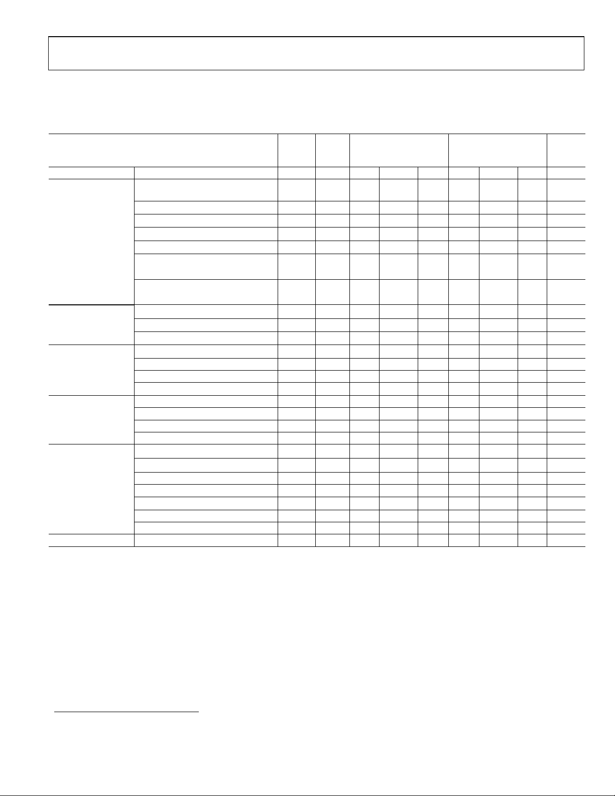
AD9229—SPECIFICATIONS1
AVDD = 3.0V, DRVDD = 3.0V; INTERNAL REFERENCE; DIFFERENTIAL ANALOG INPUTS,MAXIMUM SAMPLE RATE,T
T
, UNLESS OTHERWISE NOTED
MAX
Parameter
Temp Test
Level
AD9229BCP-50
Min Typ Max
AD9229BCP-65
Min Typ Max
MIN
TO
Unit
RESOLUTION 12 12 Bits
ACCURACY
No Missing Codes Full VI Guaran
teed
Offset Error
Gain Error
Offset Matching
Gain Matching2
Differential Nonlinearity (DNL)
25°C
25°C
25°C
25°C
25°C
I
I
± 0.5
± 0.5
I mV
I % FS
I
± 0.3
Guaran
teed
± 0.5
± 0.5
± 0.3
mV
%FS
LSB
Full VI LSB
Integral Nonlinearity (INL)
25°C
I
± 0.6
± 0.6
LSB
Full VI LSB
TEMPERATURE
DRIFT
REFERENCE
Offset Error Full V
Gain Error2 Full V
Reference Full V
Internal Reference Voltage
25°C
I 0.5 0.5 V
Output Current Full V uA
Input Current Full V uA
Input Resistance Full V
ppm/°C
ppm/°C
ppm/°C
kΩ
Differential Input Voltage Range 1 –2 1 –2 Vpp
ANALOG INPUTS
Common Mode Voltage Full V 1.5 1.5 V
Input Capacitance Full V 7 7 pF
Analog Bandwidth, Full Power Full V 500 500 MHz
AVDD Full IV 2.7
DRVDD Full IV 2.7
3.0
3.0
3.6 2.7
3.6 2.7
3.0
3.0
3.6 V
3.6 V
Power Dissipation3 Full VI 940 1250 mW
POWER SUPPLY
Power Down Dissipation Full VI <3 <3 mW
Power Supply Rejection Ratio (PSRR)
25°C
I mV/V
IAVDD3 Full VI 268 367 mA
IDRVDD3 Full VI 28 30 mA
IPLLVDD3 Full VI 18 19
Table 1: DC Specifications
1
Specifications subject to change without notice
2
Gain error and gain temperature coefficients are based on the ADC only (with a fixed 0.5 V external reference and a 1 V p-p differential analog input).
3
Power dissipation measured with rated encode and a dc analog input (Outputs Static, I
Rev. PrF | Page 3 of 15 Oct. 6, 2003
VDD
= 0.). I
VCC
and I
measured with TBD MHz analog input @ 0.5dBFS.
VDD

AD9229 Preliminary Technical Data
DIGITAL SPECIFICATIONS
AVDD = 3.0V, DRVDD = 3.0V
Parameter
VIH Full IV 2.0 2.0 V
CLOCK INPUT
PDWN INPUT
DIGITAL OUTPUTS
(LVDS Mode)*
*
LVDS Rset resistor = 3.6K, LVDS Output Termination Resistor= 100 Ohms.
VIL Full IV 0.8 0.8 V
Input Capacitance
Logic ‘1’ Voltage Full IV 2.0 2.0 V
Logic ‘0’ Voltage Full IV 0.8 0.8 V
Input Capacitance Full IV 2 2 PF
Differential Output Voltage
(VOD)
Output Offset Voltage (VOS) Full IV 1.125 1.375 1.125 1.375 V
Output Coding Full IV Offset Binary Offset Binary
Temp Test
25°C
Full IV 247 454 247 454 mV
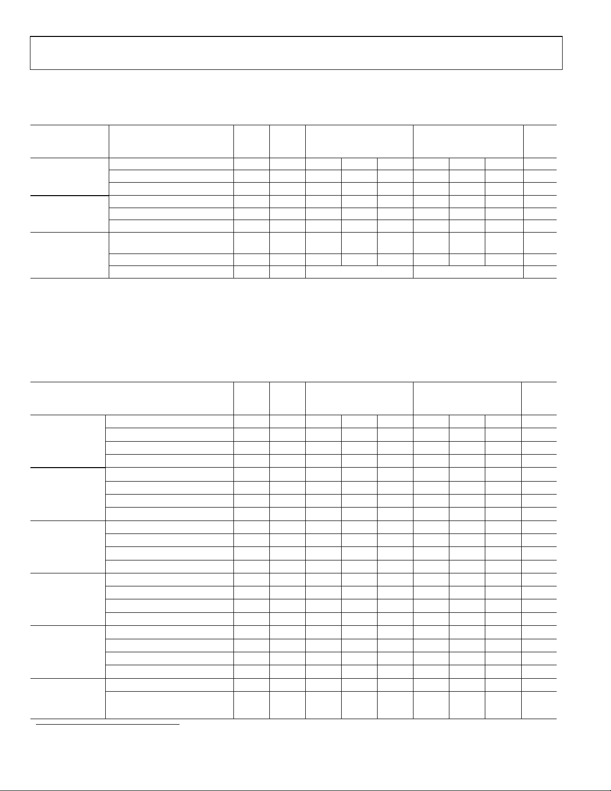
Table 2: Digital Specifications
AC SPECIFICATIONS1
AD9229BCP-50
Level
IV 2 2 pF
Min Typ Max
AD9229BCP-65
Min Typ Max
Unit
AVDD = 3.0 V, DRVDD = 3.0V; INTERNAL REFERENCE; DIFFERENTIAL ANALOG INPUTS,MAXIMUM SAMPLE RATE,T
T
, UNLESS OTHERWISE NOTED
MAX
Parameter Temp Test
Level
SIGNAL TO NOISE
RATIO (SNR) –
Without
Harmonics
SIGNAL TO NOISE
RATIO (SINAD) –
With Harmonics
EFFECTIVE
NUMBER OF BITS
(ENOB)
SPURIOUS FREE
DYNAMIC RANGE
(SFDR)
SECOND AND
THIRD
HARMONIC
DISTORTION
INTERMOD
DISTORTION
(IMD)
1
SNR/harmonics based on an analog input voltage of –0.5 dBFS referenced to a 1 Vpp full-scale input range.
fIN= 10.3 MHz
fIN= 19.6 MHz
fIN= 32.5 MHz
fIN= 51 MHz
fIN= 10.3 MHz
fIN= 19.6 MHz
fIN= 32.5 MHz
fIN= 51 MHz
fIN= 10.3 MHz
fIN= 19.6 MHz
fIN= 32.5 MHz
fIN= 51 MHz
fIN= 10.3 MHz
fIN= 19.6 MHz
fIN= 32.5 MHz
fIN= 51 MHz
fIN= 10.3 MHz
fIN= 19.6 MHz
fIN= 32.5 MHz
fIN= 51 MHz
f
= 19 MHz, f
IN1
f
= xx MHz, f
IN1
= 20 MHz
IN2
= xx MHz
IN2
25°C
25°C
25°C
25°C
25°C
25°C
25°C
25°C
25°C
25°C
25°C
25°C
25°C
25°C
25°C
25°C
25°C
25°C
25°C
25°C
25°C
25°C
V 70.5 70.5 dB
V dB
I 69.7 69.7 dB
V dB
V 70.3 70.3 dB
V dB
I 69.5 69.5 dB
V dB
V Bits
V Bits
I Bits
V Bits
V dB
V 85 85 dB
I dB
V dB
V dBc
V -85 -85 dBc
I dBc
V dBc
V -85 -85 dBc TWO TONE
V dBc
AD9229BCP-50
Min Typ Max
AD9229BCP-65
Min Typ Max
TO
MIN
Unit
Rev. PrF | Page 4 of 15 Oct. 6, 2003

Preliminary Technical Data AD9229
Parameter Temp Test
Level
CROSSTALK Full V -80 -80 dB
Table 3: AC Specifications
SWITCHING SPECIFICATIONS
AVDD = 3.0 V, DRVDD = 3.0 V; DIFFERENTIAL ENCODE INPUT
AD9229BCP-50
Min Typ Max
AD9229BCP-65
Min Typ Max
Unit
Parameter Temp Test
Clock Rate Full VI 10 50 10 65 MSPS
CLOCK
OUTPUT
PARAMETERS IN
LVDS MODE
APERTURE
Out of Range
Recovery Time
Clock Pulse Width High (tEH) Full IV ns
Clock Pulse Width Low (tEL) Full IV ns
Valid Time (tV)1 Full VI ns
Propagation Delay (tPD) 1 Full VI 5 5 ns
MSB Propagation Delay (t
Rise Time (tR) (20% to 80%) Full V ns
Fall Time (tF) (20% to 80%) Full V ns
DCO Propagation Delay (t
Data to DCO Skew (tPD – t
Pipeline Latency Full VI 9 9 cycles
Aperture Delay (tA)
Aperture Uncertainty (Jitter)
Full IV 2 2 cycles
) 1 Full VI 5 5 ns
MSB
) Full VI 5 5 ns
CPD
) Full IV ns
CPD
EXPLANATION OF TEST LEVELS
TEST LEVEL
I 100% production tested.
AD9229BCP-50
Level
25°C
25°C
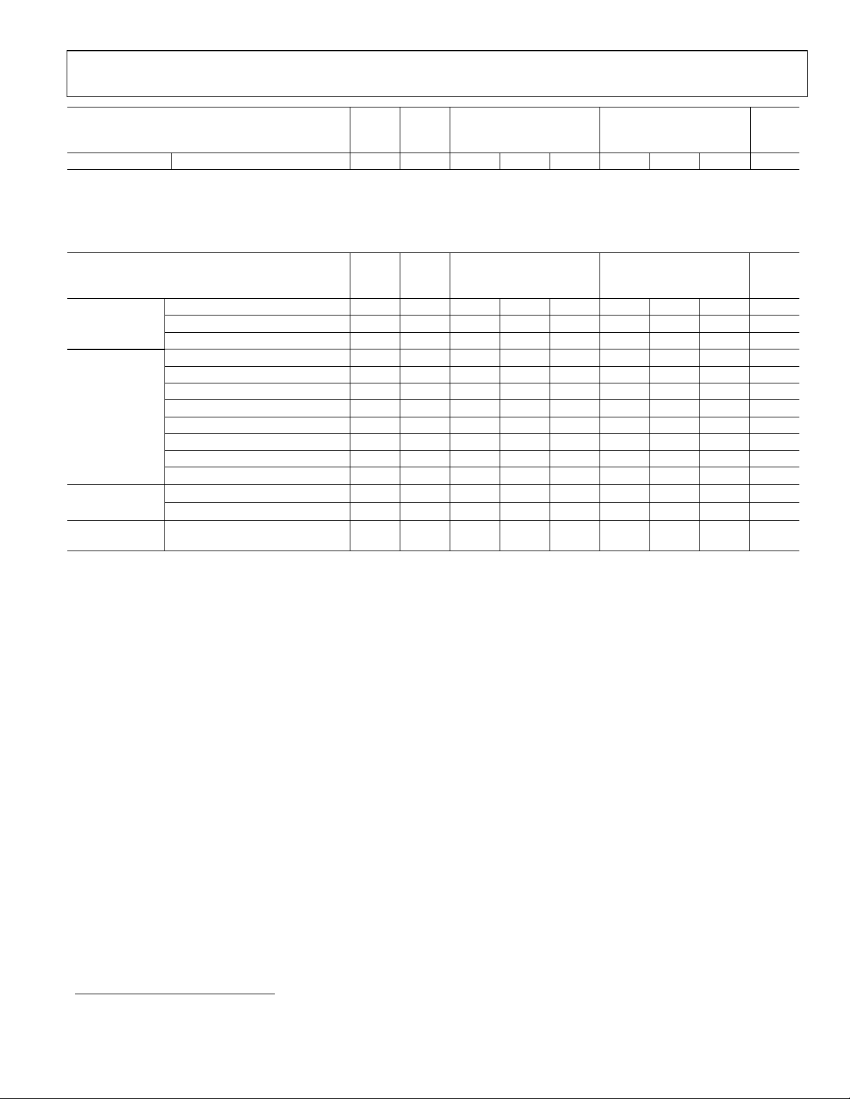
Table 4: Switching Specifications
V ps
V <1 <1 ps rms
Min Typ Max
AD9229BCP-65
Min Typ Max
Unit
II 100% production tested at +25°C and guaranteed by design and characterization at specified temperatures.
III Sample tested only.
IV Parameter is guaranteed by design and characterization testing.
V Parameter is a typical value only.
VI 100% production tested at +25°C and guaranteed by design and characterization for industrial temperature range.
1
t
and t
are measured from the transition points of the CLK input to the 50%/50% levels of the digital outputs swing. The digital output load during test is
V
PD
not to exceed an ac load of 5 pF or a dc current of ±40 µA. Rise and fall times measured from 20% to 80%.
Rev. PrF | Page 5 of 15 Oct. 6, 2003
 Loading...