

Page 1
Quad, 12-Bit, 50/65 MSPS,
FEATURES
Four ADCs in 1 package
Serial LVDS digital output data rates
to 780 Mbps (ANSI-644)
Data and frame clock outputs
SNR = 69.5 dB (to Nyquist)
Excellent linearity
DNL = ±0.3 LSB (typical)
INL = ±0.4 LSB (typical)
400 MHz full power analog bandwidth
Power dissipation
1,350 mW at 65 MSPS
985 mW at 50 MSPS
1 V p-p to 2 V p-p input voltage range
3.0 V supply operation
Power-down mode
Digital test pattern enable for timing alignments
APPLICATIONS
Digital beam-forming systems for ultrasound
Wireless and wired broadband communications
Communication test equipment
GENERAL DESCRIPTION
Serial, LVDS, 3 V A/D Converter
AD9229
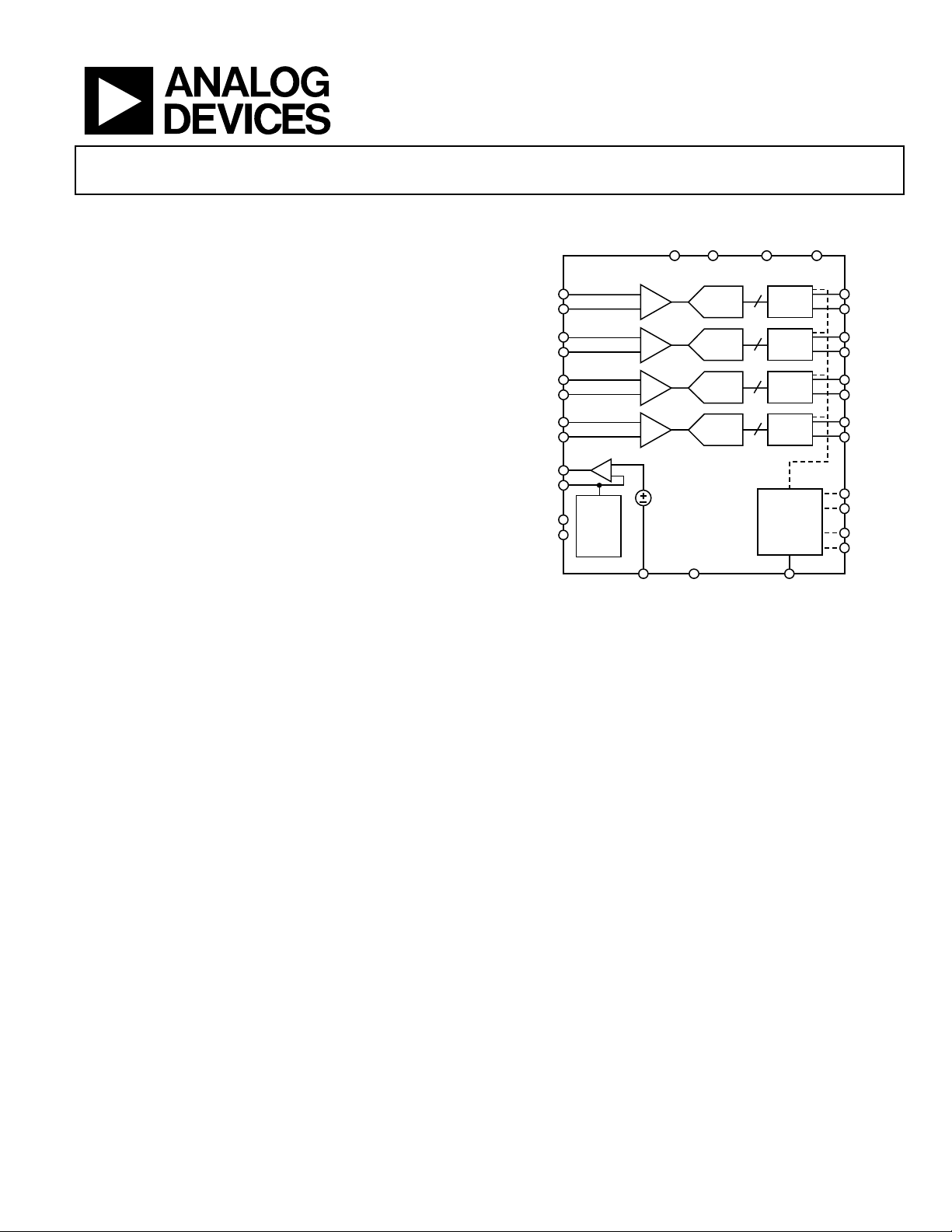
FUNCTIONAL BLOCK DIAGRAM
PDWN DTP DRVDD DRGND
AD9229
VIN+A
VIN–A
VIN+B
VIN–B
VIN+C
VIN–C
VIN+D
VIN–D
VREF
SENSE
REFT
REFB
REF
SELECT
SHA
SHA
SHA
SHA
0.5V
AGND CLKLVDSBIAS
PRODUCT HIGHLIGHTS
PIPELINE
PIPELINE
PIPELINE
PIPELINE
Figure 1.
ADC
ADC
ADC
ADC
12
SERIAL
12
SERIAL
12
SERIAL
12
SERIAL
DATA RATE
MULTIPLIER
LVDS
LVDS
LVDS
LVDS
D+A
D–A
D+B
D–B
D+C
D–C
D+D
D–D
FCO+
FCO–
DCO+
DCO–
04418-001
The AD9229 is a quad, 12-bit, 65 MSPS analog-to-digital
converter (ADC) with an on-chip sample-and-hold circuit that
is designed for low cost, low power, small size, and ease of use.
The product operates at up to a 65 MSPS conversion rate and is
optimized for outstanding dynamic performance in applications
where a small package size is critical.
The ADC requires a single 3 V power supply and TTL-/CMOScompatible sample rate clock for full performance operation.
No external reference or driver components are required for
many applications.
The ADC automatically multiplies the sample rate clock for the
appropriate LVDS serial data rate. A data clock (DCO) for
capturing data on the output and a frame clock (FCO) trigger
for signaling a new output byte are provided. Power-down is
supported and typically consumes 3 mW when enabled.
Fabricated with an advanced CMOS process, the AD9229 is
available in a Pb-free, 48-lead LFCSP package. It is specified
over the industrial temperature range of –40°C to +85°C.
Rev. A
Information furnished by Analog Devices is believed to be accurate and reliable. However, no
responsibility is assumed by Anal og Devices for its use, nor for any infringements of patents or ot her
rights of third parties that may result from its use. Specifications subject to change without notice. No
license is granted by implication or otherwise under any patent or patent rights of Analog Devices.
Trademarks and registered trademarks are the property of their respective owners.
1. Four ADCs are contained in a small, space-saving package.
2. A data clock out (DCO) is provided, which operates up to
390 MHz and supports double-data rate operation (DDR).
3. The outputs of each ADC are serialized LVDS with data
rates up to 780 Mbps (12 bits × 65 MSPS).
4. The AD9229 operates from a single 3.0 V power supply.
5. Packaged in a Pb-free, 48-lead LFCSP package.
6. The internal clock duty cycle stabilizer maintains
performance over a wide range of input clock duty cycles.
One Technology Way, P.O. Box 9106, Norwood, MA 02062-9106, U.S.A.
Tel: 781.329.4700 www.analog.com
Fax: 781.461.3113 © 2005 Analog Devices, Inc. All rights reserved.
Page 2

AD9229
TABLE OF CONTENTS
Features.............................................................................................. 1
Applications....................................................................................... 1
Functional Block Diagram .............................................................. 1
General Description ......................................................................... 1
Revision History ............................................................................... 2
Specifications..................................................................................... 3
AC Specifications.......................................................................... 4
Digital Specifications ................................................................... 5
Switching Specifications.............................................................. 6
Timing Diagram ............................................................................... 7
Absolute Maximum Ratings............................................................ 8
Explanation of Test Levels........................................................... 8
ESD Caution.................................................................................. 8
Pin Configuration and Function Descriptions............................. 9
Equivalent Circuits......................................................................... 10
Typical Performance Characteristics........................................... 11
Terminology.................................................................................... 16
Theory of Operation ...................................................................... 18
Analog Input Considerations ................................................... 18
Clock Input Considerations...................................................... 19
Evaluation Board............................................................................ 24
Power Supplies............................................................................ 24
Input Signals................................................................................ 24
Output Signals ............................................................................ 24
Default Operation and Jumper Selection Settings ................. 25
Alternate Analog Input Drive Configuration......................... 25
Outline Dimensions....................................................................... 39
Ordering Guide .......................................................................... 39
REVISION HISTORY
9/05—Rev. 0 to Rev. A
Change to Specifications.................................................................. 3
Changes to Differential Input Configurations Section.............. 19
Changes to Exposed Paddle Thermal Heat Slug
Recommendations Section........................................................ 23
Changes to Evaluation Board Section.......................................... 24
Changes to Table 11........................................................................ 36
3/05—Revision 0: Initial Version
Rev. A | Page 2 of 40
Page 3

AD9229
SPECIFICATIONS
AVDD = 3.0 V, DRVDD = 3.0 V, maximum conversion rate, 2 V p-p differential input, 1.0 V internal reference, AIN = –0.5 dBFS, unless
otherwise noted.
Table 1.
AD9229-50 AD9229-65
Te st
Parameter Temperature
RESOLUTION 12 12 Bits
ACCURACY
No Missing Codes Full VI Guaranteed Guaranteed
Offset Error Full VI ±5 ±25 ±5 ±25 mV
Offset Matching Full VI ±5 ±25 ±5 ±25 mV
Gain Error1 Full VI ±0.3 ±2.5 ±0.3 ±2.5 % FS
Gain Matching1 Full VI ±0.2 ±1.5 ±0.2 ±1.5 % FS
Differential Nonlinearity (DNL) 25°C V ±0.3 ±0.3 LSB
Full VI ±0.3 ±0.6 ±0.3 ±0.7 LSB
Integral Nonlinearity (INL) 25°C V ±0.6 ±0.4 LSB
Full VI ±0.6 ±1 ±0.4 ±1 LSB
TEMPERATURE DRIFT
Offset Error Full V ±2 ±3 ppm/°C
Gain Error1 Full V ±12 ±12 ppm/°C
Reference Voltage, VREF = 1 V Full V ±16 ±16 ppm/°C
REFERENCE
Output Voltage Error, VREF = 1 V Full VI ±10 ±30 ±10 ±30 mV
Load Regulation @ 1.0 mA, VREF = 1 V Full V 3 3 mV
Output Voltage Error, VREF = 0.5 V Full VI ±8 ±17 ±8 ±17 mV
Load Regulation @ 0.5 mA,
Full V 0.2 0.2 mV
VREF = 0.5 V
Input Resistance Full V 7 7 kΩ
ANALOG INPUTS
Differential Input Voltage Range
Full VI 2 2 V p-p
VREF = 1 V
Differential Input Voltage Range
Full VI 1 1 V p-p
VREF = 0.5 V
Common Mode Voltage Full V 1.5 1.5 V
Input Capacitance2 Full V 7 7 pF
Analog Bandwidth, Full Power Full V 400 400 MHz
POWER SUPPLY
AVDD Full IV 2.7 3.0 3.6 2.7 3.0 3.6 V
DRVDD Full IV 2.7 3.0 3.6 2.7 3.0 3.6 V
IAVDD Full VI 300 330 420 455 mA
DRVDD Full VI 28 31 29 33 mA
Power Dissipation3 Full VI 985 1083 1350 1465 mW
Power-Down Dissipation Full V 3 3 mW
CROSSTALK4 Full V –95 –95 dB
1
Gain error and gain temperature coefficients are based on the ADC only, with a fixed 1.0 V external reference and a 2 V p-p differential analog input.
2
Input capacitance refers to the effective capacitance between one differential input pin and AGND. Refer to Figure 4 for the equivalent analog input structure.
3
Power dissipation measured with rated encode and 2.4 MHz analog input at –0.5 dBFS.
4
Typical specification over the first Nyquist zone.
Level Min Typ Max Min Typ Max Unit
Rev. A | Page 3 of 40
Page 4

AD9229
AC SPECIFICATIONS
AVDD = 3.0 V, DRVDD = 3.0 V, maximum conversion rate, 2 V p-p differential input, 1.0 V internal reference, AIN = –0.5 dBFS, unless
otherwise noted.
Table 2.
AD9229-50 AD9229-65
Te st
Parameter Temperature
SIGNAL-TO-NOISE RATIO (SNR) fIN = 2.4 MHz Full IV 69.5 70.4 69.0 70.2 dB
f
f
f
f
= 10.3 MHz 25°C V 70.4 70.2 dB
IN
= 25 MHz Full VI 68.7 69.6 dB
IN
= 30 MHz Full VI 68.0 69.5 dB
IN
= 70 MHz 25°C V 67.2 67.1 dB
IN
SIGNAL-TO-NOISE RATIO (SINAD) fIN = 2.4 MHz Full V 70.0 69.8 dB
f
f
f
f
EFFECTIVE NUMBER OF BITS
= 10.3 MHz 25°C V 70.0 69.8 dB
IN
= 25 MHz Full VI 68.4 69.4 dB
IN
= 30 MHz Full VI 67.3 69.0 dB
IN
= 70 MHz 25°C V 66.8 66.7 dB
IN
= 2.4 MHz Full V 11.3 11.3 Bits
f
IN
(ENOB)
f
f
f
f
SPURIOUS-FREE DYNAMIC RANGE
= 10.3 MHz 25°C V 11.3 11.3 Bits
IN
= 25 MHz Full VI 11.1 11.2 Bits
IN
= 30 MHz Full VI 10.9 11.2 Bits
IN
= 70 MHz 25°C V 10.8 10.8 Bits
IN
= 2.4 MHz Full V 85 85 dBc
f
IN
(SFDR)
f
f
f
f
= 10.3 MHz 25°C V 85 85 dBc
IN
= 25 MHz Full VI 76 85 dBc
IN
= 30 MHz Full VI 73 85 dBc
IN
= 70 MHz 25°C V 78 77 dBc
IN
WORST HARMONIC fIN = 2.4 MHz Full V –85 –85 dBc
(Second or Third) fIN = 10.3 MHz 25°C V –85 –85 dBc
f
f
f
= 25 MHz Full VI –85 –76 dBc
IN
= 30 MHz Full VI –85 –73 dBc
IN
= 70 MHz 25°C V –78 –77 dBc
IN
WORST OTHER fIN = 2.4 MHz Full V –90 –90 dBc
(Excluding Second or Third) fIN = 10.3 MHz 25°C V –90 –90 dBc
f
f
f
TWO-TONE INTERMODULATION
= 25 MHz Full VI –88 –81.7 dBc
IN
= 30 MHz Full VI –88 –79.7 dBc
IN
= 70 MHz 25°C V –85 –83 dBc
IN
= 15 MHz 25°C V –73 –73 dBc
f
IN1
DISTORTION (IMD)
AIN1 and AIN2 = –7.0 dBFS f
f
f
= 16 MHz
IN2
= 69 MHz 25°C V –68.5 –68.5 dBc
IN1
= 70 MHz
IN2
Level
Min Typ Max Min Typ Max Unit
Rev. A | Page 4 of 40
Page 5

AD9229
DIGITAL SPECIFICATIONS
AVDD = 3.0 V, DRVDD = 3.0 V, maximum conversion rate, 2 V p-p differential input, 1.0 V internal reference, AIN = –0.5 dBFS, unless
otherwise noted.
Table 3.
AD9229-50 AD9229-65
Te st
Parameter Temperature
CLOCK INPUT
Logic Compliance TTL/CMOS TTL/CMOS
High Level Input Voltage Full IV 2.0 2.0 V
Low Level Input Voltage Full IV 0.8 0.8 V
High Level Input Current Full VI 0.5 ±10 0.5 ±10 µA
Low Level Input Current Full VI 0.5 ±10 0.5 ±10 µA
Input Capacitance 25°C V 2 2 pF
LOGIC INPUTS (PDWN)
Logic 1 Voltage Full IV 2.0 2.0 V
Logic 0 Voltage Full IV 0.8 0.8 V
High Level Input Current Full IV 0.5 ±10 0.5 ±10 µA
Low Level Input Current Full IV 0.5 ±10 0.5 ±10 µA
Input Capacitance 25°C V 2 2 pF
DIGITAL OUTPUTS (D+, D–)
Logic Com plian ce LVDS LVDS
Differential Output Voltage Full VI 260 440 260 440 mV
Output Offset Voltage Full VI 1.15 1.25 1.35 1.15 1.25 1.35 V
Output Coding Full VI
Level
Min Typ Max Min Typ Max Unit
Offset
binary
Offset
binary
Rev. A | Page 5 of 40
Page 6

AD9229
SWITCHING SPECIFICATIONS
AVDD = 3.0 V, DRVDD = 3.0 V, maximum conversion rate, 2 V p-p differential input, 1.0 V internal reference, AIN = –0.5 dBFS, unless
otherwise noted.
Table 4.
AD9229-50 AD9229-65
Test
Parameter Temp
CLOCK
Maximum Clock Rate Full VI 50 65 MSPS
Minimum Clock Rate Full IV 10 10 MSPS
Clock Pulse Width High
)
(t
EH
Clock Pulse Width Low
(t
)
EL
Full VI 8 10 6.2 7.7 ns
Full VI 8 10 6.2 7.7 ns
OUTPUT PARAMETERS
Propagation Delay (tPD) Full VI 3.3 6.5 7.9 3.3 6.5 7.9 ns
Rise Time (tR)
Full V 250 250 ps
(20% to 80%)
Fall Time (tF)
Full V 250 250 ps
(20% to 80%)
FCO Propagation Delay
)
(t
FCO
DCO Propagation Delay
)
(t
CPD
DCO-to-Data Delay (t
DCO-to-FCO Delay (t
Data-to-Data Skew
– t
(t
DATA-MAX
DATA-MIN
Full V 6.5 6.5 ns
Full V t
) Full IV (t
DATA
) Full IV (t
FRAME
Full IV ±100 ±250 ±100 ±250 ps
)
Wake-Up Time 25°C V 4 4 ms
Pipeline Latency Full IV 10 10 CLK
APERTURE
Aperture Delay (tA) 25°C V 1.8 1.8 ns
Aperture Uncertainty
25°C V <1 <1 ps
(Jitter)
OUT-OF-RANGE RECOVERY
25°C V 2 2 CLK
TIME
Level
Min Typ Max Min Typ Max Unit
SAMPLE
250
SAMPLE
250
/24) –
/24) –
FCO
(t
(t
(t
SAMPLE
SAMPLE
SAMPLE
+
/24)
/24) (t
/24) (t
t
SAMPLE
250
SAMPLE
250
/24) +
/24) +
(t
SAMPLE
250
(t
SAMPLE
250
/24) –
/24) –
FCO
(t
(t
(t
SAMPLE
SAMPLE
SAMPLE
+
/24)
/24) (t
/24) (t
ns
SAMPLE
/24) +
ps
250
SAMPLE
/24) +
ps
250
cycles
rms
cycles
Rev. A | Page 6 of 40
Page 7
AD9229
TIMING DIAGRAM
N–1
AIN
t
A
CLK
DCO–
DCO+
FCO–
FCO+
D+
t
EH
t
CPD
t
FCO
t
D–
PD
t
FRAME
MSB
D10
(N – 10)
(N–10)D9(N–10)D8(N – 10)D7(N – 10)D6(N – 10)D5(N – 10)D4(N–10)D3(N – 10)D2(N – 10)D1(N – 10)D0(N–10)
t
EL
t
DATA
Figure 2. Timing Diagram
N
D10
MSB
(N – 9)
(N – 9)
04418-002
Rev. A | Page 7 of 40
Page 8
AD9229
ABSOLUTE MAXIMUM RATINGS
Table 5.
With
Parameter
ELECTRICAL
AVDD AGND –0.3 V to +3.9 V
DRVDD DRGND –0.3 V to +3.9 V
AGND DRGND –0.3 V to +0.3 V
AVDD DRVDD –3.9 V to +3.9 V
Digital Outputs (D+, D–,
DCO+, DCO–, FCO+, FCO–)
LVDSBIAS DRGND –0.3 V to DRVDD
CLK AGND –0.3 V to AVDD
VIN+, VIN– AGND –0.3 V to AVDD
PDWN, DTP AGND –0.3 V to AVDD
REFT, REFB AGND –0.3 V to AVDD
VREF, SENSE AGND –0.3 V to AVDD
ENVIRONMENTAL
Operating Temperature
Range (Ambient)
Maximum Junction
Temperature
Lead Temperature
(Soldering, 10 sec)
Storage Temperature Range
(Ambient)
Thermal Impedance1 25°C/W
Respect To
DRGND –0.3 V to DRVDD
–40°C to +85°C
150°C
300°C
–65°C to +150°C
Rating
Stresses above those listed under Absolute Maximum Ratings
may cause permanent damage to the device. This is a stress
rating only; functional operation of the device at these or any
other conditions above those indicated in the operational
section of this specification is not implied. Exposure to absolute
maximum rating conditions for extended periods may affect
device reliability.
EXPLANATION OF TEST LEVELS
I. 100% production tested.
II. 100% production tested at 25°C and guaranteed by design
and characterization at specified temperatures.
III. Sample tested only.
IV. Parameter is guaranteed by design and characterization
testing.
V. Parameter is a typical value only.
VI. 100% production tested at 25°C and guaranteed by design
and characterization for industrial temperature range.
1
θ
for a 4-layer PCB with a solid ground plane in still air.
JA
ESD CAUTION
ESD (electrostatic discharge) sensitive device. Electrostatic charges as high as 4000 V readily accumulate on
the human body and test equipment and can discharge without detection. Although this product features
proprietary ESD protection circuitry, permanent damage may occur on devices subjected to high energy
electrostatic discharges. Therefore, proper ESD precautions are recommended to avoid performance
degradation or loss of functionality.
Rev. A | Page 8 of 40
Page 9
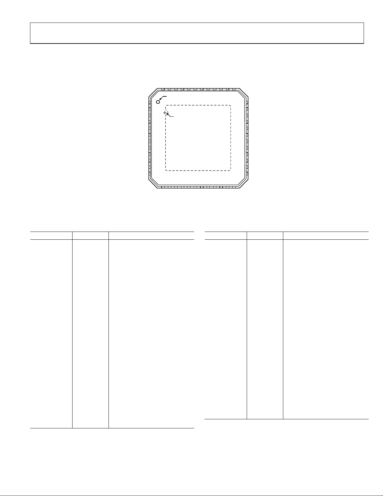
AD9229
PIN CONFIGURATION AND FUNCTION DESCRIPTIONS
DCO+
DCO–
FCO+
FCO–
D+A
D–A
D+B
D–B
D+C
D–C
D+D
D–D
DRGND
DRVDD
NC
DTP
AVDD
AGND
PDWN
AVDD
AGND
VIN+A
VIN–A
AGND
4847464544434241403938
PIN 1
1
2
3
4
5
6
7
8
9
10
11
12
INDICATOR
EXPOSED PADDLE, PIN 0
(Bottom of Package)
AD9229
TOP VIEW
(Not to Scale)
37
DRGND36
DRVDD
35
LVDSBIAS
34
AGND
33
AVDD
32
AGND
31
CLK
30
AVDD
29
AGND
28
VIN+D
27
VIN–D
26
AGND
25
NC = NO CONNECT
13141516171819
VIN–B
AGND
VIN+B
Figure 3. LFCSP Top View
Table 6. Pin Function Descriptions
Pin No. Mnemonic Description
5, 8, 16, 21,
AVDD Analog Supply
29, 32
6, 9, 12, 15, 22,
AGND Analog Ground
25, 28, 31, 33
2, 35 DRVDD Digital Output Supply
1, 36 DRGND Digital Ground
0 AGND
Exposed Paddle/Thermal Heat
Slug (Located on Bottom of
Package)
3 NC No Connect
4 DTP Digital Test Pattern Enable
7 PDWN
Power-Down Selection (AVDD =
Power Down)
10 VIN+A ADC A Analog Input—True
11 VIN–A
ADC A Analog Input—
Complement
13 VIN–B
ADC B Analog Input—
Complement
14 VIN+B ADC B Analog Input—True
17 SENSE Reference Mode Selection
18 VREF Voltage Reference Input/Output
19 REFB Differential Reference (Bottom)
20 REFT Differential Reference (Top)
23 VIN+C ADC C Analog Input—True
24 VIN–C
ADC C Analog Input—
Complement
AVDD
SENSE
2021222324
REFT
VREF
REFB
AVDD
AGND
VIN–C
VIN+C
04418-003
Pin No. Mnemonic Description
26 VIN–D
ADC D Analog Input—
Complement
27 VIN+D ADC D Analog Input—True
30 CLK Input Clock
34 LVDSBIAS
LVDS Output Current Set
Resistor Pin
37 D–D
ADC D Complement Digital
Output
38 D+D ADC D True Digital Output
39 D–C
ADC C Complement Digital
Output
40 D+C ADC C True Digital Output
41 D–B
ADC B Complement Digital
Output
42 D+B ADC B True Digital Output
43 D–A
ADC A Complement Digital
Output
44 D+A ADC A True Digital Output
45 FCO–
Frame Clock Indicator—
Complement Output
46 FCO+
Frame Clock Indicator—True
Output
47 DCO–
Data Clock Output—
Complement
48 DCO+ Data Clock Output—True
Rev. A | Page 9 of 40
Page 10
AD9229
CLK
EQUIVALENT CIRCUITS
AVDD
DRVDD
VIN+, VIN–
AGND
04418-004
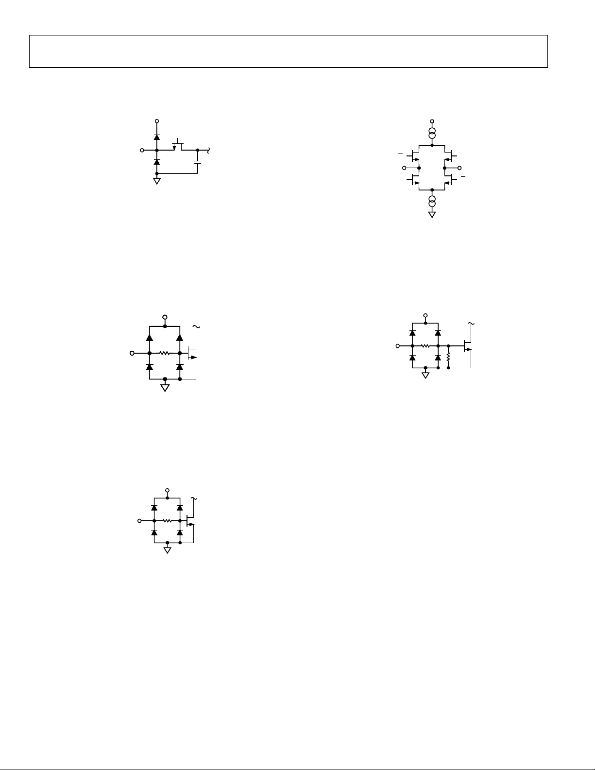
Figure 4. Equivalent Analog Input Circuit
AVDD
170Ω
AGND
04418-005
V
D– D+
V
DRGND
V
V
04418-007
Figure 7. Equivalent Digital Output Circuit
AVDD
DTP
375Ω
AGND
100kΩ
04418-051
Figure 5. Equivalent Clock Input Circuit
AVDD
PDWN
375Ω
AGND
04418-006
Figure 8. Equivalent DTP Input Circuit
Figure 6. Equivalent Digital Input Circuit
Rev. A | Page 10 of 40
Page 11
AD9229
TYPICAL PERFORMANCE CHARACTERISTICS
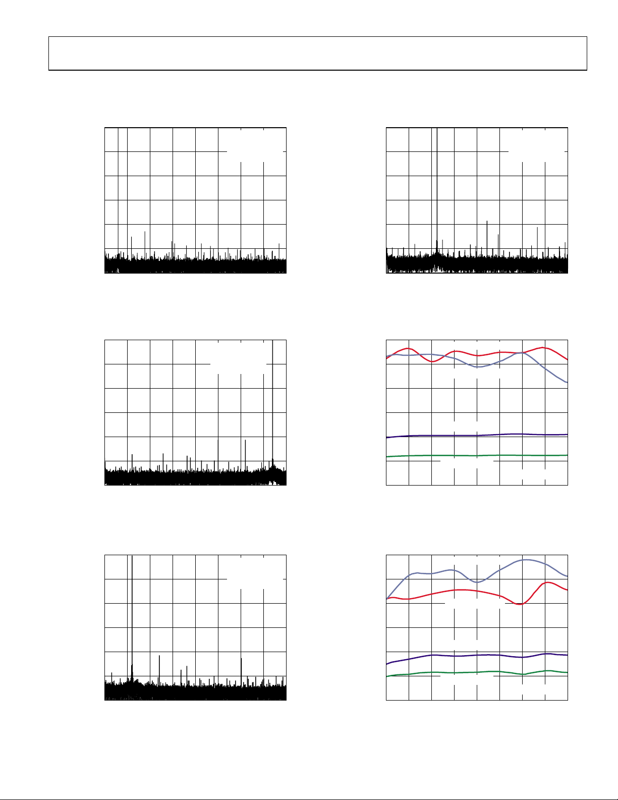
–20
0
AIN = –0.5dBFS
SNR = 70.4dB
ENOB = 11.4 BITS
SFDR = 85.8dBC
–20
0
AIN = –0.5dBFS
SNR = 68.1dB
ENOB = 11.0 BITS
SFDR = 77.0dBC
–40
–60
–80
AMPLITUDE (dBFS)
–100
–120
0 8.14.1 12.2 16.3 20.3 24.4 28.4 32.5
Figure 9. Single-Tone 32k FFT with f
0
–20
–40
–60
–80
AMPLITUDE (dBFS)
–100
–120
0 8.14.1 12.2 16.3 20.3 24.4 28.4 32.5
Figure 10. Single-Tone 32k FFT with f
FREQUENCY (MHz)
= 2.4 MHz, f
IN
AIN = –0.5dBFS
SNR = 69.6dB
ENOB = 11.3 BITS
SFDR = 82.4dBC
FREQUENCY (MHz)
= 30 MHz, f
IN
SAMPLE
SAMPLE
= 65 MSPS
= 65 MSPS
04418-009
04418-010
–40
–60
–80
AMPLITUDE (dBFS)
–100
–120
0 8.14.1 12.2 16.3 20.3 24.4 28.4 32.5
Figure 12. Single-Tone 32k FFT with f
90
85
80
75
SNR/SFDR (dB)
70
65
60
10 2015 25 30 35 40 45 50
Figure 13. SNR/SFDR vs. f
FREQUENCY (MHz)
= 120 MHz, f
IN
1V p-p, SFDR (dBc)
2V p-p, SFDR (dBc)
2V p-p, SNR (dB)
1V p-p, SNR (dB)
ENCODE (MSPS)
, fIN = 10.3 MHz, f
SAMPLE
AIN = –0.5dBFS
SAMPLE
= 65 MSPS
SAMPLE
= 50 MSPS
04418-012
04418-013
0
–20
–40
–60
–80
AMPLITUDE (dBFS)
–100
–120
0 8.14.1 12.2 16.3 20.3 24.4 28.4 32.5
Figure 11. Single-Tone 32k FFT with f
FREQUENCY (MHz)
IN
AIN = –0.5dBFS
SNR = 68.5dB
ENOB = 11.1 BITS
SFDR = 81.3dBC
= 70 MHz, f
SAMPLE
= 65 MSPS
Rev. A | Page 11 of 40
04418-011
90
85
80
75
SNR/SFDR (dB)
70
65
60
10 2015 25 30 35 40 45 50
Figure 14. SNR/SFDR vs. f
1V p-p, SFDR (dBc)
2V p-p, SFDR (dBc)
2V p-p, SNR (dB)
1V p-p, SNR (dB)
ENCODE (MSPS)
, fIN = 25 MHz, f
SAMPLE
AIN = –0.5dBFS
SAMPLE
04418-014
= 50 MSPS
Page 12
AD9229
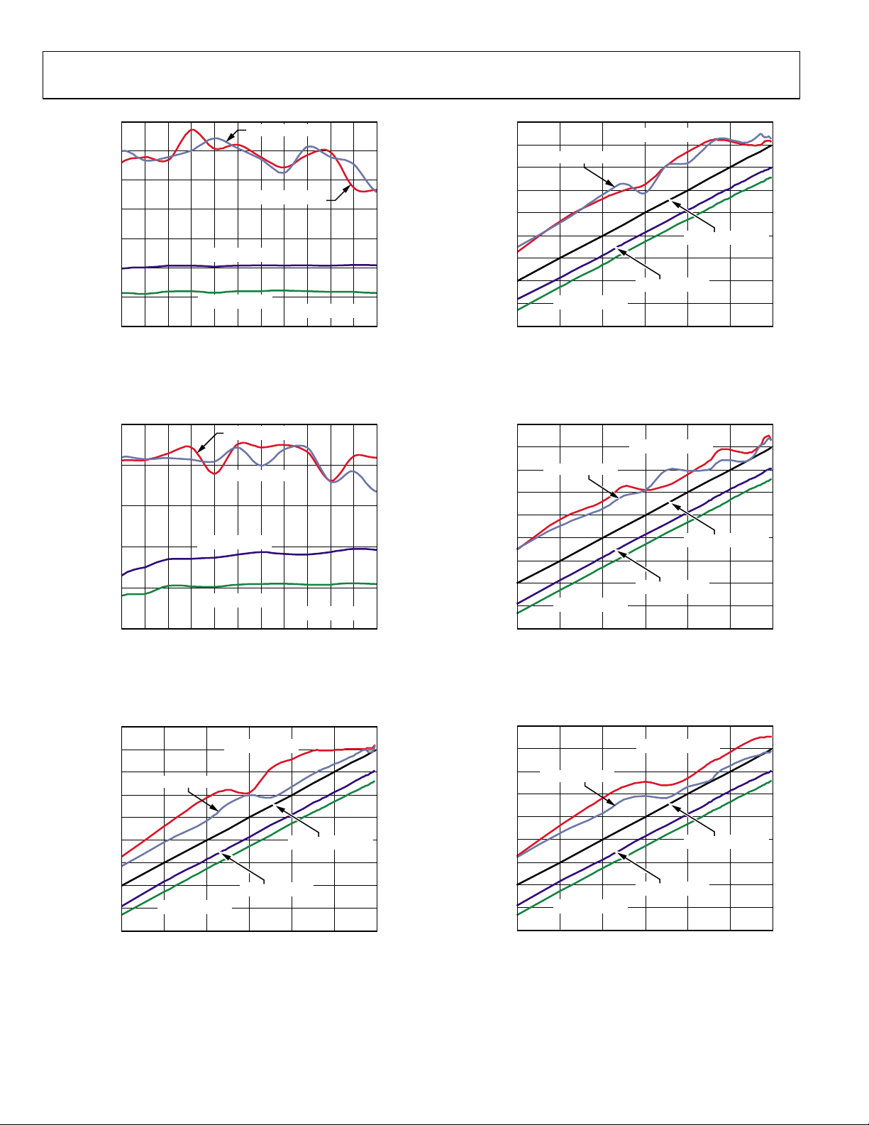
95
90
85
80
75
SNR/SFDR (dB)
70
65
60
Figure 15. SNR/SFDR vs. f
1V p-p, SFDR (dBc)
2V p-p, SFDR (dBc)
2V p-p, SNR (dB)
1V p-p, SNR (dB)
10 2015 25 30 35 40 45 6550 55 60
ENCODE (MSPS)
, fIN = 10.3 MHz, f
SAMPLE
AIN = –0.5dBFS
= 65 MSPS
SAMPLE
04418-015
90
80
1V p-p, SFDR (dBc)
70
60
50
40
SNR/SFDR (dB)
30
20
10
0
–60 –10–20–30–40–50 0
1V p-p, SNR (dB)
2V p-p, SFDR (dBc)
80 dB REFERENCE
2V p-p, SNR (dB)
ANALOG INPUT LEVEL (dBFS)
Figure 18. SNR/SFDR vs. Analog Input Level,
=25 MHz, f
f
IN
SAMPLE
= 50 MSPS
04418-018
85
80
75
70
SNR/SFDR (dB)
65
60
10 2015 25 30 35 40 45 6550 55 60
Figure 16. SNR/SFDR vs. f
90
80
70
1V p-p, SFDR (dBc)
60
50
40
SNR/SFDR (dB)
30
20
10
0
–60 –10–20–30–40–50 0
1V p-p, SNR (dB)
2V p-p, SFDR (dBc)
1V p-p, SFDR (dBc)
2V p-p, SNR (dB)
1V p-p, SNR (dB)
ENCODE (MSPS)
, fIN = 30 MHz, f
SAMPLE
2V p-p, SFDR (dBc)
2V p-p, SNR (dB)
ANALOG INPUT LEVEL (dBFS)
SAMPLE
80 dB REFERENCE
AIN = –0.5dBFS
Figure 17. SNR/SFDR vs. Analog Input Level,
= 10.3 MHz, f
f
IN
SAMPLE
= 50 MSPS
= 65 MSPS
04418-016
04418-017
90
80
1V p-p, SFDR (dBc)
70
60
50
40
SNR/SFDR (dB)
30
20
10
0
–60 –10–20–30–40–50 0
1V p-p, SNR (dB)
ANALOG INPUT LEVEL (dBFS)
2V p-p, SFDR (dBc)
80 dB REFERENCE
2V p-p, SNR (dB)
Figure 19. SNR/SFDR vs. Analog Input Level,
= 10.3 MHz, f
f
IN
90
80
70
1V p-p, SFDR (dBc)
60
50
40
SNR/SFDR (dB)
30
20
10
0
–60 –10–20–30–40–50 0
1V p-p, SNR (dB)
ANALOG INPUT LEVEL (dBFS)
= 65 MSPS
SAMPLE
2V p-p, SFDR (dBc)
80 dB REFERENCE
2V p-p, SNR (dB)
Figure 20. SNR/SFDR vs. Analog Input Level,
= 30 MHz, f
f
IN
SAMPLE
= 65 MSPS
04418-019
04418-020
Rev. A | Page 12 of 40
Page 13

AD9229
90
85
80
75
70
65
SNR/SFDR (dB)
60
55
50
45
1 10010 1000
Figure 21. SNR/SFDR vs. f
SFDR (dBc)
SNR (dB)
FREQUENCY (MHz)
, f
IN
SAMPLE
= 65 MHz
04418-021
80
70
60
50
40
SFDR (dB)
30
20
10
0
–60 –19 –10–28–36–44–52–56 –15–23–32–40–48 –7
Figure 24. Two-Tone SFDR vs. Analog Input Level, f
2V p-p, SFDR (dBc)
1V p-p, SFDR (dBc)
ANALOG INPUT LEVEL (dBFS)
= 16 MHz, f
f
IN2
SAMPLE
= 65 MSPS
80 dB REFERENCE
IN1
= 15 MHz and
04418-024
0
–20
–40
–60
–80
AMPLITUDE (dBFS)
–100
–120
0 8.14.1 12.2 16.3 20.3 24.4 28.4 32.5
FREQUENCY (MHz)
Figure 22. Two-Tone 32k FFT with f
f
SAMPLE
0
–20
–40
–60
–80
AMPLITUDE (dBFS)
AIN1 AND AIN2= –7.0dBFS
SFDR = 73.0dBc
IMD2 = 80.5dBc
IMD3 = 73.0dBc
= 15 MHz and f
IN1
= 65 MSPS
AIN1 AND AIN2= –7.0dBFS
SFDR = 68.5dBc
IMD2 = 77.0dBc
IMD3 = 68.5dBc
= 16 MHz,
IN2
04418-022
80
70
60
50
40
SFDR (dB)
30
20
10
0
–60 –19 –10–28–36–44–52–56 –15–23–32–40–48 –7
Figure 25. Two-Tone SFDR vs. Analog Input Level, f
90
85
80
75
SNR/SFDR (dB)
70
2V p-p, SFDR (dBc)
1V p-p, SFDR (dBc)
ANALOG INPUT LEVEL (dBFS)
= 70 MHz, f
f
IN2
2V p-p, SFDR (dBc)
2V p-p, SINAD (dB)
SAMPLE
= 65 MSPS
80 dB REFERENCE
IN1
1V p-p, SFDR (dBc)
04418-025
= 69 MHz and
–100
–120
0 8.14.1 12.2 16.3 20.3 24.4 28.4 32.5
Figure 23. Two-Tone 32k FFT with f
FREQUENCY (MHz)
= 69 MHz and f
IN1
= 65 MSPS
f
SAMPLE
= 70 MHz,
IN2
04418-023
Rev. A | Page 13 of 40
65
60
–40 60 8040200–20
1V p-p, SINAD (dB)
TEMPERATURE (°C)
Figure 26. SINAD/SFDR vs. Temperature, f
10.3 MHz, f
IN
SAMPLE
04418-026
= 65 MSPS
Page 14

AD9229
15
10
–5
GAIN ERROR (ppm/°C)
–10
–15
–40
5
0
–50
–60
CMRR (dB)
–70
–20
–40 60 8040200–20
TEMPERATURE (°C)
Figure 27. Gain Error vs. Temperature
0.5
0.4
0.3
0.2
0.1
0
INL (LSB)
–0.1
–0.2
–0.3
–0.4
–0.5
0 1024512 1536 2048 2560 3072 3584 4095
Figure 28. Typical INL, f
CODE
= 2.4 MHz, f
IN
SAMPLE
= 65 MSPS
04418-027
04418-028
–80
025302015105
FREQUENCY (MHz)
Figure 30. CMRR vs. Fre quency, f
10
9
8
7
6
5
4
3
NUMBER OF HITS (1M)
2
1
0
N– 2N– 3 N – 1 N N + 1 N + 2 N + 3
CODE
Figure 31. Input Referred Noise Histogram, f
SAMPLE
= 65 MSPS
0.36LSB rms
= 65 MSPS
SAMPLE
04418-031
04418-039
0.5
0.4
0.3
0.2
0.1
0
DNL (LSB)
–0.1
–0.2
–0.3
–0.4
–0.5
0 1024512 1536 2048 2560 3072 3584 4095
Figure 29. Typical DNL, f
CODE
= 2.4 MHz, f
IN
SAMPLE
= 65 MSPS
04418-030
Rev. A | Page 14 of 40
0
–20
–40
–60
–80
AMPLITUDE (dBFS)
–100
–120
0 8.14.1 12.2 16.3 20.3 24.4 28.4 32.5
FREQUENCY (MHz)
Figure 32. Noise Power Ratio (NPR), f
NPR = 60.8dB
NOTCH = 18MHz
NOTCH WIDTH = 3MHz
= 65 MSPS
SAMPLE
04418-035
Page 15

AD9229
0
–1
–2
–3
–4
–5
–6
FUNDAMENTAL LEVEL (dB)
–7
–8
0 450 500400350
15010050
FREQUENCY (MHz)
300250200
Figure 33. Full Power Bandwidth vs. Frequency, f
SAMPLE
04418-038
= 65 MSPS
Rev. A | Page 15 of 40
Page 16

AD9229
TERMINOLOGY
Analog Bandwidth
Analog bandwidth is the analog input frequency at which the
spectral power of the fundamental frequency (as determined by
the FFT analysis) is reduced by 3 dB from full scale.
Aperture Delay
Aperture delay is a measure of the sample-and-hold amplifier
(SHA) performance and is measured from the 50% point rising
edge of the clock input to the time at which the input signal is
held for conversion.
Aperture Uncertainty (Jitter)
Aperture jitter is the variation in aperture delay for successive
samples and can be manifested as frequency-dependent noise
on the ADC input.
Clock Pulse Width and Duty Cycle
Pulse width high is the minimum amount of time that the clock
pulse should be left in the Logic 1 state to achieve rated
performance. Pulse width low is the minimum time the clock
pulse should be left in the low state. At a given clock rate, these
specifications define an acceptable clock duty cycle.
Common Mode Rejection Ratio (CMRR)
CMRR is defined as the amount of rejection on the differential
analog inputs when a common signal is applied. Typically
expressed as 20 log (differential gain/common-mode gain).
Crosstalk
Crosstalk is defined as the measure of any feedthrough coupling
onto the quiet channel when all other channels are driven by a
full-scale signal.
Differential Analog Input Voltage Range
The peak-to-peak differential voltage that must be applied to
the converter to generate a full-scale response. Peak differential
voltage is computed by observing the voltage on a pin and
subtracting the voltage from a second pin that is 180° out of
phase.
Differential Nonlinearity (DNL, No Missing Codes)
An ideal ADC exhibits code transitions that are exactly 1 LSB
apart. DNL is the deviation from this ideal value. Guaranteed
no missing codes to an n-bit resolution indicates that all 2
codes, respectively, must be present over all operating ranges.
Effective Number of Bits (ENOB)
For a sine wave, SINAD can be expressed in terms of the
number of bits. Using the following formula, it is possible to
obtain a measure of performance expressed as N, the effective
number of bits:
n
Full Power Bandwidth
Full power bandwidth is the measured –3 dB point at the analog
front-end input relative to the frequency measured.
Gain Error
The largest gain error is specified and is considered the
difference between the measured and ideal full-scale input
voltage range.
Gain Matching
Expressed as a percentage of FSR and computed using the
following equation:
MatchingGain
where FSR
FSR
MAX
is the most negative gain error of the ADCs.
MIN
=
⎛
⎜
⎝
+
FSRFSR
2
is the most positive gain error of the ADCs, and
minmax
minmax
%100
×
⎞
⎟
⎠
−
FSRFSR
Input-Referred Noise
Input-referred noise is a measure of the wideband noise
generated by the ADC core. Histograms of the output codes are
created while a dc signal is applied to the ADC input. Inputreferred noise is calculated using the standard deviation of the
histograms and presented in terms of LSB rms.
Integral Nonlinearity (INL)
INL refers to the deviation of each individual code from a line
drawn from negative full scale through positive full scale. The
point used as negative full scale occurs 0.5 LSB before the first
code transition. Positive full scale is defined as a level 1.5 LSB
beyond the last code transition. The deviation is measured from
the middle of each code to the true straight line.
Noise Power Ratio (NPR)
NPR is the full-scale rms noise power injected into the ADC vs.
the rejected band of interest (notch depth measured).
Offset Error
The largest offset error is specified and is considered the
difference between the measured and ideal voltage at the analog
input that produces the midscale code at the outputs.
Offset Matching
Expressed in millivolts and computed using the following
equation:
Offset Matching = OFF
where OFF
is the most positive offset error, and OFF
MAX
MAX
− OFF
MIN
is
MIN
the most negative offset error.
N = (SINAD – 1.76)/6.02
Rev. A | Page 16 of 40
Page 17

AD9229
Out-of-Range Recovery Time
Out-of-range recovery time is the time it takes for the ADC to
reacquire the analog input after a transient from 10% above
positive full scale to 10% above negative full scale, or from 10%
below negative full scale to 10% below positive full scale.
Signal-to-Noise Ratio (SNR)
SNR is the ratio of the rms value of the measured input signal to
the rms sum of all other spectral components below the Nyquist
frequency, excluding the first six harmonics and dc. The value
for SNR is expressed in decibels.
Output Propagation Delay
The delay between the clock logic threshold and the time when
all bits are within valid logic levels.
Second and Third Harmonic Distortion
The ratio of the rms signal amplitude to the rms value of the
second or third harmonic component, reported in decibels
relative to the carrier.
Signal-to Noise and Distortion (SINAD) Ratio
SINAD is the ratio of the rms value of the measured input
signal to the rms sum of all other spectral components below
the Nyquist frequency, including harmonics but excluding dc.
The value for SINAD is expressed in decibels.
Spurious-Free Dynamic Range (SFDR)
SFDR is the difference in decibels between the rms amplitude of
the input signal and the peak spurious signal.
Tem p er at u re Dr i ft
The temperature drift for offset error and gain error specifies
the maximum change from the initial (25°C) value to the value
at T
MIN
or T
MAX
.
Two -Tone SFDR
The ratio of the rms value of either input tone to the rms value
of the peak spurious component. The peak spurious component
may or may not be an IMD product. It may be reported in
decibels relative to the carrier (that is, degrades as signal levels
are lowered) or in decibels relative to full scale (always related
back to converter full scale).
Rev. A | Page 17 of 40
Page 18

AD9229
THEORY OF OPERATION
The AD9229 architecture consists of a front-end switched capacitor sample-and-hold amplifier (SHA) followed by a pipelined
ADC. The pipelined ADC is divided into three sections: a 4-bit
first stage followed by eight 1.5-bit stages and a final 3-bit flash.
Each stage provides sufficient overlap to correct for flash errors
in the preceding stages. The quantized outputs from each stage
are combined into a final 12-bit result in the digital correction
logic. The pipelined architecture permits the first stage to
operate on a new input sample while the remaining stages
operate on preceding samples. Sampling occurs on the rising
edge of the clock.
Each stage of the pipeline, excluding the last, consists of a low
resolution flash ADC connected to a switched capacitor DAC
and interstage residue amplifier (MDAC). The residue amplifier
magnifies the difference between the reconstructed DAC output
and the flash input for the next stage in the pipeline. One bit of
redundancy is used in each stage to facilitate digital correction
of flash errors. The last stage simply consists of a flash ADC.
of a clock cycle. A small resistor in series with each input can
help reduce the peak transient current required from the output
stage of the driving source. Also, a small shunt capacitor can
be placed across the inputs to provide dynamic charging
currents. This passive network creates a low-pass filter at the
ADC’s input; therefore, the precise values are dependent on
the application.
The analog inputs of the AD9229 are not internally dc-biased.
In ac-coupled applications, the user must provide this bias
externally. For optimum performance, set the device so that
= AV D D /2; however, the device can function over a wider
V
CM
range with reasonable performance (see
Figure 35 and Figure
36).
90
85
1V p-p, SFDR (dBc)
80
2V p-p, SFDR (dBc)
The input stage contains a differential SHA that can be configured as ac- or dc-coupled in differential or single-ended modes.
The output staging block aligns the data, carries out the error
correction, and passes the data to the output buffers. The data is
then serialized and aligned to the frame and output clock.
ANALOG INPUT CONSIDERATIONS
The analog input to the AD9229 is a differential switchedcapacitor SHA that has been designed for optimum performance while processing a differential input signal. The SHA
input can support a wide common-mode range and maintain
excellent performance. An input common-mode voltage of
midsupply minimizes signal-dependent errors and provides
optimum performance.
H
S
VIN+
C
PAR
S
VIN–
C
PAR
Figure 34. Switched-Capacitor SHA Input
The clock signal alternately switches the SHA between sample
mode and hold mode (see
Figure 34). When the SHA is
switched into sample mode, the signal source must be capable
of charging the sample capacitors and settling within one-half
S
S
H
75
SNR/SFDR (dB)
70
65
60
0 2.5 3.02.01.51.00.5
Figure 35. SNR/SFDR vs. Common-Mode Voltage, f
90
85
80
75
70
65
60
SNR/SFDR (dB)
55
50
45
40
0 2.5 3.02.01.51.00.5
04418-029
Figure 36. SNR/SFDR vs. Common-Mode Voltage, f
2V p-p, SNR (dB)
1V p-p, SNR (dB)
ANALOG INPUT COMMON-MODE VOLTAGE (V)
= 2.4 MHz,
f
= 65 MSPS
SAMPLE
2V p-p, SFDR (dBc)
1V p-p, SFDR (dBc)
2V p-p, SNR (dB)
1V p-p, SNR (dB)
ANALOG INPUT COMMON-MODE VOLTAGE (V)
= 65 MSPS
f
SAMPLE
IN
= 30 MHz,
IN
04418-053
04418-054
For best dynamic performance, the source impedances driving
VIN+ and VIN− should be matched such that common-mode
settling errors are symmetrical. These errors are reduced by the
common-mode rejection of the ADC.
Rev. A | Page 18 of 40
Page 19

AD9229
2
An internal reference buffer creates the positive and negative
reference voltages, REFT and REFB, respectively, that defines
the span of the ADC core. The output common-mode of the
reference buffer is set to midsupply, and the REFT and REFB
voltages and span are defined as
REFT = 1/2 (AV D D + VREF)
REFB = 1/2 (AV D D − VREF)
Span = 2 × (REFT − REFB) = 2 × VREF
It can be seen from the equations above that the REFT and
REFB voltages are symmetrical about the midsupply voltage
and, by definition, the input span is twice the value of the
VREF voltage.
The internal voltage reference can be pin-strapped to fixed
values of 0.5 V or 1.0 V or adjusted within the same range, as
discussed in the
Internal Reference Connection section.
Maximum SNR performance is achieved by setting the AD9229
to the largest input span of 2 V p-p.
The SHA should be driven from a source that keeps the signal
peaks within the allowable range for the selected reference
voltage. The minimum and maximum common-mode input
levels are defined in
Figure 35 and Figure 36.
Differential Input Configurations
Optimum performance is achieved by driving the AD9229 in a
differential input configuration. For ultrasound applications,
the AD8332 differential driver provides excellent performance
and a flexible interface to the ADC (see
0.1μF
LOP
0.1μF
1V p-p
120nH
0.1μF
INH
22p
LNA
LMD
LON
274Ω
18nF
Figure 37. Differential Input Configuration Using the AD8332
VIP
AD8332
VIN
0.1μF
VGA
Figure 37).
187Ω
VOH
374Ω
VOL
187nH
0.1μF
1.0kΩ
1.0kΩ
0.1μF
0.1μF10μF
AVDD
AVDD
R
VIN+
C
AD9229
R
VIN–
VREF
AGND
However, the noise performance of most amplifiers is not
adequate to achieve the true performance of the AD9229. For
applications where SNR is a key parameter, differential transformer coupling is the recommended input configuration. An
example of this is shown in
Figure 38.
In any configuration, the value of the shunt capacitor, C, is
dependent on the input frequency and may need to be reduced
or removed.
04418-032
R
Vp-p
1kΩ
1kΩ
49.9Ω
AVDD
C
R
0.1μF
Figure 38. Differential Transformer—Coupled Configuration
Single-Ended Input Configuration
A single-ended input can provide adequate performance in
cost-sensitive applications. In this configuration, SFDR and
distortion performance degrade due to the large input
common-mode swing. However, if the source impedances
on each input are matched, there should be little effect on
SNR performance.
Figure 39 details a typical single-ended
input configuration.
10μF
1kΩ
R
0.1μF
2V p-p
49.9Ω
10μF 0.1μF
1kΩ
AVDD
1kΩ
1kΩ
C
R
Figure 39. Single-Ended Input Configuration
CLOCK INPUT CONSIDERATIONS
Typical high speed ADCs use both clock edges to generate a
variety of internal timing signals and, as a result, may be sensitive to clock duty cycle. Typically, a 10% tolerance is required on
the clock duty cycle to maintain dynamic performance characteristics. The AD9229 has a self-contained clock duty cycle
stabilizer that retimes the nonsampling edge, providing an
internal clock signal with a nominal 50% duty cycle. This allows
a wide range of clock input duty cycles without affecting the
performance of the AD9229.
An on-board phase-locked loop (PLL) multiplies the input
clock rate for the purpose of shifting the serial data out. The
stability criteria for the PLL limits the minimum sample clock
rate of the ADC to 10 MSPS. Assuming steady state operation of
the input clock, any sudden change in the sampling rate could
create an out-of-lock condition leading to invalid outputs at the
DCO, FCO, and data out pins.
AVDD
VIN+
AD9229
VIN–
AGND
VIN+
AD9229
VIN–
AVDD
AGND
04418-033
04418-034
Rev. A | Page 19 of 40
Page 20

AD9229
High speed, high resolution ADCs are sensitive to the quality of
the clock input. The degradation in SNR at a given full-scale
input frequency (f
) due only to aperture jitter (tA) can be
A
calculated with the following equation:
SNR degradation = 20 × log 10 [1/2 × π × f
In the equation, the rms aperture jitter, t
A
× tA]
A
, represents the root
sum square of all jitter sources, which include the clock input,
analog input signal, and ADC aperture jitter specification.
Applications that require undersampling are particularly
sensitive to jitter.
The clock input should be treated as an analog signal in cases
where aperture jitter may affect the dynamic range of the
AD9229. Power supplies for clock drivers should be separated
from the ADC output driver supplies to avoid modulating the
clock signal with digital noise. Low jitter, crystal-controlled
oscillators make the best clock sources. If the clock is generated
from another type of source (by gating, dividing, or other
methods), it should be retimed by the original clock at the
last step.
Power Dissipation and Power-Down Mode
As shown in Figure 40 and Figure 41, the power dissipated by
the AD9229 is proportional to its sample rate. The digital power
dissipation does not vary much because it is determined
primarily by the DRVDD supply and bias current of the LVDS
output drivers.
1200
1100
1000
900
POWER (mW)
800
700
600
10 5040 4530 3520 2515
I
AVDD
TOTAL POWER
I
DRVDD
Figure 40. Supply Current vs. f
ENCODE (MSPS)
for fIN = 10.3 MHz, f
SAMPLE
SAMPLE
350
300
250
200
150
100
50
0
= 50 MSPS
CURRENT (mA)
04418-056
1400
1300
1200
1100
POWER (mW)
1000
900
800
10 50 60403020
Figure 41. Supply Current vs. f
I
AVDD
TOTAL POWER
I
DRVDD
ENCODE (MSPS)
for fIN = 10.3 MHz, f
SAMPLE
SAMPLE
500
450
400
350
300
250
200
150
100
50
0
= 65 MSPS
CURRENT (mA)
04418-055
By asserting the PDWN pin high, the AD9229 is placed in
power-down mode. In this state, the ADC typically dissipates
3 mW. During power-down, the LVDS output drivers are placed
in a high impedance state. Reasserting the PDWN pin low
returns the AD9229 to normal operating mode.
In power-down mode, low power dissipation is achieved by
shutting down the reference, reference buffer, PLL, and biasing
networks. The decoupling capacitors on REFT and REFB are
discharged when entering standby mode and then must be
recharged when returning to normal operation. As a result, the
wake-up time is related to the time spent in the power-down
mode; shorter cycles result in proportionally shorter wake-up
times. With the recommended 0.1 μF and 10 μF decoupling
capacitors on REFT and REFB, it takes approximately 1 sec to
fully discharge the reference buffer decoupling capacitors and
4 ms to restore full operation.
Digital Outputs
The AD9229’s differential outputs conform to the ANSI-644
LVDS standard. To set the LVDS bias current, place a resistor
(RSET is nominally equal to 4.0 kΩ) to ground at the
LVDSBIAS pin. The RSET resistor current is derived on-chip
and sets the output current at each output equal to a nominal
3.5 mA. A 100 Ω differential termination resistor placed at the
LVDS receiver inputs results in a nominal 350 mV swing at the
receiver. To adjust the differential signal swing, simply change
the resistor to a different value, as shown in
Table 7.
Table 7. LVDSBIAS Pin Configuration
RSET Differential Output Swing
3.7 kΩ 375 mV p-p
4.0 kΩ (default) 350 mV p-p
4.3 kΩ 325 mV p-p
Rev. A | Page 20 of 40
Page 21

AD9229
The AD9229’s LVDS outputs facilitate interfacing with LVDS
receivers in custom ASICs and FPGAs that have LVDS capability for superior switching performance in noisy environments. Single point-to-point net topologies are recommended
with a 100 Ω termination resistor placed as close to the receiver
as possible. It is recommended to keep the trace length no
longer than 12 inches and to keep differential output traces
close together and at equal lengths.
The format of the output data is offset binary. An example of
the output coding format can be found in
Table 8.
Table 8. Digital Output Coding
(VIN+) − (VIN−),
Input Span =
2 V p-p (V)
Code
4095 1.000 0.500 1111 1111 1111
2048 0 0 1000 0000 0000
2047 −0.000488 −0.000244 0111 1111 1111
0 −1.00 −0.5000 0000 0000 0000
(VIN+) − (VIN−),
Input Span =
1 V p-p (V)
Digital Output
Offset Binary
(D11 ... D0)
Timing
Data from each ADC is serialized and provided on a separate
channel. The data rate for each serial stream is equal to 12 bits
times the sample clock rate, with a maximum of 780 bps (12 bits
× 65 MSPS = 780 bps). The lowest typical conversion rate is
10 MSPS.
Two output clocks are provided to assist in capturing data from
the AD9229. The DCO is used to clock the output data and is
equal to six times the sampling clock (CLK) rate. Data is
clocked out of the AD9229 and can be captured on the rising
and falling edges of the DCO that supports double-data rate
(DDR) capturing. The frame clock out (FCO) is used to signal
the start of a new output byte and is equal to the sampling clock
rate. See the timing diagram shown in
Figure 2 for more
information.
DTP Pin
The digital test pattern (DTP) pin can be enabled for two types
of test patterns, as summarized in
Table 9. When the DTP is
tied to AVDD/3, all the ADC channel outputs shift out the
following pattern: 1000 0000 0000. When the DTP is tied to 2 ×
AVDD/3, all the ADC channel outputs shift out the following
pattern: 1010 1010 1010. The FCO and DCO outputs still work
as usual while all channels shift out the test pattern. This
pattern allows the user to perform timing alignment
adjustments between the FCO, DCO, and the output data. For
normal operation, this pin should be tied to AGND.
Table 9. Digital Test Pattern Pin Settings
Selected DTP DTP Voltage
Normal
operation
DTP1 AVDD/3 1000 0000 0000 Normal
DTP2 2 × AVDD/3 1010 1010 1010 Normal
Restricted AVDD N/A N/A
AGND Normal
Resulting
D+ and D–
operation
Resulting
FCO and DCO
Normal
operation
operation
operation
Voltage Reference
A stable and accurate 0.5 V voltage reference is built into the
AD9229. The input range can be adjusted by varying the reference voltage applied to the AD9229, using either the internal
reference or an externally applied reference voltage. The input
span of the ADC tracks reference voltage changes linearly.
When applying the decoupling capacitors to the VREF, REFT,
and REFB pins, use ceramic, low ESR capacitors. These
capacitors should be close to the ADC pins and on the same
layer of the PCB as the AD9229. The recommended capacitor
values and configurations for the AD9229 reference pin can be
found in
Figure 42 and Figure 43.
Table 10. Reference Settings
Resulting
SENSE
Selected Mode
External Reference AVDD N/A 2 × external
Internal, 1 V p-p FSR VREF 0.5 1.0
Programmable 0.2 V to
Internal, 2 V p-p FSR AGND to
Voltage
VREF
0.2 V
Resulting
VREF (V)
0.5 × (1 +
R2/R1)
1.0 2.0
Differential
Span (V p-p)
reference
2 × VREF
Internal Reference Connection
A comparator within the AD9229 detects the potential at the
SENSE pin and configures the reference into four possible states
(summarized in
Table 10). If SENSE is grounded, the reference
amplifier switch is connected to the internal resistor divider (see
Figure 42), setting VREF to 1 V. Connecting the SENSE pin to
the VREF pin switches the amplifier output to the SENSE pin,
configuring the internal op amp circuit as a voltage follower and
providing a 0.5 V reference output. If an external resistor
divider is connected as shown in
Figure 43, the switch is again
set to the SENSE pin. This puts the reference amplifier in a
noninverting mode and defines the VREF output as
R2
VREF 15.0
⎛
⎜
⎝
⎞
+×=
⎟
R1
⎠
In all reference configurations, REFT and REFB establish their
input span of the ADC core. The analog input full-scale range
of the ADC equals twice the voltage at the reference pin for
either an internal or an external reference configuration.
Rev. A | Page 21 of 40
Page 22

AD9229
VIN+
VIN–
ADC
CORE
VREF
10μF 0.1μF
SENSE
SELECT
LOGIC
Figure 42. Internal Reference Configuration
VIN+
VIN–
ADC
CORE
VREF
+
10μF 0.1μF
R2
SENSE
R1
SELECT
LOGIC
Figure 43. Programmable Reference Configuration
If the internal reference of the AD9229 is used to drive multiple
converters to improve gain matching, the loading of the reference by the other converters must be considered.
depicts how the internal reference voltage is affected by loading.
0.05
0
–0.05
–0.10
0.5V
0.5V
VREF = 0.5V
REFT
0.1μF
0.1μF 10μF
REFB
0.1μF
REFT
0.1μF
0.1μF 10μF
REFB
0.1μF
Figure 44
+
+
04418-036
04418-037
External Reference Operation
The use of an external reference may be necessary to enhance
the gain accuracy of the ADC or improve thermal drift characteristics.
Figure 45 shows the typical drift characteristics of the
internal reference.
0.10
0.08
0.06
0.04
VREF = 0.5V
0.02
0
–0.02
VREF ERROR (%)
–0.04
–0.06
–0.08
–0.10
–40 65 805035205–10–25
TEMPERATURE (°C)
VREF = 1.0V
04418-057
Figure 45. Typical VREF Drift
When the SENSE pin is tied to AVDD, the internal reference is
disabled, allowing the use of an external reference. The external
reference is loaded with an equivalent 7 kΩ load. An internal
reference buffer generates the positive and negative full-scale
references, REFT and REFB, for the ADC core. Therefore, the
external reference must be limited to a maximum of 1 V.
Power and Ground Recommendations
When connecting power to the AD9229, it is recommended
that two separate 3.0 V supplies be used: one for analog
(AVDD) and one for digital (DRVDD). If only one supply is
available, it should be routed to the AVDD first and tapped off
and isolated with a ferrite bead or filter choke with decoupling
capacitors proceeding. The user can employ several different
decoupling capacitors to cover both high and low frequencies.
These should be located close to the point of entry at the PC
board level and close to the parts with minimal trace length.
A single PC board ground plane should be sufficient when
using the AD9229. With proper decoupling and smart partitioning of the PC board’s analog, digital, and clock sections,
optimum performance is easily achieved.
–0.15
–0.20
VREF ERROR (%)
–0.25
–0.30
–0.35
0 1.8 2.01.61.2 1.41.00.80.60.40.2
VREF = 1.0V
I
(mA)
LOAD
Figure 44. VREF Accuracy vs. Load
04418-058
Rev. A | Page 22 of 40
Page 23

AD9229
Exposed Paddle Thermal Heat Slug Recommendations
It is mandatory that the exposed paddle on the underside of the
ADC be connected to analog ground (AGND) to achieve the
best electrical and thermal performance of the AD9229. A
continuous exposed copper plane on the PCB should mate to
the AD9229 exposed paddle, Pin 0. The copper plane should
have several vias to achieve the lowest possible resistive thermal
path for heat dissipation to flow through the bottom of the PCB.
These vias should be solder or epoxy filled (plugged).
To maximize the solder coverage and adhesion between the
ADC and PCB, overlay a silkscreen to partition the continuous
copper plane on the PCB into several uniform sections. This
provides several tie points between the two during the reflow
process. Using one continuous plane with no silkscreen
partitions only guarantees one tie point between the ADC and
PCB. See
Figure 46 for a PCB layout example. For detailed
information on packaging and the PCB layout of chip scale
packages, visit
www.analog.com.
SILKSCREEN PARTITION
PIN 1 INDICATOR
Figure 46. Typical PCB Layout
04418-052
Rev. A | Page 23 of 40
Page 24

AD9229
EVALUATION BOARD
The AD9229 evaluation board provides all of the support circuitry required to operate the ADC in its various modes and
configurations. The converter can be driven differentially
through a transformer (default) or through the AD8332 driver.
The ADC can also be driven in a single-ended fashion. Separate
power pins are provided to isolate the DUT from the AD8332
drive circuitry. Each input configuration can be selected by
proper connection of various jumpers (see
Figure 47 shows the typical bench characterization setup
52).
used to evaluate the ac performance of the AD9229. It is critical
that the signal sources used for the analog input and clock have
very low phase noise (<1 ps rms jitter) to realize the ultimate
performance of the converter. Proper filtering of the analog
input signal to remove harmonics and lower the integrated or
broadband noise at the input is also necessary to achieve the
specified noise performance.
Figure 47 to Figure 57 for complete schematics and layout
See
plots that demonstrate the routing and grounding techniques
that should be applied at the system level.
POWER SUPPLIES
This evaluation board comes with a wall mountable switching
power supply that provides a 6 V, 2 A maximum output. Simply
connect the supply to the rated 100 V to 240 V ac wall outlet at
47 Hz to 63 Hz. The other end is a 2.1 mm inner diameter jack
that connects to the PCB at P503. Once on the PC board, the
6 V supply is fused and conditioned before connecting to three
low dropout linear regulators that supply the proper bias to each
of the various sections on the board.
When operating the evaluation board in a nondefault condition,
L504 to L506 can be removed to disconnect the switching
Figure 48 to Figure
power supply. This enables the user to individually bias each
section of the board. Use P501 to connect a different supply for
each section. At least one 3.0 V supply is needed with a 1 A
current capability for AVDD_DUT and DRVDD_DUT;
however, it is recommended that separate supplies be used for
both analog and digital. To operate the evaluation board using
the VGA option, a separate 5.0 V analog supply is needed in
addition to the other 3.0 V supplies. The 5.0 V supply, or
AVDD_VGA, should have a 1 A current capability as well.
INPUT SIGNALS
When connecting the clock and analog source, use clean signal
generators with low phase noise, such as Rohde & Schwarz SMHU
or HP8644 signal generators or the equivalent. Use 1 m long,
shielded, RG-58, 50 Ω coaxial cable for making connections to
the evaluation board. Dial in the desired frequency and amplitude
within the ADC’s specifications tables. Typically, most ADI
evaluation boards can accept a ~2.8 V p-p or 13 dBm sine wave
input for the clock. When connecting the analog input source, it
is recommended to use a multipole, narrow-band band-pass
filter with 50 Ω terminations. ADI uses TTE, Allen Avionics,
and K&L types of band-pass filters. The filter should be
connected directly to the evaluation board if possible.
OUTPUT SIGNALS
The default setup uses the HSC-ADC-FPGA high speed
deserialization board, which deserializes the digital output data
and converts it to parallel CMOS. These two channels interface
directly with ADI’s standard dual-channel FIFO data capture
board (HSC-ADC-EVALA-DC). Two of the four channels can
then be evaluated at the same time. For more information on
channel settings on these boards and their optional settings,
www.analog.com/FIFO.
visit
WALL OUTLET
100V TO 240V AC
47Hz TO 63Hz
ROHDE & SCHWARZ,
SMHU,
2V p-p SIGNAL
SYNTHESIZER
ROHDE & SCHWARZ,
SMHU,
2V p-p SIGNAL
SYNTHESIZER
SWITCHING
POWER
SUPPLY
BAND-PASS
6V DC
2Amax
FILTER
XFMR
INPUT
CLK
5.0V
–+
GND
3.0V
GND
AVDD_VGA
AD9229
EVALUATION BOARD
Figure 47. Evaluation Board Connections
3.0V
–+–+
GND
AVDD_DUT
DRVDD_DUT
CHA–CHD
12-BIT
SERIAL
LVDS
Rev. A | Page 24 of 40
HSC-ADC-FPGA
HIGH SPEED
DESERIALIZATION
BOARD
2 CH
12-BIT
PARALLEL
CMOS
HSC-ADC-EVALA-DC
FIFO DATA
CAPTURE
BOARD
USB
CONNECTION
PC
RUNNING
ADC
ANALYZER
04418-040
Page 25

AD9229
DEFAULT OPERATION AND JUMPER SELECTION SETTINGS
The following is a list of the default and optional settings or
modes allowed on the AD9229 Rev C evaluation board.
• POWER: Connect the switching power supply that is
supplied in the evaluation kit between a rated 100 V to
240 V ac wall outlet at 47 Hz to 63 Hz and P503.
• AIN: The evaluation board is set up for a transformer
coupled analog input with optimum 50 Ω impedance
matching out to 400 MHz. For more bandwidth response,
the 2.2 pF differential capacitor across the analog inputs
could be changed or removed. The common mode of the
analog inputs is developed from the center tap of the
transformer or AVDD_DUT/2.
• DTP: To enable one of the two digital test patterns on
digital outputs of the ADC, use JP202. If Pins 2 and 3 on
JP202 are tied together (1.0 V source), this enables test
pattern 1000 0000 0000. If Pins 1 and 2 on JP202 are tied
together (2.0 V source), this enables test pattern 1010 1010
1010. See the
• LVDSBIAS: To change the level of the LVDS output level
swing, simply change the value of R204. Other recommended values can be found in the
section.
• D+, D–: If an alternate data capture method to the setup
described in
terminations, R205 to R210, can be installed next to the
high speed backplane connector.
DTP Pin section for more details.
Digital Outputs
Figure 47 is used, optional receiver
• VREF: VREF is set to 1.0 V by tying the SENSE pin to
ground, R224. This causes the ADC to operate in 2.0 V p-p
full-scale range. A number of other VREF options are
available on the evaluation board, including 1.0 V p-p fullscale range, a variable range that the user can set by
choosing R219 and R220 as well as a separate external
reference option using the ADR510 or ADR520. Simply
populate R218 and R222 and remove C208. To use these
optional VREF modes, switch the jumper setting on R221
to R224. Proper use of the VREF options is noted in the
Voltage Reference section.
• CLOCK: The clock input circuitry is derived from a simple
logic circuit using a high speed inverter that adds a very
low amount of jitter to the clock path. The clock input is
50 Ω terminated and ac-coupled to handle sine wave
type inputs. If using an oscillator, two oscillator footprint
options are also available (OSC200-201) to check the
ADC’s performance. J203 and J204 give the user flexibility
in using the enable pin, which is common on most
oscillators.
• PWDN: To enable the power-down feature, simply short
JP201 to AVDD on the PWDN pin.
ALTERNATE ANALOG INPUT DRIVE CONFIGURATION
The following is a brief description of the alternate analog input
drive configuration using the AD8332 dual VGA. This particular drive option may need to be populated, in which case all
the necessary components are listed in
the necessary settings to properly configure the evaluation
board for this option. For more details on the AD8332 dual
VGA, how it works, and its optional pin settings, consult the
AD8332 data sheet.
To configure the analog input to drive the VGA instead of the
default transformer option, the following components need to
be removed and/or changed.
1.
Remove R102, R115, R128, R141, T101, T102, T103, and
T1044 in the default analog input path.
Populate R101, R114, R127, and R140 with 0 Ω resistors in
2.
the analog input path.
Populate R106, R107, R119, R120, R132, R133, R144, and
3.
R145 with 10 kΩ resistors to provide an input commonmode level to the analog input.
4.
Populate R105, R113, R118, R124, R131, R137, R151, and
R43 with 0 Ω resistors in the analog input path.
Table 11. This table lists
Currently L305 to L312 and L405 to L412 are populated
5.
with 0 Ω resistors to allow signal connection. This area
allows the user to design a filter if additional requirements
are necessary.
Rev. A | Page 25 of 40
Page 26

AD9229
VGA INPUT
CONNECTION
P102
DNP
A
R101
0Ω
DNP
R102
65Ω
VGA INPUT
CONNECTION
R114
0Ω
DNP
P104
R115
DNP
65Ω
A
IN
AVDD_DUT
IN
AVDD_DUT
R103
R117
R104
0Ω
FB101
10
0Ω
R111
1kΩ
FB104
10
R116
0Ω
0Ω
R125
1kΩ
CHANNEL A
P101
A
IN
CHANNEL B
P103
A
IN
INH1
INH2
R105
DNP
CH_A
C101
0.1μF
C102
CM1 CM1
0.1μF
CH_A
R113
0Ω
CM1
DNP
R112
1kΩ
R118
DNP
CH_B
C108
0.1μF
C109
CM2 CM2
0.1μF
CH_B
R124
0Ω
CM2
DNP
R126
1kΩ
0Ω
T101
6
1
2
5
34
C107
0.1μF
0Ω
T102
6
1
2
5
34
C114
0.1μF
R106
1kΩ
DNP
R119
1kΩ
DNP
R107
1kΩ
DNP
C106
DNP
R120
1kΩ
DNP
C113
DNP
R160
499Ω
R161
499Ω
FB102
10
FB103
10
FB105
10
FB106
10
R108
33Ω
R110
33Ω
R121
33Ω
R122
33Ω
C103
DNP
C110
DNP
AVDD_DUT
C104
2.2pF
C105
DNP
AVDD_DUT
AVDD_DUT
C111
2.2pF
C112
DNP
AVDD_DUT
R152
DNP
R109
1kΩ
R156
DNP
R153
DNP
R123
1kΩ
R157
DNP
VIN_A
VIN_A
VIN_B
VIN_B
VGA INPUT
CONNECTION
INH3
CHANNEL C
A
CHANNEL D
A
P105
IN
P107
IN
R127
0Ω
DNP
R128
65Ω
VGA INPUT
CONNECTION
INH4
R140
0Ω
DNP
R141
65Ω
DNP : DO NOT POPULATE
ANALOG INPUTS
R131
0Ω
DNP
P106
DNP
A
P108
DNP
A
IN
IN
R129
0Ω
AVDD_DUT
R142
0Ω
AVDD_DUT
R130
0Ω
FB107
10
FB110
10
R143
0Ω
CH_C
C115
0.1μF
C116
CM3 CM3
0.1μF
CH_C
CM3
R138
1kΩ
R139
1kΩ
CH_D
C122
0.1μF
C123
CM4 CM4
0.1μF
CH_D
CM4
R149
1kΩ
R150
1kΩ
T103
1
2
34
R137
0Ω
DNP
C121
0.1μF
R151
0Ω
DNP
T104
1
2
34
R43
0Ω
DNP
C128
0.1μF
6
5
6
5
R132
1kΩ
DNP
R144
1kΩ
DNP
R133
1kΩ
DNP
C120
DNP
R145
1kΩ
DNP
C127
DNP
R162
499Ω
R163
499Ω
FB108
10
FB109
10
FB111
10
FB112
10
R134
33Ω
R136
33Ω
R146
33Ω
R147
33Ω
Figure 48. Evaluation Board Schematic, DUT Analog Inputs
C117
DNP
C124
DNP
AVDD_DUT
C118
2.2pF
C119
DNP
AVDD_DUT
AVDD_DUT
C125
2.2pF
C126
DNP
AVDD_DUT
R154
DNP
R135
1kΩ
R158
DNP
R155
DNP
R148
1kΩ
R159
DNP
VIN_C
VIN_C
VIN_D
VIN_D
04418-041
Rev. A | Page 26 of 40
Page 27

AD9229
DCO
DCO
FCO
FCO
CHA
CHB
CHA
CHB
CHC
CHC
CHD
CHD
484746
45
434144
42
403938
AVDD_DUT
R201
10kΩ
R202
10kΩ
R228
10kΩ
AVDD_VGA
EXTERNAL REFERENCE CIRCUIT
U203
ADR510/ADR520
R217
470kΩ
DNP : DO NOT POPULATE
DIGITAL TEST
PATTERN
ENABLE
123
JP202
OPTIONAL CLOCK OSCILLATOR
AVDD_DUT
JP204 JP203
P201
ENCODE
INPUT
1NV VOUTTRIM/NC
GND
U201
1
R225
0Ω
DNP
R219
DNP
R220
DNP
2
3
4
5
6
7
8
9
10
11
12
R229
0Ω
VREF_DUT
AVDD_DUT
DRGND
DRVDD
DNC
DTP
AVDD
AGND
PDWN
AVDD
AGND
VIN +A
VIN –A
AGND
131415
REFERENCE
DECOUPLING
U202
12
AVDD_DUT:14
GND:7
VREF SELECT VREF = 1V = DEFAULT
R221
R222
R223
R224
FCO–
FCO+
DCO–
DCO+
AD9229
VIN – B
VIN +B
AGND
AVDD
16
GND
VIN_B
VIN _B
AVDD_DUT
C204
0.1μF
CLOCK CIRCUIT
U202
34
AVDD_DUT:14
GND:7
0Ω
VREF = 0.5V
0Ω
VREF = EXTERNAL
0Ω
VREF = 0.5V (1 + R219/R220)
0Ω
VREF = 1V
A–D
D–B
D+A
D+B
VREF
REFT
SENSE
REFB
182017
19
VREF_DUT
VSENSE_DUT
C203
0.1μF
C202
10μF
R214
22Ω
DRVDD_DUT
PIN 1 TO PIN 2 = 1010 1010 1010
PIN 2 TO PIN 3 = 1000 0000 0000
PWDN ENABLE
OSC200
1
EOH
4
VCC
CBELV3I66MT
OSC201
1
NC/ENB
VCC
CX3600C-65
DNP
R216
10kΩ
JP201
R203
10kΩ
GND
OUTPUT
GND
OUTPUT
AVDD_DUT
C205
0.1μF
REFERENCE CIRCUIT
R218
0Ω
DNP
C207
0.1μF
CW
AVDD_DUT
C209
0.1μF
C210
0.1μF
R213
49.9Ω
AVDD_DUT
R215
2kΩ
C206
0.1μF
14
GND
AVDD_DUT
GND
AVDD_DUT
GND
VIN_A
VIN_A
GND
2
3
7
8
R212
1kΩ
R231
R211
0Ω
1kΩ
DNP
C208
10μF
REMOVE C208 WHEN
USING EXTERNAL VREF
Figure 49. Evaluation Board Schematic, DUT, VREF, Clock Inputs, and Digital Output Interface
D–C
D+C
AVDD
AGND
212223
GND
AVDD_DUT
C201
0.1μF
DUTCLK
R230
0Ω
DNP
VSENSE_DUT
37
D+D
VIN +C
24
VIN _C
DCO
FCO
CHA
CHB
CHC
CHD
DRGND
D–D
DRVDD
LVDSBIAS
AGND
AVDD
AGND
CLK
AVDD
AGND
VIN +D
VIN –D
AGND
VIN – C
VIN_C
36
GND
35
34
33
GND
32
31
GND
30
29
AVDD_DUT
28
GND
27
26
VIN_D
25
GND
DIGITAL OUTPUTS
P202
GNDCD10
60
C10
40
GNDCD9
59
C9
39
GNDCD8
58
C8
38
GNDCD7
57
37
GNDCD6
56
C6
36
GNDCD5
55
C5
35
GNDCD4
54
C4 D4
GNDCD3
53
C3 D3
GNDCD2
52
C2 D2
GNDCD1
51
C1 D1
GNDAB10
30
A10 B10
GNDAB9
29
A9 B9
GNDAB8
28
A8 B8
GNDAB7
27
A7 B7
GNDAB6
26
A6 B6
GNDAB5
25
A5 B5
GNDAB4
24
A4 B4
GNDAB3
23
A3 B3
GNDAB2
22
A2 B2
GNDAB1
21
A1 B1
1469169-1
R205-R210
OPTIONAL OUTPUT
TERMINATIONS
DRVDD_DUT
AVDD_DUT
DUTCLK
VIN_D
R205
DNP
R206
DNP
R207
DNP
R208
DNP
R209
DNP
R210
DNP
D10
GND
D9
D8
D7C7
D6
D5
R204
4.0kΩ
50
49
48
47
46
45
4434
4333
4232
4131
2010
199
188
177
166
155
144
133
122
111
DCO
FCO
CHA
CHB
CHC
CHD
04418-042
Rev. A | Page 27 of 40
Page 28

AD9229
POPULATE L305 TO L312
WITH 0Ω RESISTORS OR
DESIGN YOUR OWN FILTER
POWER-DOWN ENABLE
(0V TO 1V = DISABLE POWER)
AVDD_VGA
R311
10kΩ
DNP
R312
10Ω
C313
0.1μF
C315
0.1μF
CH_CCH_D CH_D CH_C
R320
DNP
C303
DNP
C305
DNP
R318
DNP
R305
374Ω
R306
187Ω
COMM
LON1
2
L306
DNP L307
L310
DNP L311
AVDD_VGA
VOL1
VOH1
VPS1
INH1
3
C308
0.1μF
AD8332
4
L305
DNP
L309
DNP
C307
0.1μF
R304
187Ω
24232221201918
U301
25
ENBV
26
ENBL
27
HILO
28
VCM1
29
VIN1
30
VIP1
31
COM1
32
LOP1
1
DNP
DNP
C309
0.1μF
R307
187Ω
VPSV
LMD1
5
NC
LMD2
6
R321
DNP
C304
DNP
C306
DNP
R319
DNP
R308
374Ω
R309
187Ω
VOL2
INH2
7
17
VOH2
VPS2
8
L308
DNP
L312
DNP
C310
0.1μF
RCLMP
COMM
MODE
VCM2
COM2
LON2
GAIN
VIN2
VIP2
LOP2
C311
1nF
C312
0.1μF
16
15
VG
14
13
12
11
10
9
EXTERNAL
VARIABLE GAIN DRIVE
C316
0.1μF
R310
100kΩ
DNP
C314
0.1μF
EXT VG
JP301
12
VG
VARIABLE GAIN CIRCUIT
(0V TO 1.0V DC)
AVDD_VGA
R311
10kΩ
DNP
GND
VG
R302
10kΩ
CW
R303
39kΩ
AVDD_VGA
RCLAMP PIN
HILO PIN = LO = ± 50mV
HILO PIN = HI = ± 75mV
HILO PIN
HI GAIN RANGE = 2.25V TO 5.0V
LO GAIN RANGE = 0V TO 1.0V
R314
C317
OPTIONAL VGA DRIVE CIRCUIT FOR CHANNELS C AND D
DNP : DO NOT POPULATE
10kΩ
10μF
C318
0.1μF
R315
274Ω
C321
18nF
AVDD_VGA
C325
0.1μF
C323
22pF
L313
120nH
C327
0.1μF
INH4 INH3
Figure 50. Evaluation Board Schematic, Optional DUT Analog Input Drive
Rev. A | Page 28 of 40
C326
0.1μF
AVDD_VGA
C324
22pF
L314
120nH
C328
0.1μF
R316
274Ω
C322
18nF
C319
0.1μF
C320
10μF
R317
10kΩ
DNP
MODE PIN
POSITIVE GAIN SLOPE = 0V TO 1.0V
NEGATIVE GAIN SLOPE = 2.25V TO 5.0V
044181-003
Page 29

AD9229
CH_ACH_B CH_B CH_A
POPULATE L405 TO L412
WITH 0Ω RESISTORS OR
DESIGN YOUR OWN FILTER
POWER-DOWN ENABLE
(0V TO 1V = DISABLE POWER)
AVDD_VGA
R401
10kΩ
DNP
R402
10kΩ
C413
0.1μF
C415
0.1μF
R417
DNP
C403
DNP
C405
DNP
R415
DNP
R404
374Ω
R405
187Ω
COMM
LON1
2
L406
DNP L407
L410
DNP L411
AVDD_VGA
VOL1
VOH1
VPS1
INH1
3
C408
0.1μF
AD8332
4
L405
DNP
L409
DNP
C407
0.1μF
R403
187Ω
U401
24232221201918
25
ENBV
26
ENBL
27
HILO
28
VCM1
29
VIN1
30
VIP1
31
COM1
32
LOP1
1
DNP
DNP
C409
0.1μF
R406
187Ω
VPSV
LMD1
5
NC
LMD2
6
R418
DNP
C404
DNP
C406
DNP
R416
DNP
R407
374Ω
R408
187Ω
VOL2
INH2
7
17
VOH2
VPS2
8
L408
DNP
L412
DNP
C410
0.1μF
RCLMP
COMM
MODE
VCM2
COM2
LON2
GAIN
VIN2
VIP2
LOP2
C411
1nF
R409
C412
100kΩ
0.1μF
DNP
AVDD_VGA
16
15
VG
14
13
12
11
10
9
C414
0.1μF
C416
0.1μF
R409
10kΩ
DNP
RCLAMP PIN
HILO PIN = LO = ± 50mV
HILO PIN = HI = ± 75mV
HILO PIN
HI GAIN RANGE = 2.25V TO 5.0V
LO GAIN RANGE = 0V TO 1.0V
R411
C417
OPTIONAL VGA DRIVE CIRCUIT FOR CHANNELS A AND B
DNP : DO NOT POPULATE
10kΩ
10μF
C418
0.1μF
R412
274Ω
C423
18nF
C421
0.1μF
C425
22pF
L413
120pH
C427
0.1μF
INH2 INH1
C422
0.1μF
AVDD_VGA
C426
22pF
L414
120nH
C428
0.1μF
R413
274Ω
C424
18nF
C419
0.1μF
C420
10μF
R414
10kΩ
DNP
MODE PIN
POSITIVE GAIN SLOPE = 0V TO 1.0V
NEGATIVE GAIN SLOPE = 2.25V TO 5.0V
044181-044
Figure 51. Evaluation Board Schematic, Optional DUT Analog Input Drive Continued
Rev. A | Page 29 of 40
Page 30

AD9229
POWER SUPPLY INPUT
6V
2A MAX
PWR_IN
C502
U501
ADP33339AKC-3
32
INPUT
1μF
GND
1
OUTPUT1
OUTPUT4
4
C503
1μF
P503
L504
10μH
1
3
PWR_IN
2
C514
1μF
F501
SMDC110F
GND
1
D501
S2A_RECT
2A
DO-214AA
OUTPUT1
OUTPUT4
C501
10μF
DUT_AVDD
U502
ADP33339AKC-5
32
INPUT
FER501
CHOKE_COIL
142
4
C515
1μF
3
D502
SHOT_RECT
3A
DO-214AB
L506
10μH
PWR_IN
R500
374Ω
CR500
VGA_AVDD
U503
PWR_IN
C506
DNP : DO NOT POPULATE
32
INPUT
1μF
ADP33339AKC-3
OUTPUT1
OUTPUT4
GND
1
L505
10μH
4
C507
1μF
DUT_DRVDD
OPTIONAL POWER INPUT
P501
DNP
1
2
3
4
5
6
VGA_AVDD
DUT_AVDD
DUT_DRVDD
P1
P2
P3
P4
P5
P6
Figure 52. Evaluation Board Schematic, Power Supply Inputs
L503
10μH
L502
10μH
L501
10μH
C516
10μF
C508
10μF
C504
10μF
C517
0.1μF
C509
0.1μF
C505
0.1μF
AVDD_VGA 5.0V
AVDD_DUT 3.0V
DRVDD_DUT 3.0V
04418-045
Rev. A | Page 30 of 40
Page 31

AD9229
DECOUPLING CAPACITORS
DRVDD_DUT
CONNECTED TO GROUND
DNP : DO NOT POPULATE
C613
0.1μF
AVDD_VGA
C617
0.1μF
AVDD_DUT
C627
0.1μF
H1 H2
H3 H4
MOUNTING HOLES
C614
0.1μF
C618
0.1μF
C630
0.1μF
C619
0.1μF
C631
0.1μF
C620
0.1μF
C621
0.1μF
0.1μF
0.1μF
GND
C625
C632
C628
0.1μF
UNUSED GATES
U202
56
AVDD_DUT : 14
GND : 7
U202
98
AVDD_DUT : 14
GND : 7
U202
11 10
AVDD_DUT : 14
GND : 7
U202
13 12
AVDD_DUT : 14
GND : 7
04418-046
Figure 53. Evaluation Board Schematic, Decoupling and Miscellaneous
Rev. A | Page 31 of 40
Page 32

AD9229
Figure 54. Evaluation Board Layout, Primary Side
Rev. A | Page 32 of 40
04418-047
Page 33

AD9229
Figure 55. Evaluation Board Layout, Ground Plane
Rev. A | Page 33 of 40
04418-048
Page 34

AD9229
Figure 56. Evaluation Board Layout, Power Plane
Rev. A | Page 34 of 40
04418-049
Page 35

AD9229
Figure 57. Evaluation Board Layout, Secondary Side (Mirrored Image)
Rev. A | Page 35 of 40
04418-050
Page 36

AD9229
Table 11. Evaluation Board Bill of Materials (BOM)
Qnty.
per
Item
1 1 AD9229LFCSP_REVC PCB PCB PCB
2 59
3 4 C104, C111, C118, C125 Capacitor 402
4 9
5 8
6 2 C311, C411 Capacitor 402
7 4 C321, C322, C423, C424 Capacitor 402
8 4 C323, C324, C425, C426 Capacitor 402
9 1 C501 Capacitor 1206
10 6
11 1 CR500 LED 603
12 1 D502 Diode DO-214AB 3 A, 30 V, SMC
13 1 D501 Diode DO-214AA 2 A, 50 V, SMC
14 1 F501 Fuse 1210
15 1 FER501
16 12
17 2 JP201, JP301 Connector 2-pin
18 3 JP204, JP203, JP202 Connector 3-pin
Board REFDES Device Pkg. Value Mfg. Mfg. Part Number
C327, C328, C630, C628,
C629, C631, C632, C101,
C102, C107, C108, C109,
C114, C115, C116, C121,
C122, C123, C128, C201,
C203, C204, C205, C206,
C207, C313, C314, C315,
C312, C318, C319, C412,
C316, C325,C326, C413,
C414, C415, C418, C419,
C416, C421, C422, C427,
C428, C505, C509, C517,
C613, C614, C617, C618,
C619, C620, C621, C625,
C209, C210, C627
C202, C208, C317, C320,
C417, C420, C504, C508,
C516
C307, C308, C309, C310,
C407, C408, C409, C410
C502, C503, C506, C507,
C514, C515
FB101, FB102, FB103,
FB104, FB105, FB106,
FB107, FB108, FB109,
FB110, FB111, FB112
Capacitor 402
Capacitor 805
Capacitor 603
Capacitor 603
Ferrite
bead
Ferrite
bead
2020
603
0.1 F, ceramic,
X5R, 10 V, 10% tol
2.2 pF, ceramic,
COG, 0.25 pF tol,
50 V
10 F, 6.3 V ±10%
ceramic X5R
0.1 F, ceramic,
X7R, 16 V, 10% tol
1000 pF, ceramic,
X7R, 25 V, 10% tol
0.018 F, ceramic,
X7R, 16 V, 10% tol
22 pF, ceramic,
NPO, 5% tol, 50 V
10 F, tantalum,
16 V, 10% tol
1 F, ceramic, X5R,
6.3 V, 10% tol
Green, 4 V, 5 m
candela
6.0 V, 2.2 A trip
current resettable
fuse
10 H, 5 A, 50 V,
190 Ω @ 100 MHz
10 Ω, test freq
100 MHz, 25% tol,
500 mA
100 mil header
jumper, 2-pin
100 mil header
jumper, 3-pin
Panasonic ECJ-0EB1A104K
Murata GRM1555C1H2R2GZ01B
AVX 08056D106KAT2A
Kemet C0603C104K4RACTU
Kemet C0402C102K3RACTU
AVX 0402YC183KAT2A
Kemet C0402C220J5GACTU
Kemet T491B106K016AS
Panasonic ECJ-1VB0J105K
Panasonic LNJ314G8TRA
Micro
Commercial
Co.
Micro
Commercial
Co.
Tyco/Raychem NANOSMDC110F-2
Murata DLW5BSN191SQ2L
Murata BLM18BA100SN1
Samtec TSW-102-07-G-S
Samtec TSW-103-07-G-S
SK33MSCT
S2A
Rev. A | Page 36 of 40
Page 37

AD9229
Qnty.
per
Item
19 6
20 4 L313, L314, L413, L414 Inductor 402
21 12
22 1 OSC200 Oscillator SMT
23 5
24 1 P202 Connector HEADER
25 1 P503 Connector 0.1", PCMT
26 10
27 7 R225, R129, R142, R224 Resistor 402 0 Ω, 1/16 W, 5% tol
28 4 R102, R115, R128, R141 Resistor 402
29 4 R104, R116, R130, R143 Resistor 603 0 Ω, 1/10 W, 5% tol Panasonic ERJ-3GEY0R00V
30 14
31 8
32 4 R160, R161, R162, R163 Resistor 402
33 1 R215 Resistor 402 2 kΩ, 1/16 W, 5% tol
34 1 R204 Resistor 402
35 1 R213 Resistor 402
36 1 R214 Resistor 402
37 2 R216,R302
38 1 R217 Resistor 402
39 1 R303 Resistor 402
40 8
Board REFDES Device Pkg. Value Mfg. Mfg. Part Number
L501, L502, L503, L504,
L505, L506
L305, L306, L307, L308,
L309, L310, L405, L406,
L407, L408, L409, L410,
L311, L312, L411, L412
P201, P101, P103, P105,
P107
R201, R202, R228, R203,
R312, R314, R317, R402,
R411, R414
R111, R112, R125, R126,
R138, R139, R149, R150,
R211, R212, R109, R123,
R135, R148
R108, R110, R121, R122,
R134, R136, R146, R147
R304, R306, R307, R309,
R403, R405, R406, R408,
Ferrite
bead
Resistor 805 0 Ω, 1/8 W, 5% tol Panasonic ERJ-6GEY0R00V
Connector SMA
Resistor 402
Resistor 402 1 kΩ, 1/16 W, 1% tol Panasonic ERJ-2RKF1001X
Resistor 402
Potentiom
eter
Resistor 402
1210
3-lead
10 H, bead core
3.2 × 2.5 × 1.6 SMD,
2 A
120 nH, test freq
100 MHz, 5% tol,
150 mA
Clock oscillator,
66.66 MHz, 3.3 V
Sidemount SMA
for 0.063" board
thickness
1469169-1, right
angle 2-pair,
25 mm, header
assembly
RAPC722, power
supply connector
10 kΩ, 1/16 W, 5%
tol
64.9 Ω, 1/16 W,
1% tol
33 Ω, 1/16 W, 5%
tol
499 Ω, 1/16 W,
1% tol
4.02 kΩ, 1/16 W,
1% tol
49.9 Ω, 1/16 W,
0.5% tol
22 Ω, 1/16 W,
5% tol
10 kΩ, Cermet
trimmer
potentiometer,
18 turn top adjust,
10%, ½ W
470 kΩ, 1/16 W,
5% tol
39 kΩ, 1/16 W,
5% tol
187 Ω, 1/16 W,
1% tol
Panasonic ECG
Murata LQG15HNR12J02B
CTS REEVES CB3LV-3C-66M6666-T
Johnson
Components
Tyco 1469169-1
Switchcraft SC1153
Yag e o
America
Yag e o
America
Panasonic ERJ-2RKF64R9X
Yag e o
America
Panasonic ERJ-2RKF4990X
Yag e o
America
Panasonic ERJ-2RKF4021X
Susumu RR0510R-49R9-D
Yag e o
America
BC
Components
Yag e o
America
Susumu RR0510P-393-D
Panasonic ERJ-2RKF1870X
EXC-CL3225U1
142-0711-821
9C04021A1002JLHF3
9C04021A0R00JLHF3
9C04021A33R0JLHF3
9C04021A2001JLHF3
9C04021A22R0JLHF3
CT-94W-103
9C04021A4703JLHF3
Rev. A | Page 37 of 40
Page 38

AD9229
Qnty.
per
Item
41 4
42 4 R315, R316, R412, R413 Resistor 402
43 4 T101, T102, T103, T104
44 2 U501, U503 IC SOT-223
45 2 U301, U401 IC
46 1 U502 IC SOT-223 ADP33339AKC-5 ADI ADP33339AKC-5
47 1 U201 IC
48 1 U203 IC SOT-23
49 1 U202 IC TSSOP
50 4 MP101-104
51 4 MP105-108
52 4 MP109-112
Board REFDES Device Pkg. Value Mfg. Mfg. Part Number
R305, R308, R404, R407,
R500
Resistor 402
Transform e
r
Part of
assembly
Part of
assembly
Part of
assembly
CD542
LFCSP, CP32
LFCSP, CP48-1
374 Ω, 1/16 W,
1% tol
274 Ω, 1/16 W,
1% tol
ADT1-1WT, 1:1
impedance ratio
transformer
ADP33339AKC-3,
1.5 A, 3.0 V LDO
regulator
AD8332ACP,
ultralow noise
precision dual VGA
AD9229-65, quad
12-bit, 65 MSPS
serial LVDS 3 V ADC
ADR510AR, 1.0 V,
precision low noise
shunt voltage
reference
74VHC04MTC, hex
inverter
CBSB-14-01A-RT,
7/8" height,
standoffs for circuit
board support
SNT-100-BK-G-H,
100 mil jumpers
5-330808-3, pin
sockets, closed end
for OSC200
Panasonic ERJ-2RKF3740X
Panasonic ERJ-2RKF2740X
Mini-Circuits ADT1-1WT
ADI ADP33339AKC-3
ADI AD8332ACP
ADI AD9229BCPZ-65
ADI ADR510AR
Fairchild 74VHC04MTC
Richco CBSB-14-01A-RT
Samtec SNT-100-BK-G-H
AMP 5-330808-3
Rev. A | Page 38 of 40
Page 39

AD9229
OUTLINE DIMENSIONS
0.30
0.23
0.18
PIN 1
48
INDICATOR
1
BSC SQ
PIN 1
INDICATOR
7.00
0.60 MAX
0.60 MAX
37
36
1.00
0.85
0.80
12° MAX
SEATING
PLANE
TOP
VIEW
0.80 MAX
0.65 TYP
0.50 BSC
COMPLIANT TO JEDEC STANDARDS MO-220-VKKD-2
6.75
BSC SQ
0.20REF
0.50
0.40
0.30
0.05 MAX
0.02 NOM
COPLANARITY
0.08
25
24
EXPOSED
PAD
(BOTTOM VIEW)
5.50
REF
5.25
5.10 SQ
4.95
12
13
0.25 MIN
Figure 58. 48-Lead Frame Chip Scale Package [LFCSP]
(CP-48-1)
Dimensions shown in millimeters
ORDERING GUIDE
Model Temperature Range Package Description Package Option
AD9229BCPZ-651 –40°C to +85°C 48-Lead LFCSP CP-48-1
AD9229BCPZRL7-651 –40°C to +85°C 48-Lead LFCSP CP-48-1
AD9229BCPZ-501 –40°C to +85°C 48-Lead LFCSP CP-48-1
AD9229BCPZRL7-501 –40°C to +85°C 48-Lead LFCSP CP-48-1
AD9229-65EB Evaluation Board
1
Z = Pb-free part.
Rev. A | Page 39 of 40
Page 40

AD9229
NOTES
© 2005 Analog Devices, Inc. All rights reserved. Trademarks and
registered trademarks are the property of their respective owners.
D04418–0–9/05(A)
Rev. A | Page 40 of 40
 Loading...