ANALOG DEVICES AD9148 Service Manual
Quad 16-Bit,1 GSPS,
Data Sheet
FEATURES
Single-carrier W-CDMA ACLR = 80 dBc at 150 MHz IF
Channel-to-channel isolation > 90 dB
Analog output
Adjustable 8.7 mA to 31.7 mA
R
= 25 Ω to 50 Ω
L
Novel 2×, 4×, and 8× interpolator eases data interface
On-chip fine complex NCO allows carrier placement
anywhere in DAC bandwidth
High performance, low noise PLL clock multiplier
Multiple chip synchronization interface
Programmable digital inverse sinc filter
Auxiliary DACs allow for offset control
Gain DACs allow for I and Q gain matching
Programmable I and Q phase compensation
Digital gain control
Flexible LVDS digital I/F supports 32- or 16-bit bus width
196-ball CSP_BGA, 12 mm × 12 mm
APPLICATIONS
Wireless infrastructure
LTE, TD-SCDMA, WiMAX, W-CDMA, CDMA2000, GSM
MIMO/transmit diversity
Digital high or low IF synthesis
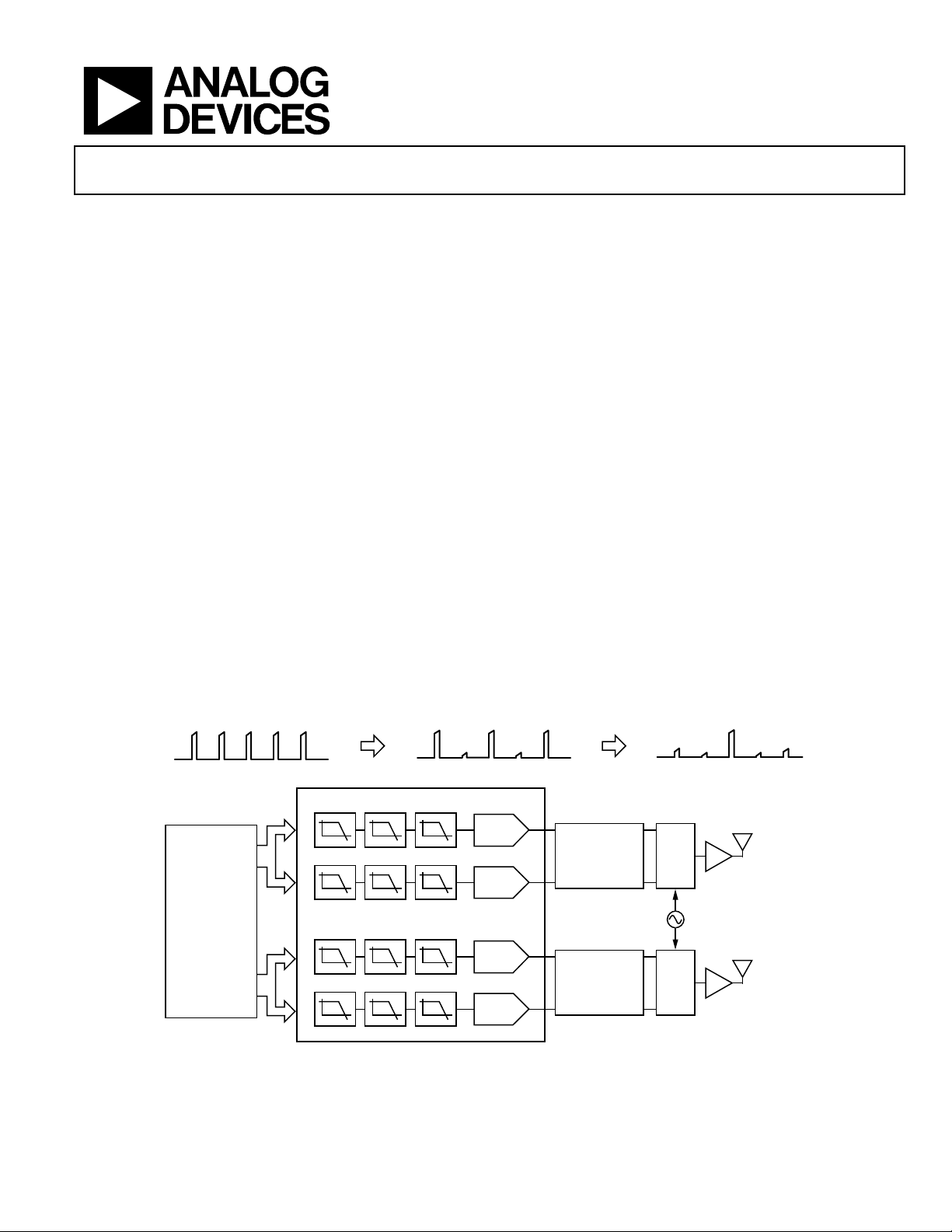
TYPICAL SIGNAL CHAIN
COMPLEX BASEBAND COMPLEX IF RF
TxDAC+ Digital-to-Analog Converter
AD9148
GENERAL DESCRIPTION
The AD9148 is a quad, 16-bit, high dynamic range, digital-toanalog converter (DAC) that provides a sample rate of 1000 MSPS.
This device includes features optimized for direct conversion
transmit applications, including gain, phase, and offset compensation. The DAC outputs are optimized to interface seamlessly with
analog quadrature modulators such as the ADL5371/ADL5372/
ADL5373/ADL5374/ADL5375. A serial peripheral interface (SPI)
is provided for programming of the internal device parameters.
Full-scale output current can be programmed over a range of 8.7 mA
to 31.7 mA. The device operates from 1.8 V and 3.3 V supplies
for a total power consumption of 3 W at the maximum sample
rate. The AD9148 is enclosed in a 196-ball chip scale package ball
grid array with the option of an attached heat spreader.
PRODUCT HIGHLIGHTS
1. Low noise and intermodulation distortion (IMD) enable
high quality synthesis of wideband signals from baseband
to high intermediate frequencies.
2. A proprietary DAC output switching technique enhances
dynamic performance.
3. The current outputs are easily configured for various
single-ended or differential circuit topologies.
4. The LVDS data input interface includes FIFO to ease input
timing.
DC
DIGITAL INTERPOL ATION F ILTERS
↑2 ↑2 ↑2
↑2 ↑2 ↑2
FPGA/ASI C/DSP
↑2 ↑2 ↑2
↑2 ↑2 ↑2
NOTES
1. AQM = ANALO G QUADRATURE MO DULATOR.
Rev. A
Information furnished by Analog Devices is believed to be accurate and reliable. However, no
responsibility is assumed by Analog Devices for its use, nor for any infringements of patents or other
rights of third parties that may result from its use. Specifications subject to change without notice. No
license is granted by implication or otherwise under any patent or patent rights of Analog Devices.
Trademarks and registered trademarks are the property of their respective owners.
LO ±
PA
PA
f
IF
f
IF
DAC1
POST DAC
ANALOG FI LTER
DAC2
DAC3
POST DAC
DAC4
Figure 1.
One Technology Way, P.O. Box 9106, Norwood, MA 02062-9106, U.S.A.
Tel: 781.329.4700 www.analog.com
Fax: 781.461.3113 ©2010–2011 Analog Devices, Inc. All rights reserved.
AQM
LO
LO
AQM
08910-001

AD9148 Data Sheet
TABLE OF CONTENTS
Features.............................................................................................. 1
Applications....................................................................................... 1
General Description ......................................................................... 1
Product Highlights ........................................................................... 1
Typical Signal Chain......................................................................... 1
Revision History ............................................................................... 3
Functional Block Diagram .............................................................. 4
Specifications..................................................................................... 5
DC Specifications ......................................................................... 5
Input/Output Signal Specifications............................................ 6
Digital Input Data Timing Specifications ................................. 7
AC Specifications.......................................................................... 8
Absolute Maximum Ratings............................................................ 9
Thermal Resistance ...................................................................... 9
Maximum Safe Power Dissipation............................................. 9
ESD Caution.................................................................................. 9
Pin Configurations and Function Descriptions ......................... 11
Typical Performance Characteristics ........................................... 15
Terminology .................................................................................... 21
Serial Peripheral Interface ............................................................. 22
General Operation of the Serial Interface............................... 22
Data Format ................................................................................22
SPI Pin Descriptions ..................................................................22
SPI Options .................................................................................23
SPI Register Map............................................................................. 24
SPI Register Descriptions.......................................................... 26
Input Data Ports.............................................................................. 40
Dual-Port Mode.......................................................................... 40
Single-Port Mode........................................................................ 40
Byte Mode.................................................................................... 41
Data Interface Options ..............................................................41
Recommended Frame Input Bias Circuitry............................ 41
FIFO Operation ..............................................................................42
Synchronizing and Resetting the FIFO ................................... 43
Monitoring the FIFO Status...................................................... 44
Device Synchronization................................................................. 45
Synchronizing Multiple Devices .............................................. 45
Synchronization with Clock Multiplication............................... 45
Synchronization with Direct Clocking.................................... 47
Additional Synchronization Features ...................................... 48
Interface Timing............................................................................. 49
Digital Data Path ............................................................................ 50
Premodulation............................................................................ 50
Programmable Inverse Sinc Filter............................................ 50
Interpolation Filters ................................................................... 51
Fine Modulation......................................................................... 54
Quadrature Phase Correction................................................... 55
DC Offset Correction ................................................................ 55
Digital Gain Control.................................................................. 55
Clock Generation ........................................................................... 56
DAC Input Clock Configurations............................................ 56
Driving the CLK_x and REFCLK_x Inputs............................ 56
Direct Clocking .......................................................................... 56
Clock Multiplication.................................................................. 57
Analog Outputs............................................................................... 59
Transmit DAC Operation.......................................................... 59
Auxiliary DAC Operation......................................................... 60
Interfacing to Modulators ......................................................... 61
Device Power Dissipation.............................................................. 63
Temperature Sensor ....................................................................... 65
Interrupt Request Operation ........................................................ 66
Interrupt Service Routine.......................................................... 66
Interface Timing Validation.......................................................... 67
SED Operation............................................................................ 67
SED Example .............................................................................. 67
Example Start-Up Routine ............................................................ 68
Derived PLL Settings ................................................................. 68
Derived NCO Settings ............................................................... 68
Start-Up Sequence...................................................................... 68
Device Verification Sequence ................................................... 68
Outline Dimensions....................................................................... 69
Ordering Guide .......................................................................... 70
Rev. A | Page 2 of 72

Data Sheet AD9148
REVISION HISTORY
9/11—Rev. 0 to Rev. A
Changes to General Description Section .......................................1
Deleted Input High Voltage, V
Low Voltage, V
or VIB Parameter, Table 2, and
IA
or VIB Parameter, Table 2, Input
IA
Note 2, Table 2; Renumbered Sequentially ....................................6
Added Input Voltage Range, V
or VIB Parameter, Table 2.........6
IA
Changes to Table 10 ........................................................................13
Changes to Figure 41 and Figure 42 .............................................23
Changes to 0x1E Addr, Table 12....................................................24
Deleted 0x74 Row, Table 12 ...........................................................26
Changes to PLL Control 2, Table 13 .............................................29
Changes to HB3 Control, 1E, Bit 7 Row, Table 13 ......................32
Deleted LVDS Pad Ctrl Row, Table 13..........................................38
Deleted Frame Input Levels Section and Table 15......................41
Added Recommended Frame Input Bias Circuitry Section and
Figure 45; Renumbered Sequentially............................................41
Changes to Timing Optimization Section...................................48
Added Table 15 ................................................................................ 48
Changes to Filter Implementation Section ..................................50
Changes to Figure 74 ......................................................................57
Deleted Test Access Port Section, Table 27, Figure 92, and
Table 28.............................................................................................68
Changes to Start-Up Sequence Section........................................ 68
Deleted Figure 93 ............................................................................69
Deleted Table 29 ..............................................................................70
6/10—Revision 0: Initial Version
Rev. A | Page 3 of 72
AD9148 Data Sheet
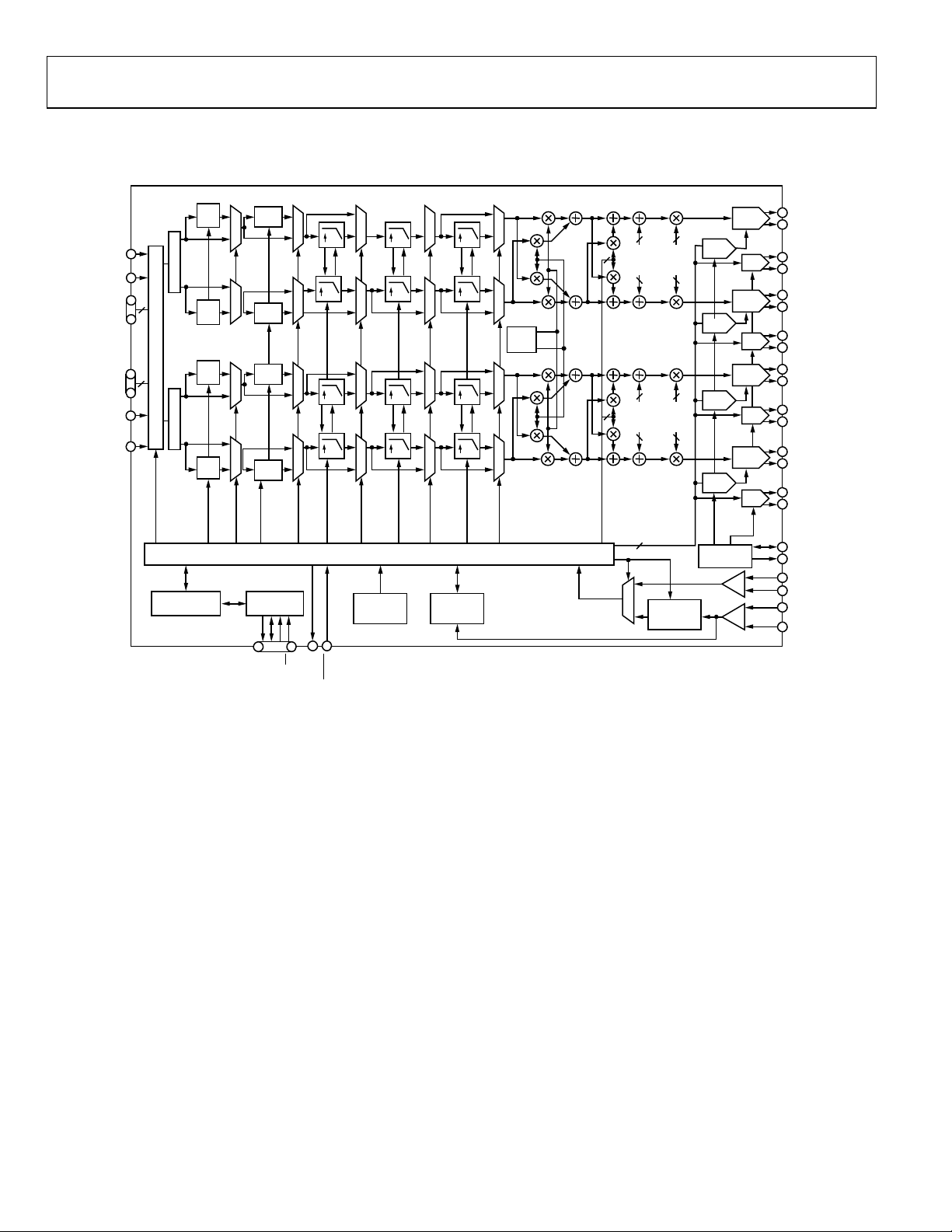
FUNCTIONAL BLOCK DIAGRAM
310MHz/620MHz 500MHz/1GHz 500MHz/1GHz
310MHz
–1
SINC
2× 2×
2× 2× 2×
–1
SINC
–1
SINC
2× 2×
2× 2×
–1
SINC
HB1_EN
HB1_CLK
INVSINE_EN
FILTER
COEFFI CIENT
INTERNA L CLOCK TIMING AND CON TRO L LOGI C
SERIAL
IN/OUT PORT
POWER-O N
RESET
1GHz
16-BIT
2×
COS
32-BIT
SIN
NCO
2×
2×
HB3_EN
HB3_CLK
HB2_EN
HB2_CLK
MULTI-CHIP
SYNC
SYNC
PHASE
CORRECTION
DAC_CLK
GAIN/
OFFSET_CTRL
PLL_CTRL
I OFFSET
Q OFFSET
I OFFSET
Q OFFSET
I GAIN
Q GAIN
I GAIN
Q GAIN
CLOCK
MULTIPLIER
(2× – 16×)
GAIN
16-BIT
GAIN
16-BIT
GAIN
16-BIT
GAIN
REFERENCE
BIAS
DAC1
DAC2
DAC3
DAC4
AUX1
AUX2
AUX3
AUX4
IOUT1_P
IOUT1_N
AUX1_P
AUX1_N
IOUT2_P
IOUT2_N
AUX2_P
AUX2_N
IOUT3_P
IOUT3_N
AUX3_P
AUX3_N
IOUT4_P
IOUT4_N
AUX4_P
AUX4_N
VREF
I120
CLK_P
CLK_N
REFCLK_P/
SYNC_P
REFCLK_N/
SYNC_N
DCIA_P/
DCIA_N
FRAMEA_P/
FRAMEA_N
A[15:0]_P/
A[15:0]_N
B[15:0]_P/
B[15:0]_N
FRAMEB_P/
FRAMEB_N
DCIB_P/
DCIB_N
1.2GHz
16
DATA RECEIVER
16
MODE
PROGRAMMING
REGISTERS
310MHz
f
/2
S
MOD
FIFO
f
/2
S
MOD
f
/2
S
MOD
FIFO
f
/2
S
MOD
PREMOD_EN
PREMOD_CLK
CS
SDO
IRQ
SDIO
SCLK
RESET
08910-002
Figure 2.
Rev. A | Page 4 of 72
Data Sheet AD9148
SPECIFICATIONS
DC SPECIFICATIONS
T
to T
MIN
otherwise noted.
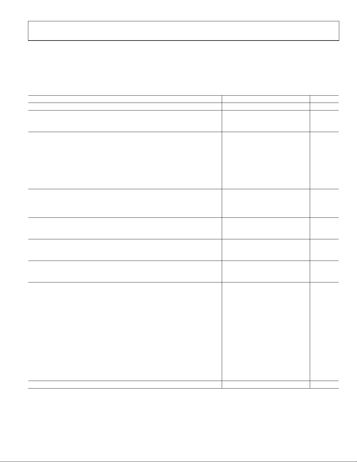
Table 1.
Parameter Min Typ Max Unit
RESOLUTION 16 Bits
ACCURACY
Differential Nonlinearity (DNL) ±2.1 LSB
Integral Nonlinearity (INL) ±3.7 LSB
MAIN DAC OUTPUTS
Offset Error ±0.001 % FSR
Gain Error (with Internal Reference) ±2 % FSR
Full-Scale Output Current1 8.66 20.2 31.66 mA
Output Compliance Range −1.0 +1.0 V
Output Resistance 10 MΩ
Gain DAC Monotonicity Guaranteed
Settling Time to Within ±0.5 LSB 20 ns
TEMPERATURE DRIFT
Main DAC Offset 0.04 ppm/°C
Main DAC Gain 100 ppm/°C
Reference Voltage 30 ppm/°C
REFERENCE
Internal Reference Voltage 1.2 V
Output Resistance 5 kΩ
ANALOG SUPPLY VOLTAGES
AVDD33 3.13 3.3 3.47 V
CVDD18 1.71 1.8 1.89 V
DIGITAL SUPPLY VOLTAGES
IOVDD 1.71 1.8/3.3 3.47 V
DVDD18 1.71 1.8 1.89 V
POWER CONSUMPTION (NCO OFF, PLL DISABLED, AND SINC−1 FILTER BYPASSED,
UNLESS OTHERWISE NOTED)
1 × Mode, f
2 × Mode, f
4 × Mode, f
4 × Mode, f
4 × Mode, f
4 × Mode, f
8 × Mode, f
Power-Down Mode 1 12 mW
OPERATING RANGE −40 +25 +85 °C
1
Based on a 10 k external resistor.
, AVDD33 = 3.3 V, IOVDD = 3.3 V, DVDD18 = 1.8 V, CVDD18 = 1.8 V, I
MAX
= 20 mA, maximum sample rate, unless
OUTFS
= 300 MSPS, f
DAC
= 500 MSPS, f
DAC
= 800 MSPS, f
DAC
= 800 MSPS, f
DAC
= 800 MSPS, f
DAC
= 800 MSPS, f
DAC
= 800 MSPS, f
DAC
= 600 MSPS 0.79 W
INTERFACE
= 500 MSPS 1.49 W
INTERFACE
= 400 MSPS 2.18 W
INTERFACE
= 400 MSPS, NCO On 2.47 W
INTERFACE
= 400 MSPS, PLL Enabled 2.26 W
INTERFACE
= 400 MSPS, Sinc−1 Filter Enabled 2.44 W
INTERFACE
= 200 MSPS 2.01 2.16 W
INTERFACE
AVDD33 368 373 mW
CVDD18 261 280 mW
IOVDD 0.8 1.6 mW
DVDD18 1377 1504 mW
Rev. A | Page 5 of 72

AD9148 Data Sheet
INPUT/OUTPUT SIGNAL SPECIFICATIONS
T
to T
MIN
otherwise noted. LVDS driver and receiver are compliant to the IEEE-1596 reduced range link, unless otherwise noted.
Table 2.
Parameter Min Typ Max Unit
CMOS INPUT LOGIC LEVEL (SCLK, SDIO, CS, RESET, TMS, TDI, TCK)
Input VIN Logic High (IOVDD = 1.8 V) 1.2 V
Input VIN Logic High (IOVDD = 3.3 V) 2.0 V
Input VIN Logic Low (IOVDD = 1.8 V) 0.6 V
Input VIN Logic Low (IOVDD = 3.3 V) 0.8 V
CMOS OUTPUT LOGIC LEVEL (SDIO, SDO, IRQ, PLL_LOCK, TDO)
Output V
Output V
Output V
Output V
LVDS RECEIVER INPUTS (A[15:0]_x, B[15:0]_x, DCIA_x, DCIB_x)
Input Voltage Range, VIA or VIB 825 1575 mV
Input Differential Threshold, V
Input Differential Hysteresis, V
Receiver Differential Input Impedance, RIN 80 120 Ω
LVDS Input Rate, f
LVDS RECEIVER INPUTS (FRAMEA_x, FRAMEB_x)
Input Voltage Range, VIA or VIB 825 1575 mV
DAC CLOCK INPUT (CLK_P, CLK_N)
Differential Peak-to-Peak Voltage 100 500 2000 mV
Common-Mode Voltage (Self-Biasing, AC-Coupled) 1.25 V
Maximum Clock Rate 1000 MSPS
REFERENCE CLOCK INPUT (REFCLK_x/SYNC_x)
Differential Peak-to-Peak Voltage 100 500 2000 mV
Common-Mode Voltage (Self-Biasing, AC-Coupled) 1.25 V
Maximum Clock Rate 500 MSPS
Minimum Clock Rate (PLL Enabled)
SERIAL PERIPHERAL INTERFACE
Maximum Clock Rate (SCLK) 40 MHz
Minimum Pulse Width High (t
Minimum Pulse Width Low (t
Set-Up Time, SDI to SCLK (tDS) 1.9 ns
Hold Time, SDI to SCLK (tDH) 0.2 ns
Data Valid, SDO to SCLK (tDV) 23 ns
Setup time, CS to SCLK (t
, AVDD33 = 3.3 V, IOVDD = 3.3 V, DVDD18 = 1.8 V, CVDD18 = 1.8 V, I
MAX
= 20 mA, maximum sample rate, unless
OUTFS
Logic High (IOVDD = 1.8 V) 1.4 V
OUT
Logic High (IOVDD = 3.3 V) 2.4 V
OUT
Logic Low (IOVDD = 1.8 V) 0.4 V
OUT
Logic Low (IOVDD = 3.3 V) 0.4 V
OUT
−100 +100 mV
IDTH
to V
IDTHH
(See Table 4) 1200 MSPS
INTERFACE
20 mV
IDTHL
Loop Divider = /2 125 MSPS
Loop Divider = /4 62.5 MSPS
Loop Divider = /8 31.25 MSPS
Loop Divider = /16 15.625 MSPS
) 12.5 ns
PWH
) 12.5 ns
PWL
DCSB
)
1.4 ns
Rev. A | Page 6 of 72
Data Sheet AD9148
DIGITAL INPUT DATA TIMING SPECIFICATIONS
Table 3.
Parameter Min Typ Max Unit
LATENCY (DACCLK CYCLES)
1× Interpolation (with or Without Coarse Modulation) 64 Cycles
2× Interpolation (with or Without Coarse Modulation) 125 Cycles
4× Interpolation (with or Without Coarse Modulation) 254 Cycles
8× Interpolation (with or Without Coarse Modulation) 508 Cycles
Inverse Sinc (1× Interpolation) 10 Cycles
Inverse Sinc (2× Interpolation) 20 Cycles
Inverse Sinc (4× Interpolation) 40 Cycles
Inverse Sinc (8× Interpolation) 80 Cycles
Fine Modulation 12 Cycles
Power–Up Time 100 ms
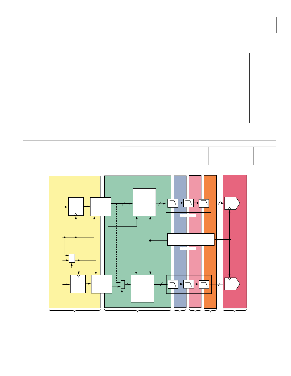
Table 4. Maximum Rate
Interface Mode f
f
INTERFACE
Dual Port Mode 620 310 620 1000 1000 1000
Single Port Mode or Byte Mode 1200 300 600 1000 1000 1000
Maximum Rate (MSPS)
f
DATA
HB1
f
f
HB2
f
HB3
DAC
DAC1
DATA
PORT A
DCIA
DCIB
DATA
PORT B
INPUT
LATCH
ONE DCI
INPUT
LATCH
f
INTERFACE
DATA
ASSEMBLER
DATA
ASSEMBLER
32
WRITE PTR A
WRITE PTR B
32 32
INTERFACE
MODE
f
DATA
FIFO A
FIFO B
32
2×
A
R
T
P
D
A
E
R
B
R
T
P
D
A
E
R
2×
2×
DATAPATH
CLK GENERATOR
AND DISTRIBUTO R
DATAPATH
2×
f
HB1
f
HB2
2×
2×
32
AND
DAC2
DACCLK
32
DAC3
AND
DAC4
f
HB3
f
DAC
08910-003
Figure 3. Defining Maximum Rates
Rev. A | Page 7 of 72

AD9148 Data Sheet
AC SPECIFICATIONS
T
to T
MIN
otherwise noted.
Table 5.
Parameter Min Typ Max Unit
SPURIOUS-FREE DYNAMIC RANGE (SFDR)
f
DAC
f
DAC
f
DAC
TWO-TONE INTERMODULATION DISTORTION (IMD)
f
DAC
f
DAC
f
DAC
NOISE SPECTRAL DENSITY (NSD) EIGHT-TONE, 500 kHz TONE SPACING
f
DAC
f
DAC
f
DAC
W-CDMA ADJACENT CHANNEL LEAKAGE RATIO (ACLR), SINGLE CARRIER
f
DAC
f
DAC
f
DAC
f
DAC
W-CDMA ALTERNATE CHANNEL LEAKAGE RATIO, SINGLE CARRIER
f
DAC
f
DAC
f
DAC
f
DAC
, AVDD33 = 3.3 V, IOVDD = 3.3 V, DVDD18 = 1.8 V, CVDD18 = 1.8 V, I
MAX
= 400 MSPS, f
= 600 MSPS, f
= 1000 MSPS, f
= 400 MSPS, f
= 600 MSPS, f
= 1000 MSPS, f
= 200 MSPS, f
= 400 MSPS, f
= 800 MSPS, f
= 737.28 MSPS, f
= 737.28 MSPS, f
= 737.28 MSPS, f
= 737.28 MSPS, f
= 737.28 MSPS, f
= 737.28 MSPS, f
= 737.28 MSPS, f
= 737.28 MSPS, f
= 80 MHz 72 dBc
OUT
= 100 MHz 67 dBc
OUT
= 100 MHz 65 dBc
OUT
= 100 MHz 85 dBc
OUT
= 120 MHz 82 dBc
OUT
= 150 MHz 76 dBc
OUT
= 80 MHz −160 dBm/Hz
OUT
= 100 MHz −161 dBm/Hz
OUT
= 100 MHz −162.5 dBm/Hz
OUT
= 100 MHz, PLL Off −81 dBc
OUT
= 100 MHz, PLL On −78 dBc
OUT
= 200 MHz, PLL Off −79 dBc
OUT
= 200 MHz, PLL On −72.5 dBc
OUT
= 100 MHz, PLL Off −87 dBc
OUT
= 100 MHz, PLL On −83 dBc
OUT
= 200 MHz, PLL Off −84 dBc
OUT
= 200 MHz, PLL On −80.5 dBc
OUT
= 20 mA, maximum sample rate, unless
OUTFS
Rev. A | Page 8 of 72
Data Sheet AD9148
(
)
(
)
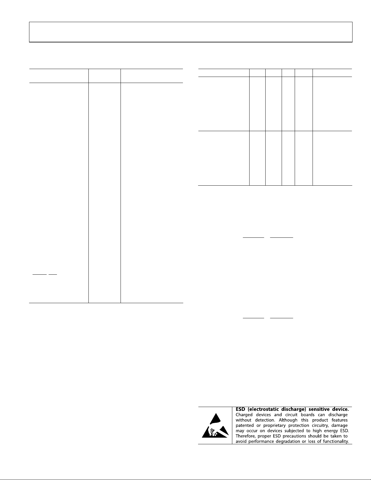
ABSOLUTE MAXIMUM RATINGS
Table 7. Thermal Resistance Table 6.
With
Parameter
AVDD33, IOVDD
DVDD18, CVDD18
AGND
DGND
CGND
I120, VREF AGND −0.3 V to AVDD33 + 0.3 V
IOUT1_P, IOUT1_N,
IOUT2_P, IOUT2_N,
IOUT3_P, IOUT3_N,
IOUT4_P, IOUT4_N
A15_P to A0_P,
A15_N to A0_N,
B15_P to B0_P,
B15_N, B0_N
DCIA_P, DCIA_N,
FRAMEA_P, FRAMEA_N,
DCIB_P, DCIB_N,
FRAMEB_P, FRAMEB_N
CLK_P, CLK_N,
REFCLK_P, REFCLK_N
CSB, SCLK, SDIO, SDO,
TDO, TDI, TCK, TMS,
RESET, IRQ, PLL_LOCK
Junction Temperature 125°C
Storage Temperature
Range
Respect To Ratin g
AGND,
DGND,
CGND
AGND,
DGND,
CGND
DGND,
CGND
AGND,
CGND
AGND,
DGND
AGND −1.0 V to AVDD33 + 0.3 V
DGND −0.3 V to DVDD18 + 0.3 V
DGND −0.3 V to DVDD18+ 0.3 V
CGND −0.3 V to CVDD18 + 0.3 V
DGND −0.3 V to IOVDD + 0.3 V
−65°C to +150°C
−0.3 V to +3.6 V
−0.3 V to +2.10 V
−0.3 V to +0.3 V
−0.3 V to +0.3 V
−0.3 V to +0.3 V
Stresses above those listed under Absolute Maximum Ratings
may cause permanent damage to the device. This is a stress
rating only; functional operation of the device at these or any
other conditions above those indicated in the operational
section of this specification is not implied. Exposure to absolute
maximum rating conditions for extended periods may affect
device reliability.
THERMAL RESISTANCE
Typical θJA, θJB, and θJC are specified vs. the number of PCB layers in
still air for each package offering. Airflow increases heat dissipation
effectively reducing θ
and θJB.
JA
Rev. A | Page 9 of 72
Package Type θ
196-Ball CSP_BGA 24.7 12.6 5.7 °C/W
19.2 10.9 5.3 °C/W
18.1 10.5 5.3 °C/W
18.0 10.5 5.3 °C/W
196-Ball BGA_ED 20.9 8.6 3.1 °C/W
16.2 7.7 3.1 °C/W
15.2 7.4 3.1 °C/W
15.0 7.4 3.1 °C/W
MAXIMUM SAFE POWER DISSIPATION
The maximum junction temperature for the AD9148 is 125°C.
With the thermal resistance of the molded package (CSP_BGA)
given for a 12 layer board, the maximum power that can be
dissipated in this package can be calculated as
Power
=
MAX
To increase the maximum power, the AD9148 is available in a
second package option (BGA_ED), which includes a heat spreader
on top of the package. Also, an external heat sink can be attached to
the top of the AD9148 CSP_BGA package. The adjusted maximum
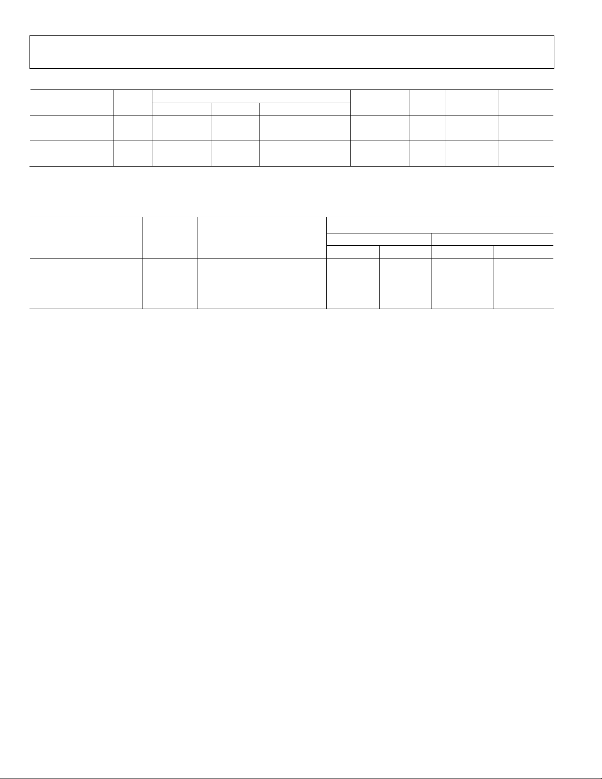
power for each of these conditions is shown in Tab le 8.
With the thermal resistance of the heat spreader package (BGA_ED)
given for a 12-layer board, the maximum power that can be
dissipated in this package can be calculated as
Power
=
MAX
To increase the maximum power, an external heat sink can be
attached to the top of the AD9148 BGA_ED package. The adjusted
maximum power for an external heat sink is shown in Tabl e 8.
To aid in the selection of package, the maximum f
power dissipation over several operating conditions is shown in
Tabl e 9. The maximum f
Note that, if the programmable inverse sinc filter is enabled, the
maximum f
rate specified in Ta b le 9 decreases.
DAC
ESD CAUTION
θ
JA
JB θJC
−
TT
J
θ
−
J
θ
()
A
=
JA
TT
()
A
=
JA
rate applies to all interpolation rates.
DAC
Unit Notes
85125=−
0.18
85125=−
0.15
W
22.2
W
67.2
DAC
4-layer board,
25 PCB vias
8-layer board,
25 PCB vias
10-layer board,
25 PCB vias
12-layer board,
25 PCB vias
4-layer board,
25 PCB vias
8-layer board,
25 PCB vias
10-layer board,
25 PCB vias
12-layer board,
25 PCB vias
rate for a given
AD9148 Data Sheet
Table 8. Thermal Resistance and Maximum Power
PCB
Package Type TA (°C) PCB Layers PCB Vias External Heat Sink1 Case TJ (°C) θJA (°C/W)
196-ball CSP_BGA 85 12 25 No CSP_BGA 125 18.0 2.22
196-ball CSP_BGA 85 12 25 Yes CSP_BGA 125 16.0 2.50
196-ball BGA_ED 85 12 25 No BGA_ED 125 15.0 2.67
196-ball BGA_ED 85 12 25 Yes BGA_ED 125 14.0 2.86
1
Heat sink is used in the thermal model: 13 mm × 13 mm, 15 mm tall.
Maximum
Power (W)
Table 9. Power vs. f
Rate and Functionality
DAC
Maximum f
(MSPS)1
DAC
Coarse Modulation Fine Modulation (NCO)
Maximum Power (W) Package Heat-Sink Combination2 PLL Off PLL On PLL Off PLL On
2.22 CSP_BGA No 820 740 695 630
2.50 CSP_BGA Yes 950 875 810 740
2.67 BGA_EP No 1000 945 870 810
2.86 BGA_EP Yes 1000 1000 940 870
1
Typical maximum f
2
Heat sink is used in the thermal model: 13 mm × 13 mm, 15 mm tall.
rate with inverse sinc filter off.
DAC
Rev. A | Page 10 of 72
Data Sheet AD9148
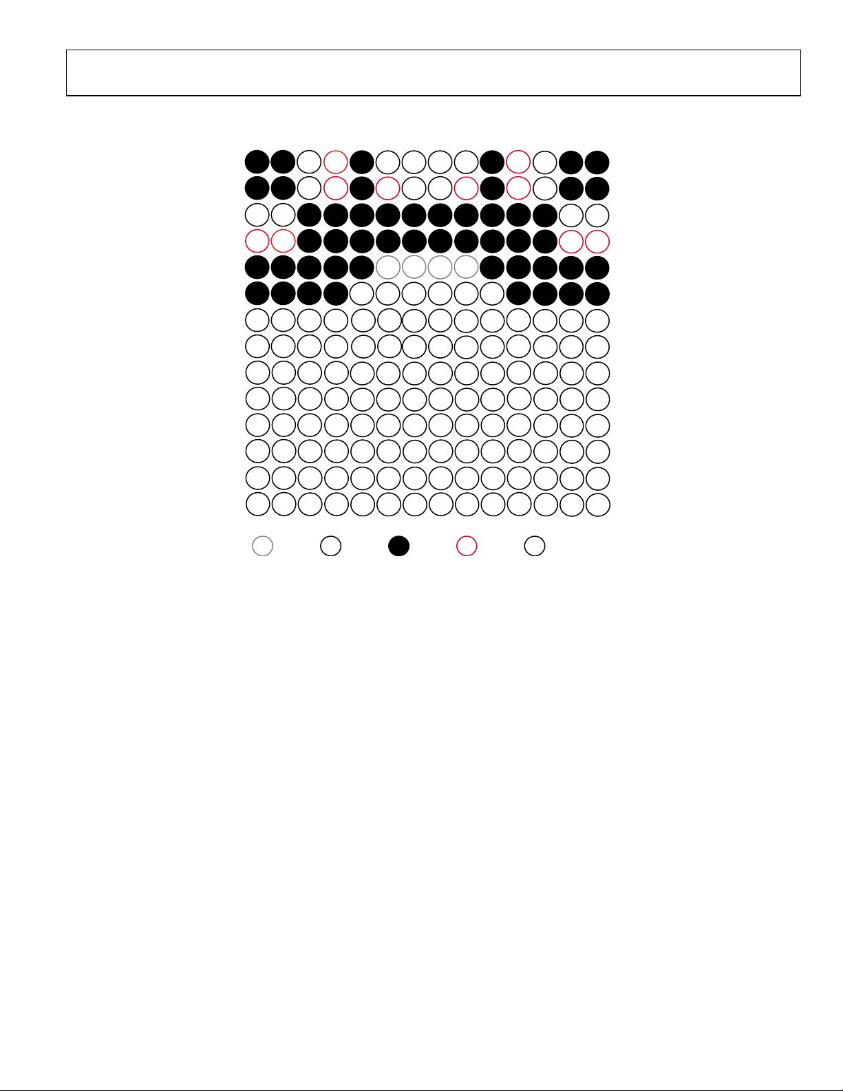
PIN CONFIGURATIONS AND FUNCTION DESCRIPTIONS
23
1
A
4
IOUT2 IOUT2
5
67
V
CLK
REF
I120
8
REF
12 13
IOUT3 IOUT3
10 11
9
14
A
NC
+
X
AVSS
NC REF
+
+
XX
9
8
AUX3 AUX3
X
10 11
POSITIVE
TERMINAL
CLKCLK
AUX4
12 13
NEGATIVE
TERMINAL
IOUT4AUX4
IOUT4
14
B
C
D
E
F
G
H
J
K
L
M
N
P
08910-004
AUX1
AUX1
23
CVDD18
+
AUX2 AUX2
4
X
B
IOUT1
C
IOUT1
D
E
F
G
H
J
K
L
M
N
P
1
XX
5
AVDD33
CLK
+
67
Figure 4. Pin Configuration (Top View), Analog and Clock Domain Pins
Rev. A | Page 11 of 72
AD9148 Data Sheet
A
B
C
D
E
F
SPI
INTERFACE
G
H
J
K
L
M
N
23
1
CSSDO
SCLK
SDIO
FrB
DCIB DCIA
DCIB
A0
A2
A0 A2
A3
RESET IRQ
B0 B2
B0 B2
B1
B1
4
++
B3
B3 B4B4B5
A5 A6A6A7
67
5
XXXXXX
XXXXXX
B5 B6B6B7
8
B7 B8 B9 B10
A8 A9 A10 A11 A12 A1 3 A1 4 A15A1
10 11
9
B8 B9 B10
Trch Trc h
B11
B11
12 13
TMS
TDONC PLL
TCK
B13
B13
B12 B14 B15
B12 B14 B15
DCIA
FrA
FrAFrB
14
A
B
C
D
E
F
TAP
INTERFACE
TDI
G
H
J
K
L
M
N
P
A1
1
+
A4A4A5
A3
23
IOVDD
X
4
5
DVDD18
A7 A8 A9 A10 A 11 A12 A13 A14 A15
67
DVSS
8
10 11
9
+LVDS –LVDS
A15A15
12 13
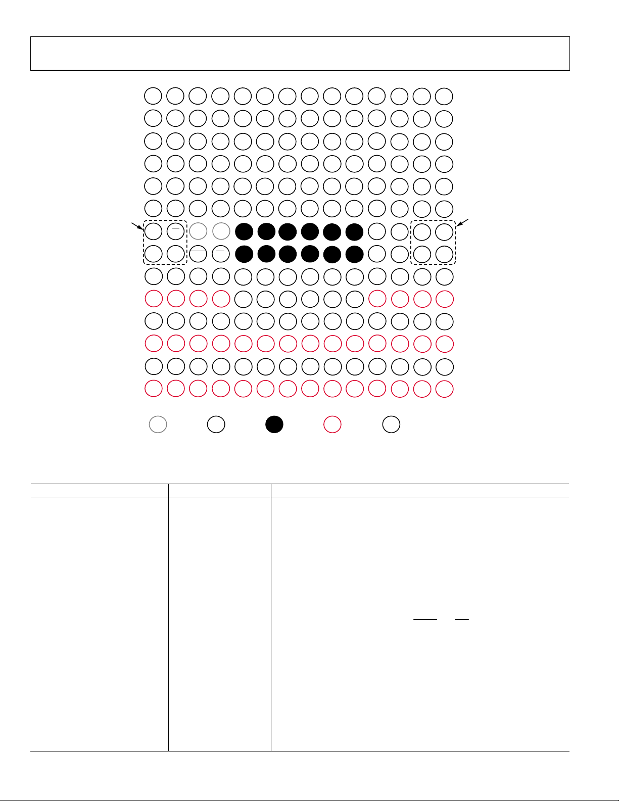
Figure 5. Pin Configuration (Top View), Digital Domain Pins
Table 10. Pin Function Description
Pin No. Mnemonic Description
E6, E7, E8, E9 CVDD18 1.8 V Clock Supply.
F5, F6, F7, F8, F9, F10 AVDD33 3.3 V Analog Supply.
A1, A2, A5, A10, A13, A14, B1,
AVSS Analog Supply Ground.
B2, B5, B10, B13, B14, C3, C4, C5,
C6, C7, C8, C9, C10, C11, C12, D3,
D4, D5, D6, D7, D8, D9, D10, D11,
D12, E1, E2, E3, E4, E5, E10, E11,
E12, E13, E14, F1, F2, F3, F4, F11,
F12, F13, F14
G5, G6, G7, G8, G9, G10, H5, H6,
DVSS Digital Supply Ground.
H7, H8, H9, H10
G3, G4 IOVDD
Supply for Serial Ports (SPI and TAP), RESET
supplied to these pins.
J5, J6, J7, J8, J9, J10, K5, K6, K7,
DVDD18 1.8 V Digital Supply.
K8, K9, K10
B7, B8, H11 NC No Connect. Do not connect to this pin.
C1 IOUT1_N DAC 1 Complementary Output Current.
D1 IOUT1_P DAC 1 Positive Output Current.
A3 IOUT2_N DAC 2 Complementary Output Current.
A4 IOUT2_P DAC 2 Positive Output Current.
A11 IOUT3_P DAC 3 Positive Output Current.
A12 IOUT3_N DAC 3 Complementary Output Current.
Rev. A | Page 12 of 72
P
14
08910-005
and IRQ. 1.8 V to 3.3 V can be

Data Sheet AD9148
Pin No. Mnemonic Description
C14 IOUT4_N DAC 4 Complementary Output Current.
D14 IOUT4_P DAC 4 Positive Output Current.
C2 AUX1_N Auxiliary DAC 1 Complementary Output Current.
D2 AUX1_P Auxiliary DAC 1 Positive Output Current.
B3 AUX2_N Auxiliary DAC 2 Complementary Output Current.
B4 AUX2_P Auxiliary DAC 2 Positive Output Current.
B11 AUX3_P Auxiliary DAC 3 Positive Output Current.
B12 AUX3_N Auxiliary DAC 3 Complementary Output Current.
C13 AUX4_N Auxiliary DAC 4 Complementary Output Current.
D13 AUX4_P Auxiliary DAC 4 Positive Output Current.
A8 I120 Tie to analog ground via a 10 kΩ resistor to generate a 120 μA reference current.
A7 VREF
B6, A6 CLK_P/CLK_N Positive/Negative DAC Clock Input (CLK).
B9, A9
H4
H3
G1 SDO Serial Data Output for SPI.
G2
H1 SDIO Serial Data Input/Output for SPI.
H2 SCLK Qualifying Clock Input for SPI.
G11, G12 TRENCH Connect this pin to VSS.
H12 PLL_LOCK Active High LVCMOS Output. It indicates the lock status of the PLL circuitry.
G13 TMS Reserved for Future Use. Connect to DVSS.
G14 TDI Reserved for Future Use. Connect to DVSS.
H13 TCK Reserved for Future Use. Connect to DVSS.
H14 TDO Reserved for Future Use. Leave unconnected.
M1, L1 A0_P/A0_N LVDS Data Input Pair, Port A (LSB).
P1, N1 A1_P/A1_N LVDS Data Input Pair, Port A.
M2, L2 A2_P/A2_N LVDS Data Input Pair, Port A.
P2, N2 A3_P/A3_N LVDS Data Input Pair, Port A.
P3, N3 A4_P/A4_N LVDS Data Input Pair, Port A.
P4, N4 A5_P/A5_N LVDS Data Input Pair, Port A.
P5, N5 A6_P/A6_N LVDS Data Input Pair, Port A.
P6, N6 A7_P/A7_N LVDS Data Input Pair, Port A.
P7, N7 A8_P/A8_N LVDS Data Input Pair, Port A.
P8, N8 A9_P/A9_N LVDS Data Input Pair, Port A.
P9, N9 A10_P/A10_N LVDS Data Input Pair, Port A.
P10, N10 A11_P/A11_N LVDS Data Input Pair, Port A.
P11, N11 A12_P/A12_N LVDS Data Input Pair, Port A.
P12, N12 A13_P/A13_N LVDS Data Input Pair, Port A.
P13, N13 A14_P/A14_N LVDS Data Input Pair, Port A.
P14, N14 A15_P/A15_N LVDS Data Input Pair, Port A (MSB).
K13, J13 DCIA_P/DCIA_N LVDS Data Clock Input Pair for Port A.
K14, J14 FRAMEA_P/FRAMEA_N
K3, J3 B0_P/B0_N LVDS Data Input Pair, Port B (LSB).
M3, L3 B1_P/B1_N LVDS Data Input Pair, Port B.
K4, J4 B2_P/B2_N LVDS Data Input Pair, Port B.
M4, L4 B3_P/B3_N LVDS Data Input Pair, Port B.
M5, L5 B4_P/B4_N LVDS Data Input Pair, Port B
M6, L6 B5_P/B5_N LVDS Data Input Pair, Port B.
REFCLK_P/REFCLK_N or
SYNC_P/SYNC_N
Active Low Open-Drain Interrupt Request Output. Pull up to IOVDD with
IRQ
RESET
CS
Band Gap Voltage Reference I/O. Decouple to analog ground via a 0.1 μF
capacitor. Output impedance is approximately 5 kΩ.
PLL Reference Clock Input (REFCLK_x). This pin has a secondary function as
a synchronization input (SYNC_x).
a 10 kΩ resistor.
An active low LVCMOS input resets the device. Pull up to IOVDD.
Active Low Chip Select for SPI.
LVDS Frame Input for Port A. Tie to LVDS logic low if not used.
Recommended external bias circuit is shown in Figure 49.
Rev. A | Page 13 of 72

AD9148 Data Sheet
Pin No. Mnemonic Description
M7, L7 B6_P/B6_N LVDS Data Input Pair, Port B.
M8, L8 B7_P/B7_N LVDS Data Input Pair, Port B.
M9, L9 B8_P/B8_N LVDS Data Input Pair, Port B.
M10, L10 B9_P/B9_N LVDS Data Input Pair, Port B.
M11, L11 B10_P/B10_N LVDS Data Input Pair, Port B.
K11, J11 B11_P/B11_N LVDS Data Input Pair, Port B.
M12, L12 B12_P/B12_N LVDS Data Input Pair, Port B.
K12, J12 B13_P/B13_N LVDS Data Input Pair, Port B.
M13, L13 B14_P/B14_N LVDS Data Input Pair, Port B.
M14, L14 B15_P/B15_N LVDS Data Input Pair, Port B (MSB).
K2, J2 DCIB_P/DCIB_N LVDS Data Clock Input Pair for Port B.
K1, J1 FRAMEB_P/FRAMEB_N
LVDS Frame Input for Port B. Tie to LVDS logic low if not used.
Recommended external bias circuit is shown in Figure 49.
Rev. A | Page 14 of 72
Data Sheet AD9148
–
–
–
–
–
–
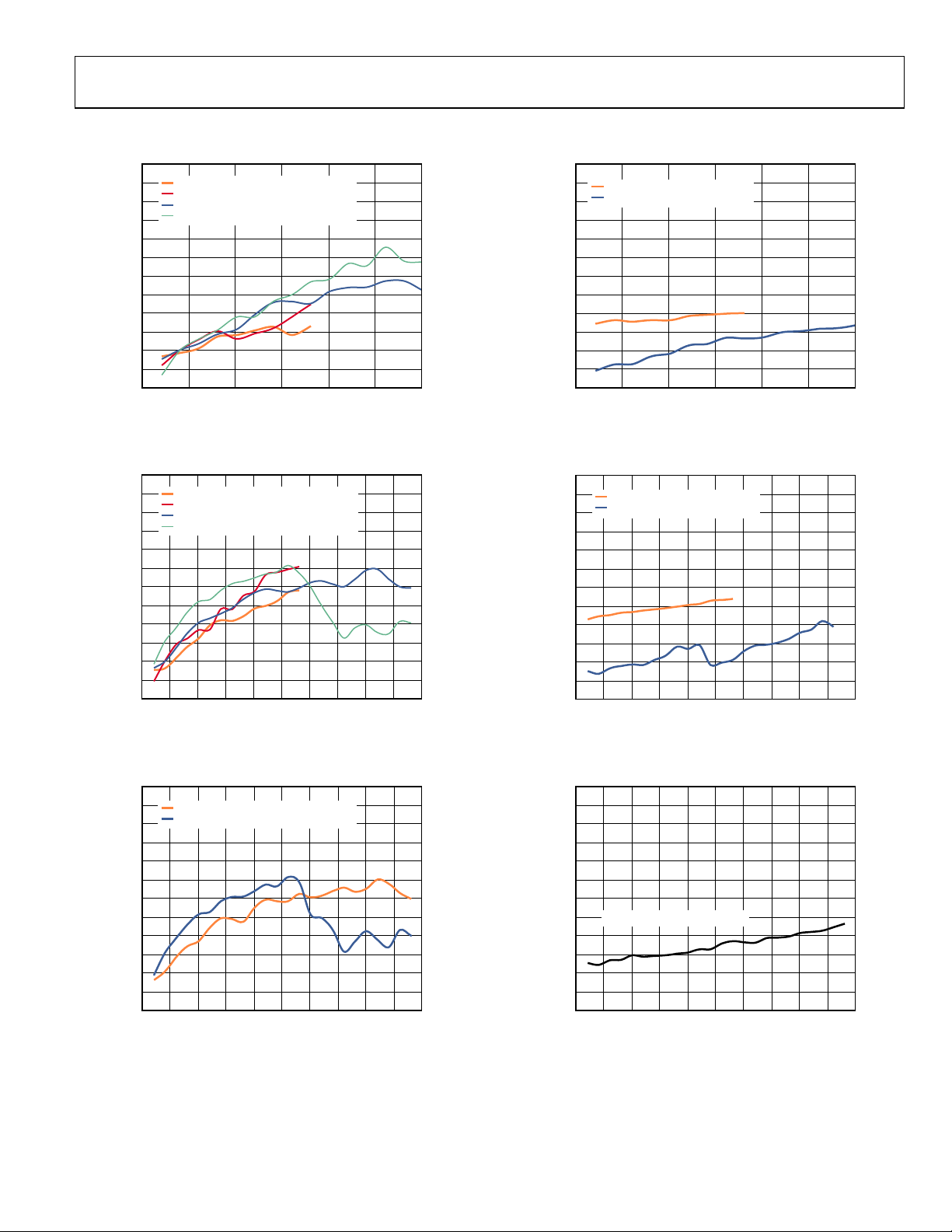
TYPICAL PERFORMANCE CHARACTERISTICS
30
–35
–40
–45
–50
–55
–60
–65
–70
HARMONIC LEVE L (dBc)
–75
–80
–85
–90
Figure 6. Harmonic Level vs. f
f
= 200MSPS, SE COND HARMONIC
DATA
f
= 200MSPS, T HIRD HARMONIC
DATA
f
= 310MSPS, SE COND HARMONIC
DATA
f
= 310MSPS, T HIRD HARMONIC
DATA
0 50 100 150 200 250 300
f
OUT
OUT
(MHz)
over f
, 2× Interpolation,
DATA
Digital Scale = 0 dBFS, Full-Scale Current = 20 mA
30
–35
–40
–45
–50
–55
–60
–65
–70
HARMONIC LEVE L (dBc)
–75
–80
–85
–90
Figure 7. Harmonic Level vs. f
f
= 150MSPS, SE COND HARMONIC
DATA
f
= 150MSPS, T HIRD HARMONIC
DATA
f
= 250MSPS, SE COND HARMONIC
DATA
f
= 250MSPS, T HIRD HARMONIC
DATA
0 50 100 150 200 250 300 350 400 450 500
f
OUT
OUT
(MHz)
over f
, 4× Interpolation,
DATA
Digital Scale = 0 dBFS, Full-Scale Current = 20 mA
30
–35
–40
–45
–50
–55
–60
–65
–70
HARMONIC LEVE L (dBc)
–75
–80
–85
–90
Figure 8. Harmonic Level vs. f
f
= 125MSPS, SE COND HARMONIC
DATA
f
= 125MSPS, T HIRD HARMONIC
DATA
0 50 100 150 200 250 300 350 400 450 500
f
(MHz)
OUT
, 8× Interpolation over f
OUT
Digital Scale = 0 dBFS, Full-Scale Current = 20 mA
= 125 MSPS,
DATA
08910-006
08910-007
08910-008
30
–35
–40
–45
–50
–55
–60
–65
–70
SPUR LEVEL (dBc)
–75
–80
–85
–90
Figure 9. Highest Digital Spur vs. f
f
= 200MSPS,
DATA
f
= 310MSPS,
DATA
0 50 100 150 200 250 300
f
DATA
f
DATA
f
OUT
+
f
OUT
+
f
OUT
(MHz)
OUT
over f
DATA
Digital Scale = 0 dBFS, Full-Scale Current = 20 mA
30
–35
–40
–45
–50
–55
–60
–65
–70
SPUR LEVEL (dBc)
–75
–80
–85
–90
Figure 10. Highest Digital Spur vs. f
f
= 150MSPS,
DATA
f
= 250MSPS, 2
DATA
0 50 100 150 200 250 300 350 400 450 500
f
DATA
f
f
OUT
DATA
+
f
–
(MHz)
OUT
OUT
f
OUT
over f
DATA
Digital Scale = 0 dBFS, Full-Scale Current = 20 mA
30
–35
–40
–45
–50
–55
–60
–65
–70
SPUR LEVEL (dBc)
–75
–80
–85
–90
Figure 11. Highest Digital Spur vs. f
f
= 125MSPS,
DATA
0 50 100 150 200 250 300 350 400 450 500
f
+
f
DATA
OUT
f
(MHz)
OUT
, 8× Interpolation, f
OUT
Digital Scale = 0 dBFS, Full-Scale Current = 20 mA
, 2× Interpolation,
, 4× Interpolation,
= 125 MSPS,
DATA
08910-009
08910-010
08910-011
Rev. A | Page 15 of 72
AD9148 Data Sheet
–
–
–
30
–35
–40
–45
–50
–55
–60
–65
–70
HARMONIC LEVE L (dBc)
–75
–80
–85
–90
Full-Scale Current = 20 mA, 4× Interpolation, f
–35
–40
–45
–50
–55
–60
–65
–70
HARMONIC LEVE L (dBc)
–75
–80
–85
–90
–10
–20
–30
–40
–50
–60
POWER LEVEL (dBm)
–70
–80
–90
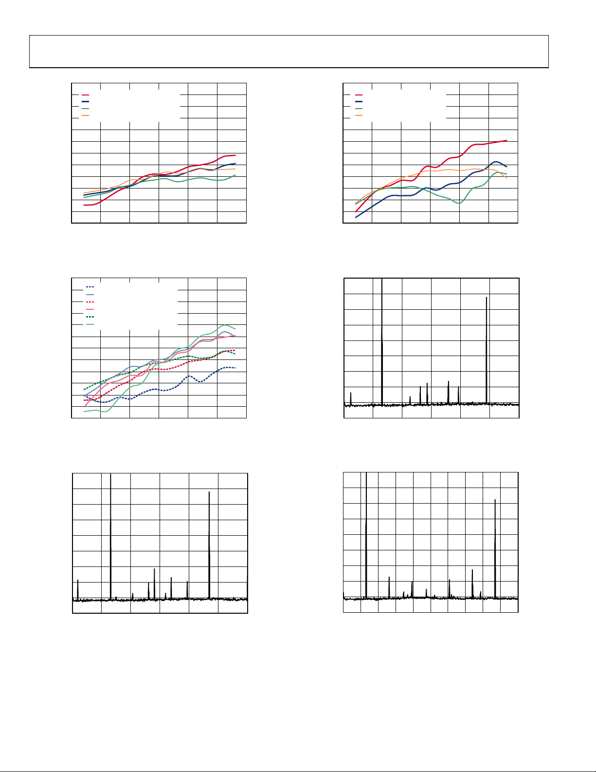
Figure 14. 4× Interpolation, f
0dBFS, SE COND HARMONIC
–6dBFS, SECOND HARMONIC
–12dBFS, SECOND HARMONIC
–18dBFS, SECOND HARMONIC
0 50 100 150 200 250 300
Figure 12. Second Harmonic vs. f
30
10mA, SECOND HARMONIC
10mA, THIRD HARMONI C
20mA, SECOND HARMONI C
20mA, THIRD HARMONI C
30mA, SECOND HARMONI C
30mA, THIRD HARMONI C
0 50 100 150 200 250 300
Figure 13. Second Harmonic vs. f
Digital Scale = 0 dBFS, 4× Interpolation, f
0
0 100 200 300 400 500 600
f
(MHz)
OUT
OUT
f
(MHz)
OUT
over Full-Scale Current,
OUT
FREQUENCY ( MHz)
= 150 MSPS, f
DATA
over Digital Scale,
DATA
= 150 MSPS
DATA
OUT
= 150 MSPS
= 131 MHz
08910-012
08910-013
08910-014
30
–35
–40
–45
–50
–55
–60
–65
–70
HARMONIC LEVE L (dBc)
–75
–80
–85
–90
Full-Scale Current = 20 mA, 4× Interpolation, f
–10
–20
–30
–40
–50
–60
POWER LEVEL (dBm)
–70
–80
–90
Figure 16. 2× Interpolation, f
0dBFS, T HIRD HARMONIC
–6dBFS, T HIRD HARMONIC
–12dBFS, T HIRD HARMONIC
–18dBFS, T HIRD HARMONIC
0 50 100 150 200 250 300
Figure 15. Third Harmonic vs. f
0
0 100 200 300 400 500 600
f
(MHz)
OUT
over Digital Scale,
OUT
FREQUENCY ( MHz)
= 310 MSPS, f
DATA
DATA
OUT
0
–10
–20
–30
–40
–50
–60
POWER LEVEL (dBm)
–70
–80
–90
0 100 200 30 0 400 500 600 700 800 900 1000
Figure 17. 8× Interpolation, f
FREQUENCY ( MHz)
= 125 MSPS, f
DATA
OUT
= 150 MSPS
= 131 MHz
= 131 MHz
08910-015
08910-016
08910-017
Rev. A | Page 16 of 72
Data Sheet AD9148
–
–
–
–
–
–
30
–35
–40
–45
IMD (dBc)
–50
–55
–60
–65
–70
–75
–80
–85
–90
–95
–100
f
= 200MSPS
DATA
f
= 310MSPS
DATA
0 50 100 150 200 250 300 350
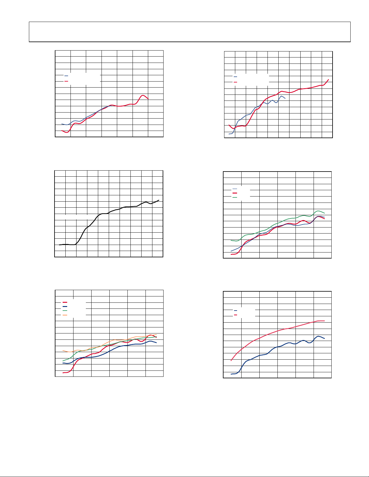
Figure 18. IMD vs. f
OUT
f
OUT
over f
(MHz)
, 2× Interpolation,
DATA
Digital Scale = 0 dBFS, Full-Scale Current = 20 mA
30
–35
–40
–45
–50
–55
–60
–65
f
= 125MSPS
DATA
–70
IMD (dBc)
–75
–80
–85
–90
–95
–100
0 50 100 150 200 250 300 350 400 450 500
Figure 19. IMD vs. f
f
(MHz)
OUT
, 8× Interpolation, f
OUT
= 125 MSPS,
DATA
Digital Scale = 0 dBFS, Full-Scale Current = 20 mA
30
–35
IMD (dBc)
–40
–45
–50
–55
–60
–65
–70
–75
–80
–85
–90
–95
–100
0dBFS
–6dBFS
–12dBFS
–18dBFS
0 50 100 150 200 250 300
Figure 20. IMD vs. f
f
= 150 MSPS, Full-Scale Current = 20 mA
DATA
f
(MHz)
OUT
over Digital Scale, 4× Interpolation,
OUT
08910-018
08910-019
08910-020
30
–35
–40
–45
IMD (dBc)
–50
–55
–60
–65
–70
–75
–80
–85
–90
–95
–100
f
= 150MSPS
DATA
f
= 250MSPS
DATA
0 50 100 150 200 250 300 350 400 450 500
Figure 21. IMD vs. f
OUT
f
OUT
over f
(MHz)
DATA
, 4× Interpolation,
Digital Scale = 0 dBFS, Full-Scale Current = 20 mA
30
–35
–40
–45
–50
–55
–60
–65
–70
IMD (dBc)
–75
–80
–85
–90
–95
–100
4× Interpolation, f
30
–35
–40
–45
–50
–55
–60
–65
–70
IMD (dBc)
–75
–80
–85
–90
–95
–100
10mA
20mA
30mA
0 50 100 150 200 250 300
Figure 22. IMD vs. f
PLL OFF
PLL ON
0 50 100 150 200 250 300
Figure 23. IMD vs. f
f
(MHz)
OUT
over Full-Scale Current,
OUT
= 150 MSPS, Digital Scale = 0 dBFS
DATA
f
(MHz)
OUT
, PLL On and Off,
OUT
Digital Scale = 0 dBFS, Full-Scale Current = 20 mA
08910-021
08910-022
08910-023
Rev. A | Page 17 of 72
AD9148 Data Sheet
–
–
–
–
–
–
144
–146
–148
–150
–152
–154
–156
NSD (dBm/Hz)
–158
–160
–162
–164
–166
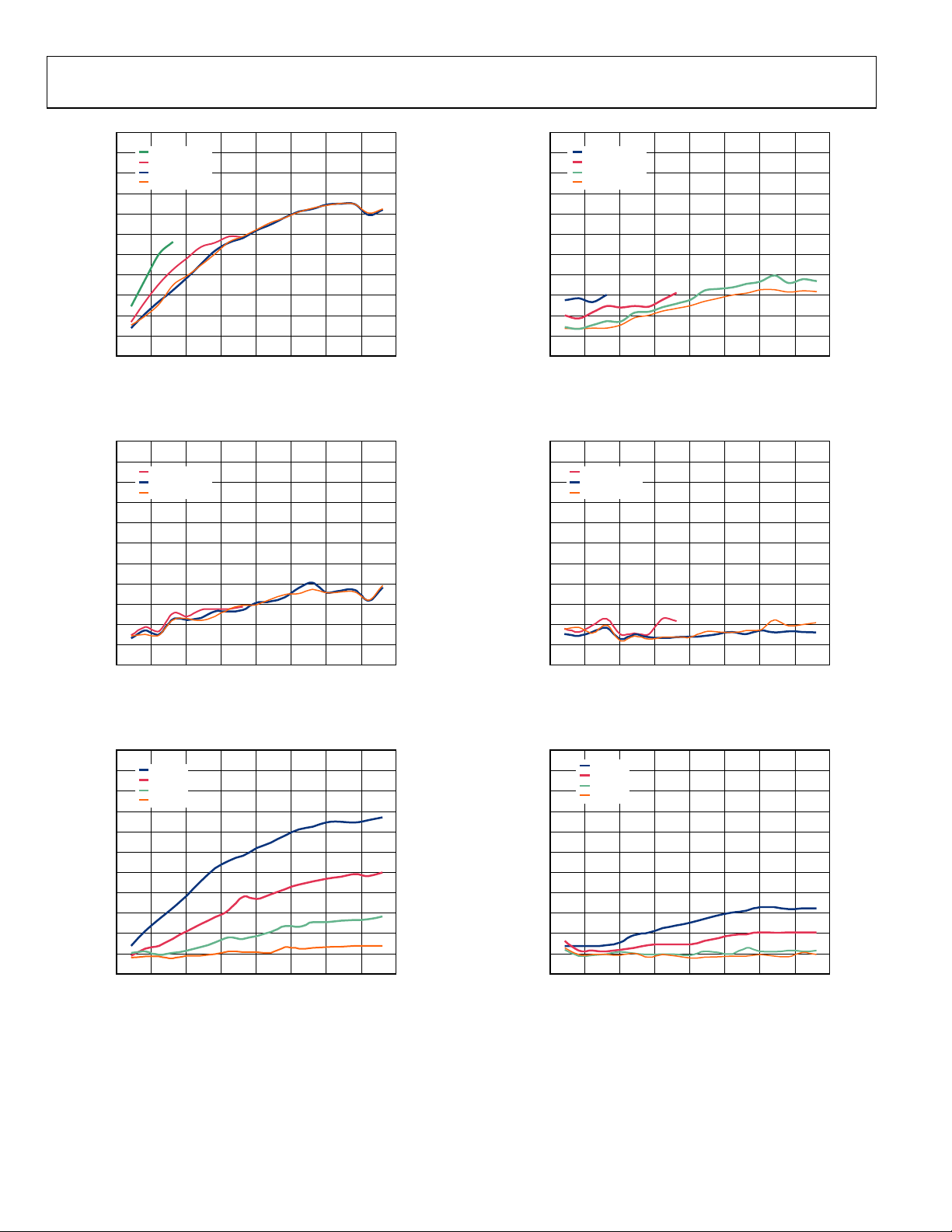
Figure 24. Single-Tone NSD Performance vs. f
144
–146
–148
–150
–152
–154
–156
NSD (dBm/Hz)
–158
–160
–162
–164
–166
Figure 25. Single-Tone NSD Performance vs. f
144
–146
–148
–150
–152
–154
–156
NSD (dBm/Hz)
–158
–160
–162
–164
–166
1×, 200MSPS
2×, 200MSPS
4×, 200MSPS
8×, 100MSPS
0 50 100 150
= 200 MSPS, Full-Scale Current = 20 mA
4× f
DATA
2×, 200MSPS
4×, 200MSPS
8×, 100MSPS
0 50 100 150
= 200 MSPS, Full-Scale Current = 20 mA, PLL On
4× f
DATA
0dB
–6dB
–12dB
–18dB
0 50 100 150 200 25 0 300 350 400
f
f
f
OUT
OUT
OUT
200
(MHz)
200
(MHz)
(MHz)
250 300
OUT
250 300
OUT
Figure 26. Single-Tone NSD Performance vs. f
= 200 MSPS, Full-Scale Current = 20 mA
4× f
DATA
350
400
, Digital Scale = 0 dBFS,
350
400
, Digital Scale = 0 dBFS,
over Digital Scale,
OUT
08910-024
08910-025
08910-026
144
–146
–148
–150
–152
–154
–156
NSD (dBm/Hz)
–158
–160
–162
–164
–166
Figure 27. Eight-Tone NSD Performance vs. f
1×, 200MSPS
2×, 200MSPS
4×, 200MSPS
8×, 100MSPS
0 50 100 150
f
OUT
200
(MHz)
250 300
, Digital Scale = 0 dBFS,
OUT
Full-Scale Current = 20 mA
144
–146
–148
–150
–152
–154
–156
NSD (dBm/Hz)
–158
–160
–162
–164
–166
Figure 28. Single-Tone NSD Performance vs. f
2×, 200MSPS
4×, 200MSPS
8×, 100MSPS
0 50 100 150
f
OUT
200
(MHz)
250 300
OUT
Full-Scale Current = 20 mA, PLL On
144
–146
–148
–150
–152
–154
–156
NSD (dBm/Hz)
–158
–160
–162
–164
–166
Figure 29. Eight-Tone NSD Performance vs. f
0dB
–6dB
–12dB
–18dB
0 50 100 150 200 25 0 300 350 400
= 200 MSPS, Full-Scale Current = 20 mA
4× f
DATA
f
OUT
(MHz)
OUT
350
400
350
400
, Digital Scale = 0 dBFS,
over Digital Scale,
08910-027
08910-028
08910-029
Rev. A | Page 18 of 72
Data Sheet AD9148
–
–
–
C
–
3
C
–
3
50
–55
–60
–65
–70
–75
ACLR (dBc)
–80
–85
–90
–95
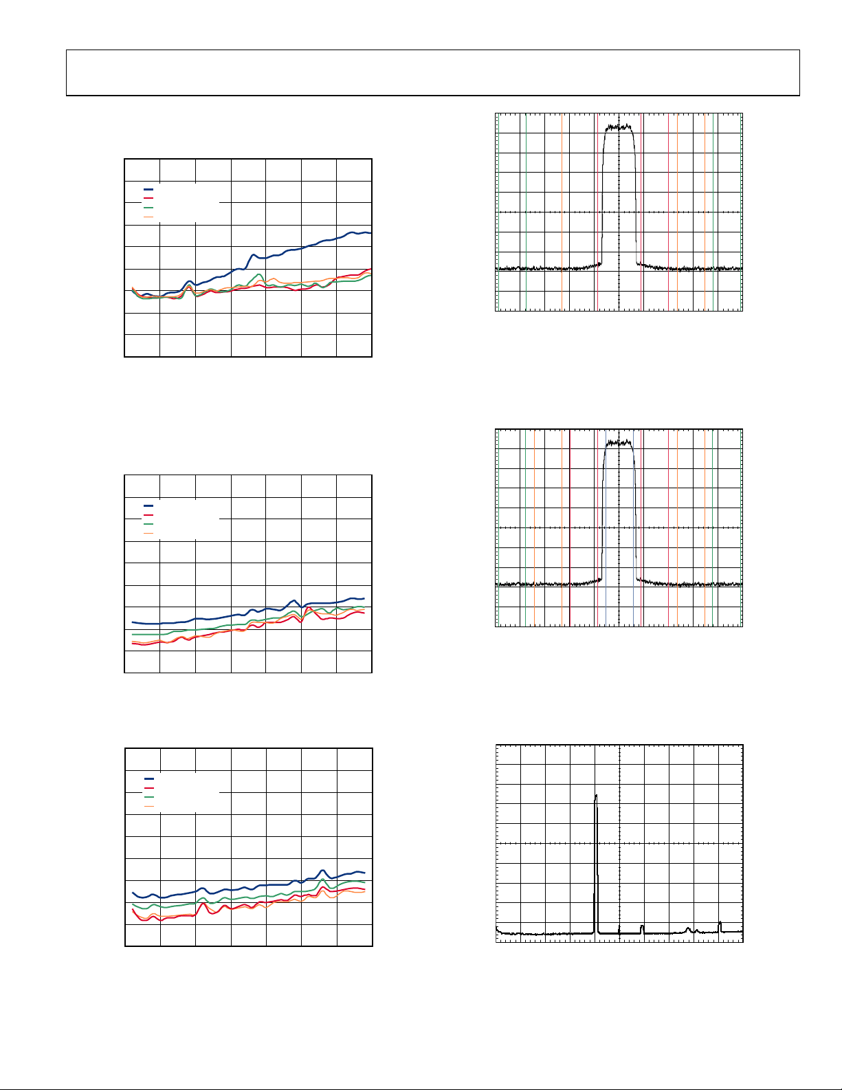
Figure 30. One-Carrier W-CDMA ACLR vs. f
50
–55
–60
–65
–70
–75
ACLR (dBc)
–80
–85
–90
–95
Figure 31. One-Carrier W-CDMA ACLR vs. f
50
–55
–60
–65
–70
–75
ACLR (dBc)
–80
–85
–90
–95
Figure 32. One-Carrier W-CDMA ACLR vs. f
0dB, PLL O N
0dB, PLL O FF
–3dB, PLL O FF
–6dB, PLL O FF
0 50 100 150 200 250 300 350
4× Interpolation, f
0dB, PLL O N
0dB, PLL O FF
–3dB, PLL O FF
–6dB, PLL O FF
0 50 100 150 200 250 300 350
4× Interpolation, f
0dB, PLL ON
0dB, PLL OF F
–3dB, PLL O FF
–6dB, PLL O FF
0 50 100 150 200 250 300 350
4× Interpolation, f
f
f
OUT
OUT
f
OUT
(MHz)
DATA
(MHz)
DATA
(MHz)
DATA
, Adjacent Channel,
OUT
= 184.32 MHz
, Alternate Channel,
OUT
= 184.32 MHz
, Second Alternate Channel,
OUT
= 184.32 MHz
CENTER 150.00MHz
#RES BW 30kHz
RMS RESULTS
ARRIER POWER 5.000MHz 3.840MHz –78.88 –92.35 –77. 98 –91.45
13.47dBm/ 10. 00MHz 3.840MHz –82.12 –95.59 –82.65 –96.12
08910-030
.84000MHz 15.00MHz 3.840MHz –82.18 –95.65 –82.28 –95.75
VBW 300kHz
FREQ
OFFSET
SWEEP 112. 5ms (601 PTS)
REF BW
Figure 33. One-Carrier W-CDMA ACLR, f
4× Interpolation, f
CENTER 150.00MHz
#RES BW 30kHz
RMS RESULTS
ARRIER POWER 5.000MHz 3.840MHz –74.50 –87.27 –73. 79 –86.56
12.77dBm/ 10. 00MHz 3.840MHz –82.72 –95.49 –82.99 –95.76
08910-031
.84000MHz 15.00MHz 3.840MHz –82.97 –95.74 –83.54 –96.31
VBW 300kHz
FREQ
OFFSET
= 184.32 MHz, PLL Off
DATA
SWEEP 112. 5ms (601 PTS)
REF BW
Figure 34. One-Carrier W-CDMA ACLR, f
4× Interpolation, f
START 1.0MHz
08910-032
#RES BW 30kHz SWEEP 1.6 85s (601 PTS)
Figure 35. One-Carrier W-CDMA, f
= 184.32 MHz, PLL On
DATA
VBW 30kHz
OUT
= 150 MHz, f
LOWER
dBc dBm
LOWER
dBc dBm
SPAN 34.68MHz
UPPER
dBc dBm
= 150 MHz,
OUT
SPAN 34.68MHz
UPPER
dBc dBm
= 150 MHz,
OUT
STOP 368. 6MHz
= 737.28 MSPS,
DAC
08910-033
08910-034
08910-035
4× Interpolation, −3 dBFS
Rev. A | Page 19 of 72
AD9148 Data Sheet
–
CENTER 150.00MHz
#RES BW 30kHz
TOTAL CARRI ER POWER –13.30 dBm/15 .3600MHz
REF CARRIER PO WER –19. 14dBm/3.84000M Hz
RCC FILTER: ON FILTER ALPHA 0.22
1 –19.14dBm
2 –19.29dBm
3 –19.24dBm
4 –19.61dBm
VBW 300kHz
FREQ
OFFSET
INTEG BW
5.000MHz 3.840MHz –72.59 –91.81 –72. 99 –92.22
10.00MHz 3.840MHz –73.58 –92.81 –74. 45 –93.67
15.00MHz 3.840MHz –75.18 –94.40 –75. 28 –94.51
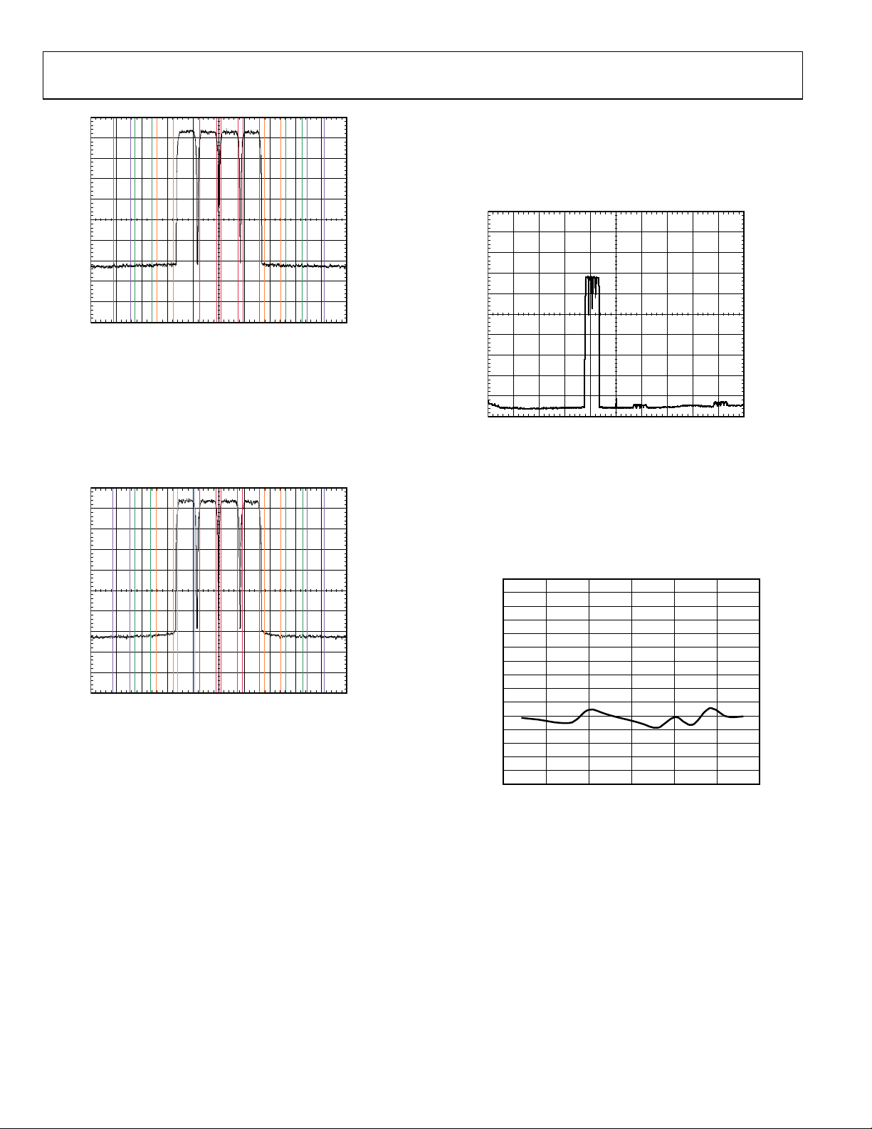
Figure 36. Four-Carrier W-CDMA, f
4× Interpolation, −3 dBFS, PLL Off
CENTER 150.00MHz
#RES BW 30kHz
TOTAL CARRI ER POWER –13.28 dBm/15 .3600MHz
REF CARRIER PO WER –19. 07dBm/3.84000M Hz
RCC FILTER: ON FILTER ALPHA 0.22
1 –19.07dBm
2 –19.42dBm
3 –19.28dBm
4 –19.45dBm
VBW 300kHz
FREQ
OFFSET
INTEG BW
5.000MHz 3.840MHz –64.50 –64.39 –83.56
10.00MHz 3.840MHz –65.12 –65.20 –84.37
15.00MHz 3.840MHz –65.40
Figure 37. Four-Carrier W-CDMA, f
4× Interpolation, −3 dBFS, PLL On
SWEEP 193. 2ms (601 PTS)
= 150 MHz, f
OUT
SWEEP 193. 2ms (601 PTS)
= 150 MHz, f
OUT
SPAN 59.58MHz
LOWER
dBc dBm
SPAN 59.58MHz
LOWER
dBc dBm
–83.67
–84.29
–84.57 –65.35 –84.52
dBc dBm
DAC
dBc dBm
DAC
UPPER
8910-036
= 737.28 MSPS,
UPPER
8910-037
= 737.28 MSPS,
START 1.0MHz
#RES BW 30kHz SWEEP 1.6 85s (601 PTS)
Figure 38. Four-Carrier W-CDMA, f
VBW 30kHz
= 150 MHz, f
OUT
STOP 368. 6MHz
= 737.28 MSPS,
DAC
4× Interpolation, −3 dBFS
80
–82
–84
–86
–88
–90
–92
–94
–96
–98
CROSSTALK (dB)
–100
–102
–104
–106
–108
–110
0 50 100 150 200 250 300
f
(MHz)
OUT
Figure 39. Crosstalk (DAC Set 1 to DAC Set 2), 4× Interpolation,
f
= 150 MSPS, Digital Scale = 0 dBFS, Full-Scale Current = 20 mA
DATA
08910-038
08910-039
Rev. A | Page 20 of 72

Data Sheet AD9148
TERMINOLOGY
Integral Nonlinearity (INL)
INL is defined as the maximum deviation of the actual analog
output from the ideal output, determined by a straight line
drawn from zero scale to full scale.
Differential Nonlinearity (DNL)
DNL is the measure of the variation in analog value, normalized
to full scale, associated with a 1 LSB change in digital input code.
Monotonicity
A DAC is monotonic if the output either increases or remains
constant as the digital input increases.
Offset Error
The deviation of the output current from the ideal of zero is called
offset error. For IOUTx_P, 0 mA output is expected when the
inputs are all 0s. For IOUTx_N, 0 mA output is expected when
all inputs are set to 1.
Gain Error
The difference between the actual and ideal output span. The
actual span is determined by the difference between the output
when all inputs are set to 1 and the output when all inputs are
set to 0.
Output Compliance Range
The range of allowable voltage at the output of a current-output
DAC. Operation beyond the maximum compliance limits can
cause either output stage saturation or breakdown, resulting in
nonlinear performance.
Temp er at u re D ri ft
Temperature drift is specified as the maximum change from the
ambient (25°C) value to the value at either T
MIN
or T
MAX
. For
offset and gain drift, the drift is reported in ppm of full-scale
range (FSR) per degrees Celsius. For reference drift, the drift is
reported in ppm per degrees Celsius.
Power Supply Rejection (PSR)
The maximum change in the full-scale output as the supplies
are varied from minimum to maximum specified voltages.
Settling Time
The time required for the output to reach and remain within a
specified error band around its final value, measured from the
start of the output transition.
In-Band Spurious Free Dynamic Range (SFDR)
The difference, in decibels, between the peak amplitude of the
output signal and the peak spurious signal between dc and the
frequency equal to half the input data rate.
Out-of-Band Spurious Free Dynamic Range (SFDR)
The difference, in decibels, between the peak amplitude of the
output signal and the peak spurious signal within the band that
starts at the frequency of the input data rate and ends at the
Nyquist frequency of the DAC output sample rate. Normally,
energy in this band is rejected by the interpolation filters. This
specification, therefore, defines how well the interpolation
filters work and the effect of other parasitic coupling paths on
the DAC output.
Total Harmonic Distortion (THD)
THD is the ratio of the rms sum of the first six harmonic components to the rms value of the measured fundamental. It is
expressed as a percentage or in decibels.
Signal-to-Noise Ratio (SNR)
SNR is the ratio of the rms value of the measured output signal
to the rms sum of all other spectral components below the
Nyquist frequency, excluding the first six harmonics and dc.
The value for SNR is expressed in decibels.
Interpolation Filter
An interpolation filter up-samples the input digital data by a
multiple of f
(interpolation rate) and then filters out the
DATA
undesired spectral images created by the up-sampling process.
Adjacent Channel Leakage Ratio (ACLR)
The ratio in dBc between the measured power within a channel
relative to its adjacent channel.
Complex Image Rejection
In a traditional two-part upconversion, two images are created
around the second IF frequency. These images have the effect of
wasting transmitter power and system bandwidth. By placing
the real part of a second complex modulator in series with the
first complex modulator, either the upper or lower frequency
image near the second IF can be rejected.
Rev. A | Page 21 of 72

AD9148 Data Sheet
S
SERIAL PERIPHERAL INTERFACE
G1
SDO
SDIO
H1
SPI
CS
PORT
G2
H2
08910-040
t
CLK
Figure 40. SPI Por
The serial port is a flexible, synchronous serial communications
port allowing easy interface to many industry-standard microcontrollers and microprocessors. The serial I/O is compatible
with most synchronous transfer formats, including both the
Motorola SPI and Intel
® SSR protocols. The interface allows
read/write access to all registers that configure the AD9148.
Single- or multiple-byte transfers are supported, as well as MSBfirst or LSB-first transfer formats. The serial interface ports can
be configured as a single pin I/O (SDIO) or two unidirectional
pins for input/output (SDIO/SDO).
GENERAL OPERATION OF THE SERIAL INTERFACE
There are two phases to a communication cycle with the AD9148.
Phase 1 is the instruction cycle (the writing of an instruction
byte into the device), coincident with the first eight SCLK rising
edges. The instruction byte provides the serial port controller
with information regarding the data transfer cycle, Phase 2 of
the communication cycle. The Phase 1 instruction byte defines
whether the upcoming data transfer is a read or a write, and the
starting register address for the first byte of the data transfer.
The first eight SCLK rising edges of each communication cycle
are used to write the instruction byte into the device.
CS
A logic high on the
port timing to the initial state of the instruction cycle. From this
state, the next eight rising SCLK edges represent the instruction
bits of the current I/O operation, regardless of the state of the
internal registers or the other signal levels at the inputs to the
SPI port. If the SPI port is in an instruction cycle or a data
transfer cycle, none of the present data is written.
The remaining SCLK edges are for Phase 2 of the communication
cycle. Phase 2 is the actual data transfer between the device and
the system controller. Phase 2 of the communication cycle is a
transfer of one or more data bytes. Registers change immediately
upon writing to the last bit of each transfer byte.
pin followed by a logic low resets the SPI
DATA FORMAT
The instruction byte contains the information shown in Tab le 1 1.
Table 11. SPI Instruction Byte
I7 (MSB) I6 I5 I4 I3 I2 I1 I0 (LSB)
R/W
A6 A5 A4 A3 A2 A1 A0
R/W, Bit 7 of the instruction byte, determines whether a read or
a write data transfer occurs after the instruction byte write.
Logic high indicates a read operation, and Logic 0 indicates a
write operation.
A6 through A0, Bit 6 through Bit 0 of the instruction byte,
determine the register that is accessed during the data transfer
portion of the communication cycle. For multibyte transfers, this
address is the starting byte address. The remaining register
addresses are generated by the device based on the LSB-first bit
(Register 0x00, Bit 6).
SPI PIN DESCRIPTIONS
Serial Clock (SCLK)
The serial clock pin synchronizes data to and from the device
and runs the internal state machines. The maximum frequency
of SCLK is 40 MHz. All data input is registered on the rising
edge of SCLK. All data is driven out on the falling edge of SCLK.
Chip Select (CS)
Active low input starts and gates a communication cycle. It
allows more than one device to be used on the same serial
communications lines. The SDO and SDIO pins go to a high
impedance state when this input is high. Chip select should stay
low during the entire communication cycle.
Serial Data I/O (SDIO)
Data is always written into the device on this pin. However, this
pin can be used as a bidirectional data line. The configuration
of this pin is controlled by Register 0x00, Bit 7. The default is
Logic 0, configuring the SDIO pin as unidirectional.
Serial Data Output (SDO)
Data is read from this pin for protocols that use separate lines
for transmitting and receiving data. In the case where the device
operates in a single bidirectional I/O mode, this pin does not
output data and is set to a high impedance state.
Rev. A | Page 22 of 72
 Loading...