TxDAC+ Digital-to-Analog Converter
AD9146
Rev. A
Trademarks and registered trademarks are the property of their respective owners.
Fax: 781.461.3113 ©2011–2012 Analog Devices, Inc. All rights reserved.
NOTES
1. AQM = ANALOG QUADRATURE M ODULATOR.
COMPLEX BAS E BAND
DC
COMPLEX IF
f
IF
RF
LO – f
IF
DIGITAL
BASEBAND
PROCESSOR
PA
I DAC
Q DAC
2/4
SINC
–1
2/4
SINC
–1
ANTIALIASING
FILTER
AQM
LO
OFFSET
AND
GAIN
ADJ
OFFSET
AND
GAINADJ
09691-001
Data Sheet
FEATURES
Flexible LVDS interface allows byte or nibble load
Single-carrier W-CDMA ACLR = 80 dBc at 122.88 MHz IF
Analog output: adjustable 8.7 mA to 31.7 mA, R
Integrated 2×/4× interpolator/complex modulator allows
carrier placement anywhere in the DAC bandwidth
Gain, dc offset, and phase adjustment for sideband
suppression
Multiple chip synchronization interfaces
High performance, low noise PLL clock multiplier
Digital inverse sinc filter
Low power: 1.2 W at 1.0 GSPS, 800 mW at 500 MSPS,
full operating conditions
48-lead, exposed paddle LFCSP
APPLICATIONS
Wireless infrastructure
W-CDMA, CDMA2000, TD-SCDMA, WiMAX, GSM, LTE
Digital high or low IF synthesis
Transmit diversity
Wideband communications: LMDS/MMDS, point-to-point
GENERAL DESCRIPTION
The AD9146 is a dual, 16-bit, high dynamic range digital-toanalog converter (DAC) that provides a sample rate of 1000 MSPS
with nominal supplies and 1230 MSPS with increased supplies,
permitting multicarrier generation up to the Nyquist frequency.
= 25 Ω to 50 Ω
L
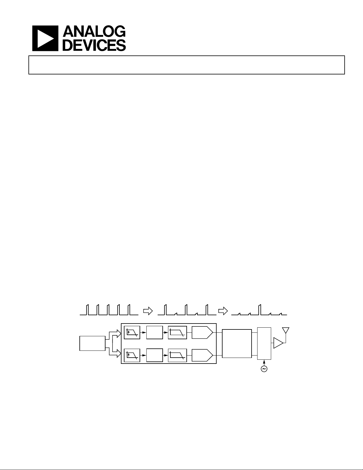
TYPICAL SIGNAL CHAIN
Dual, 16-Bit, 1230 MSPS,
The AD9146 TxDAC+® includes features optimized for direct
conversion transmit applications, including complex digital modulation, and gain and offset compensation. The DAC outputs
are optimized to interface seamlessly with analog quadrature
modulators, such as the ADL537x F-MOD series from Analog
Devices, Inc. A 3-wire serial port interface provides for programming/readback of many internal parameters. Full-scale output
current can be programmed over a range of 8.7 mA to 31.7 mA.
The AD9146 comes in a 48-lead LFCSP.
PRODUCT HIGHLIGHTS
1. Ultralow noise and intermodulation distortion (IMD)
enable high quality synthesis of wideband signals from
baseband to high intermediate frequencies (IF).
2. Proprietary DAC output switching technique enhances
dynamic performance.
3. Current outputs are easily configured for various single-
ended or differential circuit topologies.
4. Compact LVDS digital interface offers reduced width
data bus.
COMPANION PRODUCTS
IQ Modulators: ADL5370, ADL537x family
IQ Modulators with PLL and VCO: ADRF6701, ADRF670x family
Clock Drivers: AD9516, AD951x family
Voltage Regulator Design Tool: ADIsimPower
Additional companion products on the AD9146 product page
Information furnishe d by Analog Devices is be lieved to be accurate and reliable. However, no
responsibility is assumed by Analog Devices for its use, nor for any infringements of patents or other
rights of third parties that may result from its use. Specifications subject to change without notice. No
licen se is granted by implication or otherwise under any patent or patent rights of Analog Devices.
Figure 1.
One Technology Way, P.O. Box 9106, Norwood, MA 02062-9106, U.S.A.
Tel: 781.329.4700
www.analog.com

AD9146 Data Sheet
TABLE OF CONTENTS
Features .............................................................................................. 1
Applications ....................................................................................... 1
General Description ......................................................................... 1
Product Highlights ........................................................................... 1
Companion Products ....................................................................... 1
Typical Signal Chain......................................................................... 1
Revision History ............................................................................... 3
Functional Block Diagram .............................................................. 4
Specifications ..................................................................................... 5
DC Specifications ......................................................................... 5
Digital Specifications ................................................................... 6
Digital Input Data Timing Specifications ................................. 6
AC Specifications .......................................................................... 7
Absolute Maximum Ratings ............................................................ 8
Thermal Resistance ...................................................................... 8
ESD Caution .................................................................................. 8
Pin Configuration and Function Descriptions ............................. 9
Typical Performance Characteristics ........................................... 11
Terminology .................................................................................... 15
Theory of Operation ...................................................................... 16
Serial Port Operation ................................................................. 16
Data Format ................................................................................ 16
Serial Port Pin Descriptions ...................................................... 16
Serial Port Options ..................................................................... 17
Device Configuration Register Map and Descriptions ......... 18
LVDS Input Data Ports .................................................................. 28
Byte Interface Mode ................................................................... 28
Nibble Interface Mode ............................................................... 28
FIFO Operation .......................................................................... 28
Interface Timing ......................................................................... 31
Digital Datapath .............................................................................. 32
Premodulation ............................................................................ 32
Interpolation Filters.................................................................... 32
Datapath Configuration ............................................................ 34
Determining Interpolation Filter Modes ................................ 34
Coarse Modulation Mixing Sequences .................................... 35
Quadrature Phase Correction ................................................... 35
Rev. A | Page 2 of 56
DC Offset Correction ................................................................ 35
Inverse Sinc Filter ....................................................................... 36
DAC Input Clock Configurations ................................................ 37
Driving the DACCLK and REFCLK Inputs ........................... 37
Direct Clocking .......................................................................... 37
Clock Multiplication .................................................................. 37
PLL Settings ................................................................................ 38
Configuring the VCO Tuning Band ........................................ 38
Analog Outputs............................................................................... 39
Transmit DAC Operation .......................................................... 39
Auxiliary DAC Operation ......................................................... 40
Interfacing to Modulators ......................................................... 41
Baseband Filter Implementation .............................................. 41
Driving the ADL5375-15 .......................................................... 41
Reducing LO Leakage and Unwanted Sidebands .................. 42
Device Power Management........................................................... 43
Power Dissipation....................................................................... 43
Tx Enable ..................................................................................... 43
Temperature Sensor ................................................................... 44
Multichip Synchronization ............................................................ 45
Synchronization with Clock Multiplication ............................... 45
Synchronization with Direct Clocking .................................... 46
Data Rate Mode Synchronization ............................................ 46
FIFO Rate Mode Synchronization ........................................... 47
Additional Synchronization Features ...................................... 48
Interrupt Request Operation ........................................................ 49
Interrupt Service Routine .......................................................... 49
Interface Timing Validation .......................................................... 50
SED Operation ............................................................................ 50
SED Example............................................................................... 51
Example Start-Up Routine ............................................................ 52
Device Configuration ................................................................ 52
Derived PLL Settings ................................................................. 52
Start-Up Sequence ...................................................................... 52
Outline Dimensions ....................................................................... 53
Ordering Guide .......................................................................... 53

Data Sheet AD9146
REVISION HISTORY
1/12—Rev. 0 to Rev. A
Change to General Description Section ......................................... 1
Change to DCI Delay[1:0], Table 11 ............................................. 23
Changes to Interface Timing Section, Figure 37, and
Figure 38 ........................................................................................... 31
Changes to SED Operation Section and Table 26 ....................... 50
4/11—Revision 0: Initial Version
Rev. A | Page 3 of 56
AD9146 Data Sheet
MULTICHIP
SYNCHRONIZATION
D7P/D7N
D0P/D0N
DATA
RECEIVER
FIFO HB2
f
DATA
/2
PRE
MOD
HB1_CLK
MODE
HB2_CLK
INTP
FACTOR
PHASE
CORRECTION
INTERNAL CLOCK TIMING AND CONTROL LOGIC
16
16
10
16
16
I OFFSET
Q OFFSET
INV
SINC
AUX
1.2G
DAC 1
16-BIT
IOUT1P
IOUT1N
AUX
1.2G
DAC 2
16-BIT
IOUT2P
IOUT2N
REF
AND
BIAS
FSADJ
DACCLKP
DACCLKN
REFCLKP
REFCLKN
REFIO
10
GAIN 110GAIN 2
DAC_CLK
SERIAL
INPUT/OUTPUT
PORT
PROGRAMMING
REGISTERS
POWER-ON
RESET
SDIO
SCLK
CS
RESET
IRQ
0
1
CLOCK
MULTIPLIER
(2× TO 16×)
CLK
RCVR
CLK
RCVR
PLL CONTROL
SYNC
DAC CLK_SEL
DAC_CLK
PLL_LOCK
DCI
FRAME
INVSINC_CLK
09691-002
HB1
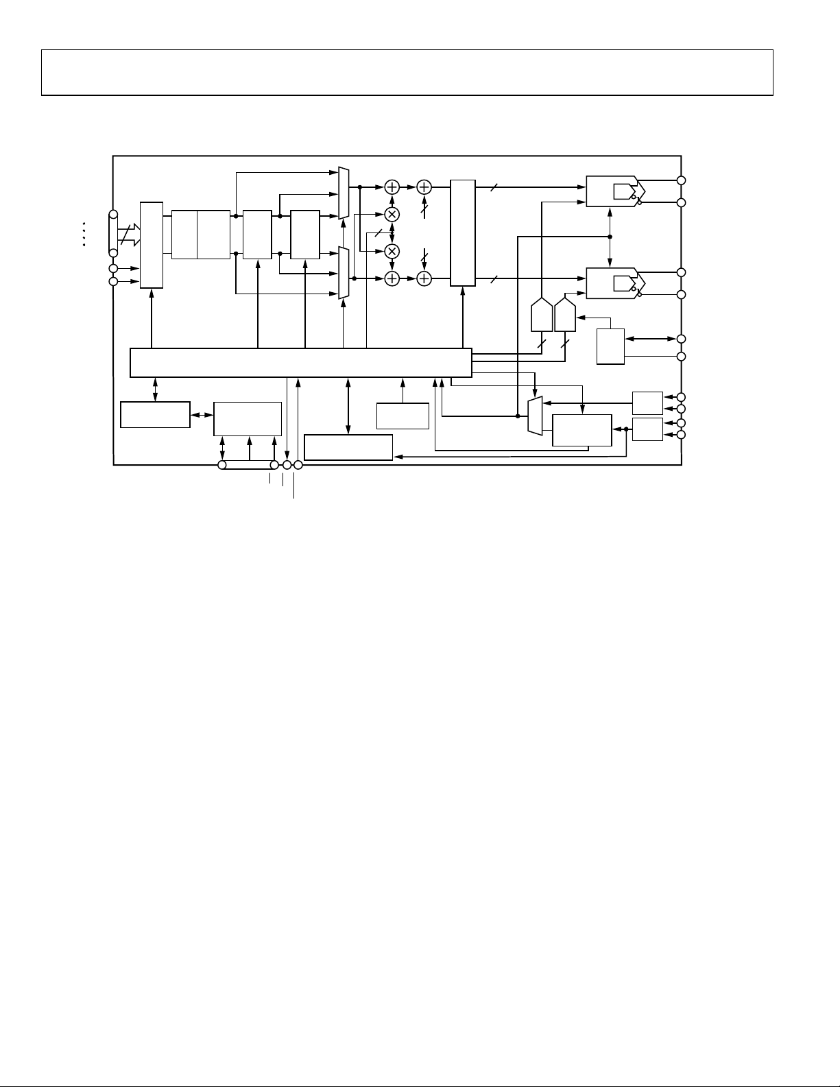
FUNCTIONAL BLOCK DIAGRAM
Figure 2.
Rev. A | Page 4 of 56

Data Sheet AD9146
Power Supply Rejection Ratio, AVDD33
−0.3 +0.3
% FSR/V
CVDD18
1.71
1.8
1.89
V
PLL On
864 mW
SPECIFICATIONS
DC SPECIFICATIONS
T
to T
MIN
Table 1.
Parameter Min Typ Max Unit
RESOLUTION 16 Bits
ACCURACY
Differential Nonlinearity (DNL) ±2.1 LSB
Integral Nonlinearity (INL) ±3.7 LSB
MAIN DAC OUTPUTS
Offset Error −0.001 0 +0.001 % FSR
Gain Error (with Internal Reference) −3.6 ±2 +3.6 % FSR
Full-Scale Output Current1 8.66 19.6 31.66 mA
Output Compliance Range −1.0 +1.0 V
Output Resistance 10 MΩ
Gain DAC Monotonicity Guaranteed
Settling Time to Within ±0.5 LSB 20 ns
MAIN DAC TEMPERATURE DRIFT
Offset 0.04 ppm/°C
Gain 100 ppm/°C
Reference Voltage 30 ppm/°C
REFERENCE
Internal Reference Voltage 1.2 V
Output Resistance 5 kΩ
ANALOG SUPPLY VOLTAGES
AVDD33 3.13 3.3 3.47 V
, AV D D3 3 = 3.3 V, DVDD18 = 1.8 V, CVDD18 = 1.8 V, IFS = 20 mA, maximum sample rate, unless otherwise noted.
MAX
DIGITAL SUPPLY VOLTAGES
DVDD18 1.71 1.8 1.89 V
POWER CONSUMPTION
2× Mode, f
PLL Off 780 mW
AVDD33 56 mA
CVDD18 58 mA
DVDD18 343 mA
Power-Down Mode (Register 0x01 = 0xFC) 8.5 19 mW
POWER-UP TIME 260 ms
OPERATING RANGE −40 +25 +85 °C
1
Based on a 10 kΩ external resistor between FSADJ and AVSS.
= 500 MSPS, IF = 10 MHz
DAC
Rev. A | Page 5 of 56

AD9146 Data Sheet
DIGITAL SPECIFICATIONS
T
to T
MIN
Table 2.
Parameter Test Conditions/Comments Min Typ Max Unit
CMOS INPUT LOGIC LEVEL
Input VIN Logic High 1.2 V
Input VIN Logic Low 0.6 V
CMOS OUTPUT LOGIC LEVEL
Output V
Output V
LVDS RECEIVER INPUTS1 Applies to data, DCI, and FRAME inputs
Input Voltage Range, VIA or VIB 825 1575 mV
Input Differential Threshold, V
Input Differential Hysteresis, V
Receiver Differential Input Impedance, RIN 80 120 Ω
LVDS Input Rate See Table 5
DAC CLOCK INPUT (DACCLKP, DACCLKN)
Differential Peak-to-Peak Voltage 100 500 2000 mV
Common-Mode Voltage Self-biased input, ac-coupled 1.25 V
Maximum Clock Rate 1200 MHz
REFCLK INPUT (REFCLKP, REFCLKN)
Differential Peak-to-Peak Voltage 100 500 2000 mV
Common-Mode Voltage 1.25 V
REFCLK Frequency
SERIAL PORT INTERFACE
Maximum Clock Rate (SCLK) 40 MHz
Minimum Pulse Width High (t
Minimum Pulse Width Low (t
Setup Time, SDIO to SCLK (tDS) 2.09 ns
Hold Time, SDIO to SCLK (tDH) 0.844 ns
Data Valid, SDIO to SCLK (tDV) 2.904 ns
Setup Time, CS to SCLK (t
1
LVDS receiver is compliant with the IEEE 1596 reduced range link, unless otherwise noted.
, AV D D3 3 = 3.3 V, DVDD18 = 1.8 V, CVDD18 = 1.8 V, IFS = 20 mA, maximum sample rate, unless otherwise noted.
MAX
Logic High 1.4 V
OUT
Logic Low 0.4 V
OUT
−100 +100 mV
IDTH
to V
IDTHH
PLL Mode 1 GHz ≤ f
SYNC Mode See the Multichip Synchronization
20 mV
IDTHL
≤ 2.1 GHz 15.625 525 MHz
VCO
0 525 MHz
section for conditions
) 12.5 ns
PWH
) 12.5 ns
PWL
) 2.38 ns
DCSB
DIGITAL INPUT DATA TIMING SPECIFICATIONS
Table 3.
Parameter Value Unit
LATENCY (DACCLK CYCLES)
1× Interpolation (With or Without Modulation) 64 Cycles
2× Interpolation (With or Without Modulation) 135 Cycles
4× Interpolation (With or Without Modulation) 292 Cycles
Inverse Sinc 20 Cycles
Rev. A | Page 6 of 56

Data Sheet AD9146
f
= 800 MSPS, f
= 100 MHz
81 dBc
W-CDMA ADJACENT CHANNEL LEAKAGE RATIO (ACLR), SINGLE-CARRIER
2× (HB1)
1200
1230
150
153.75
300
307.5
AC SPECIFICATIONS
T
to T
MIN
Table 4.
Parameter Min Typ Max Unit
SPURIOUS-FREE DYNAMIC RANGE (SFDR)
f
DAC
f
DAC
f
DAC
TWO-TONE INTERMODULATION DISTORTION (IMD)
f
DAC
f
DAC
f
DAC
DAC
NOISE SPECTRAL DENSITY (NSD), SINGLE-CARRIER W-CDMA
f
DAC
f
DAC
W-CDMA ADJACENT CHANNEL LEAKAGE RATIO (ACLR), FOUR-CARRIER
f
DAC
f
DAC
f
DAC
, AV D D3 3 = 3.3 V, DVDD18 = 1.8 V, CVDD18 = 1.8 V, IFS = 20 mA, maximum sample rate, unless otherwise noted.
MAX
= 200 MSPS, f
= 400 MSPS, f
= 800 MSPS, f
= 600 MSPS, f
= 600 MSPS, f
= 800 MSPS, f
= 400 MSPS, f
= 800 MSPS, f
= 491.52 MSPS, f
= 983.04 MSPS, f
= 983.04 MSPS, f
= 50 MHz 70 dBc
OUT
= 70 MHz 65 dBc
OUT
= 70 MHz 67 dBc
OUT
= 50 MHz 85 dBc
OUT
= 80 MHz 82 dBc
OUT
= 60 MHz 83 dBc
OUT
OUT
= 80 MHz −162 dBm/Hz
OUT
= 80 MHz −164 dBm/Hz
OUT
= 15 MHz 75 dBc
OUT
= 80 MHz 77 dBc
OUT
= 200 MHz 76 dBc
OUT
f
= 983.04 MSPS, f
DAC
f
= 983.04 MSPS, f
DAC
= 80 MHz 82 dBc
OUT
= 122.88 MHz 80 dBc
OUT
Table 5. Maximum Rate (MSPS) with DVDD and CVDD Supply Regulation
Interface
Mode
Interpolation
Factor
f
1.8 V ± 5% 1.9 V ± 5% 1.8 V ± 5% 1.9 V ± 5% 1.8 V ± 5% 1.9 V ± 5% 1.8 V ± 5% 1.9 V ± 5%
(MSPS) f
IN TER FACE
(MSPS) f
HB1
(MSPS) f
HB2
(MSPS)
DAC
Byte (8 Bits) 1× 1200 1230 300 307.5
2× (HB1) 1200 1230 300 307.5 600 615
2× (HB2) 1200 1230 300 307.5 600 615
4× 1200 1230 300 307.5 600 615 1200 1230
Nibble (4 Bits) 1× 1200 1230 150 153.75
2× (HB2) 1200 1230 150 153.75 300 307.5
4× 1200 1230 150 153.75 300 307.5 600 615
Rev. A | Page 7 of 56
AD9146 Data Sheet
DVDD18, CVDD18 to AVSS, EPAD,
−0.3 V to +2.1 V
, SCLK, SDIO to EPAD
−0.3 V to DVDD18 + 0.3 V
ABSOLUTE MAXIMUM RATINGS
Table 6.
Parameter Rating
AVDD33 to AVSS, EPAD, CVSS −0.3 V to +3.6 V
CVSS
AVSS to EPAD, CVSS −0.3 V to +0.3 V
EPAD to AVSS, CVSS −0.3 V to +0.3 V
CVSS to AVSS, EPAD −0.3 V to +0.3 V
FSADJ, REFIO, IOUT1P, IOUT1N,
IOUT2P, IOUT2N to AVSS
D[7:0]P, D[7:0]N, FRAMEP, FRAMEN,
DCIP, DCIN to EPAD
DACCLKP, DACCLKN, REFCLKP,
REFCLKN to EPAD
RESET, IRQ, CS
Junction Temperature 125°C
Storage Temperature Range −65°C to +150°C
−0.3 V to AVDD33 + 0.3 V
−0.3 V to DVDD18 + 0.3 V
−0.3 V to CVDD18 + 0.3 V
Stresses above those listed under Absolute Maximum Ratings
may cause permanent damage to the device. This is a stress
rating only; functional operation of the device at these or any
other conditions above those indicated in the operational
section of this specification is not implied. Exposure to absolute
maximum rating conditions for extended periods may affect
device reliability.
THERMAL RESISTANCE
The exposed pad (EPAD) of the 48-lead LFCSP must be soldered
to the ground plane (AVSS). The EPAD provides an electrical,
thermal, and mechanical connection to the board.
Typical θ
, θJB, and θJC values are specified for a 4-layer board and
JA
an 8-layer board in still air. Airflow increases heat dissipation,
effectively reducing θ
and θJB.
JA
Table 7. Thermal Resistance
Package1 PCB θJA θJB θJC Unit
48-Lead LFCSP 4-layer 23.2 8.5 8.7 °C/W
48-Lead LFCSP 8-layer 16.4 3.9 7.1 °C/W
1
EPAD soldered to ground plane.
ESD CAUTION
Rev. A | Page 8 of 56
Data Sheet AD9146
NOTES
1. THE EXP OSED PAD (EPAD) M US T BE SOLDERE D TO THE GROUND PLANE
(AVSS). THE EPAD PROVIDES AN ELECT RICAL, THERM AL, AND
MECHANICAL CO NNE CTION TO THE BOARD.
DACCLKP
DACCLKN
AD9146
TOP VIEW
(Not to S cale)
PIN 1
INDICATOR
09691-003
2
CVDD18
1.8 V Clock Supply. Supplies clock receivers, clock distribution, and PLL circuitry.
7
REFCLKN
PLL Reference Clock Input, Negative. This pin has a secondary function as a synchronization input.
23
D2P
Data Bit 2, Positive.
24
D2N
Data Bit 2, Negative.
PIN CONFIGURATION AND FUNCTION DESCRIPTIONS
AVDD33
IOUT1P
IOUT1N
AVDD33
AVSS
FSADJ
REFIO
AVSS
AVDD33
IOUT2N
IOUT2P
4847464544434241403938
AVDD33
37
D2N
RESET36
DVDD18
35
IRQ
34
CS
33
SCLK
32
SDIO
31
TXENABLE
30
DVDD18
29
D0N
28
D0P
27
D1N
26
D1P
25
CVDD18
CVDD18
CVSS
REFCLKP
REFCLKN
DVDD18
D7P
D7N
D6P
D6N
1
2
3
4
5
6
7
8
9
10
11
12
13141516171819
D5P
D4P
D4N
D5N
DCIP
DCIN
FRAMEP
2021222324
D3P
D2P
D3N
FRAMEN
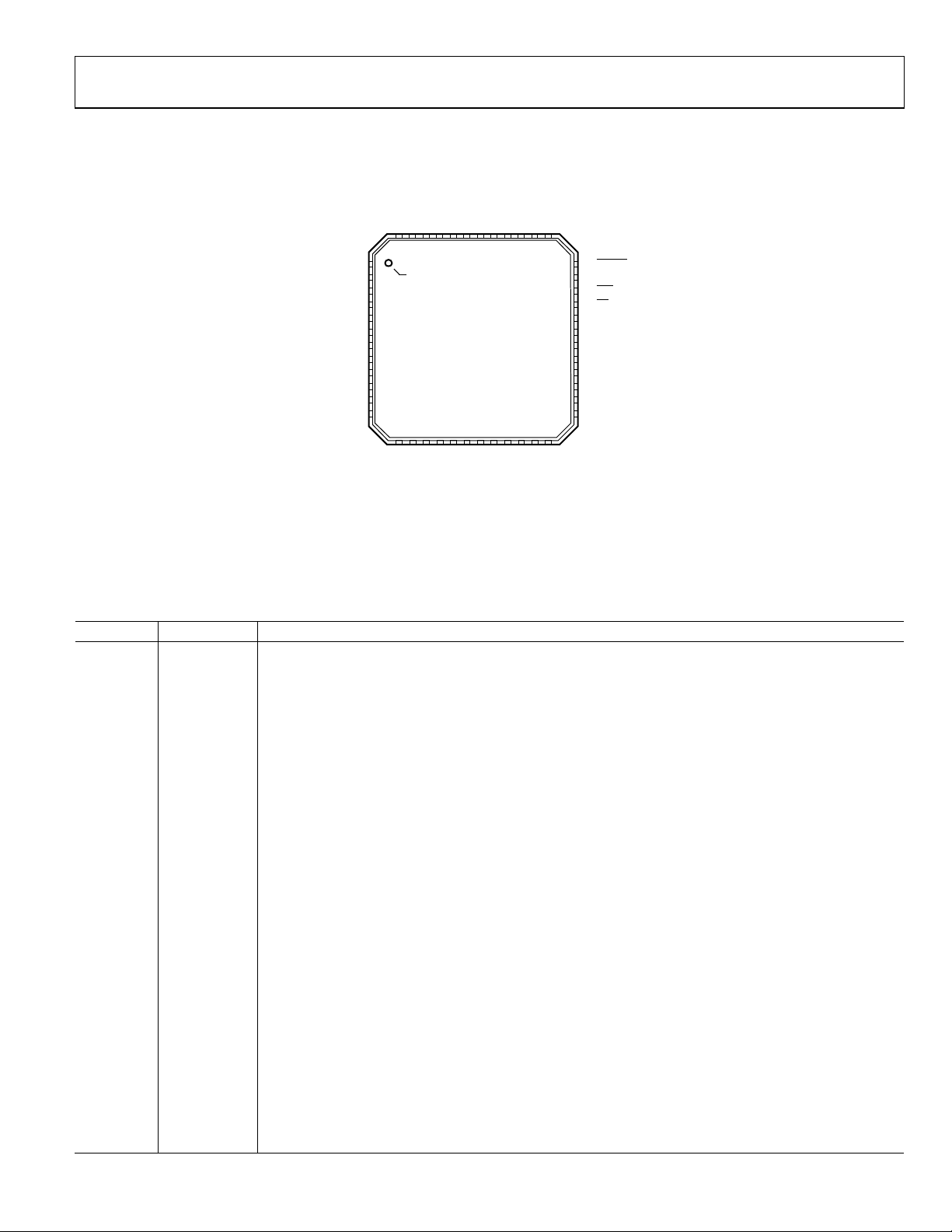
Figure 3. Pin Configuration
Table 8. Pin Function Descriptions
Pin No. Mnemonic Description
1 CVDD18 1.8 V Clock Supply. Supplies clock receivers, clock distribution, and PLL circuitry.
3 DACCLKP DAC Clock Input, Positive.
4 DACCLKN DAC Clock Input, Negative.
5 CVSS Clock Supply Common.
6 REFCLKP PLL Reference Clock Input, Positive. This pin has a secondary function as a synchronization input.
8 DVDD18 1.8 V Digital Supply. Supplies power to digital core and digital data ports.
9 D7P Data Bit 7 (MSB), Positive.
10 D7N Data Bit 7 (MSB), Negative.
11 D6P Data Bit 6, Positive.
12 D6N Data Bit 6, Negative.
13 D5P Data Bit 5, Positive.
14 D5N Data Bit 5, Negative.
15 D4P Data Bit 4, Positive.
16 D4N Data Bit 4, Negative.
17 DCIP Data Clock Input, Positive.
18 DCIN Data Clock Input, Negative.
19 FRAMEP Frame Input, Positive.
20 FRAMEN Frame Input, Negative.
21 D3P Data Bit 3, Positive.
22 D3N Data Bit 3, Negative.
25 D1P Data Bit 1, Positive.
26 D1N Data Bit 1, Negative.
27 D0P Data Bit 0 (LSB), Positive.
Rev. A | Page 9 of 56

AD9146 Data Sheet
32
SCLK
Serial Port Clock Input (CMOS).
48
AVDD33
3.3 V Analog Supply.
EPAD
The exposed pad (EPAD) must be soldered to the ground plane (AVSS). The EPAD provides an electrical,
Pin No. Mnemonic Description
28 D0N Data Bit 0 (LSB), Negative.
29 DVDD18 1.8 V Digital Supply. Supplies power to digital core and digital data ports.
30 TXENABLE Active High Transmit Path Enable (CMOS). A low level on this pin clamps the DAC outputs to midscale.
31 SDIO Serial Port Data Input/Output (CMOS).
33
34
35 DVDD18 1.8 V Digital Supply. Supplies power to digital core and digital data ports.
36
37 AVDD33 3.3 V Analog Supply.
38 IOUT2P Q DAC Positive Current Output.
39 IOUT2N Q DAC Negative Current Output.
40 AVDD33 3.3 V Analog Supply.
41 AVS S Analog Supply Common.
42 REFIO 1.2 V Band Gap Voltage Reference Output. Should be decoupled to AVSS with a 0.1 µF capacitor.
43 FSADJ Full-Scale Current Output Adjust. Place a 10 kΩ resistor from this pin to AVSS.
44 AVS S Analog Supply Common.
45 AVDD33 3.3 V Analog Supply.
46 IOUT1N I DAC Negative Current Output.
47 IOUT1P I DAC Positive Current Output.
Serial Port Chip Select, Active Low (CMOS).
CS
Interrupt Request. Open-drain, active low output. Pull this pin high external to the device.
IRQ
Reset, Active Low (CMOS).
RESET
thermal, and mechanical connection to the board.
Rev. A | Page 10 of 56
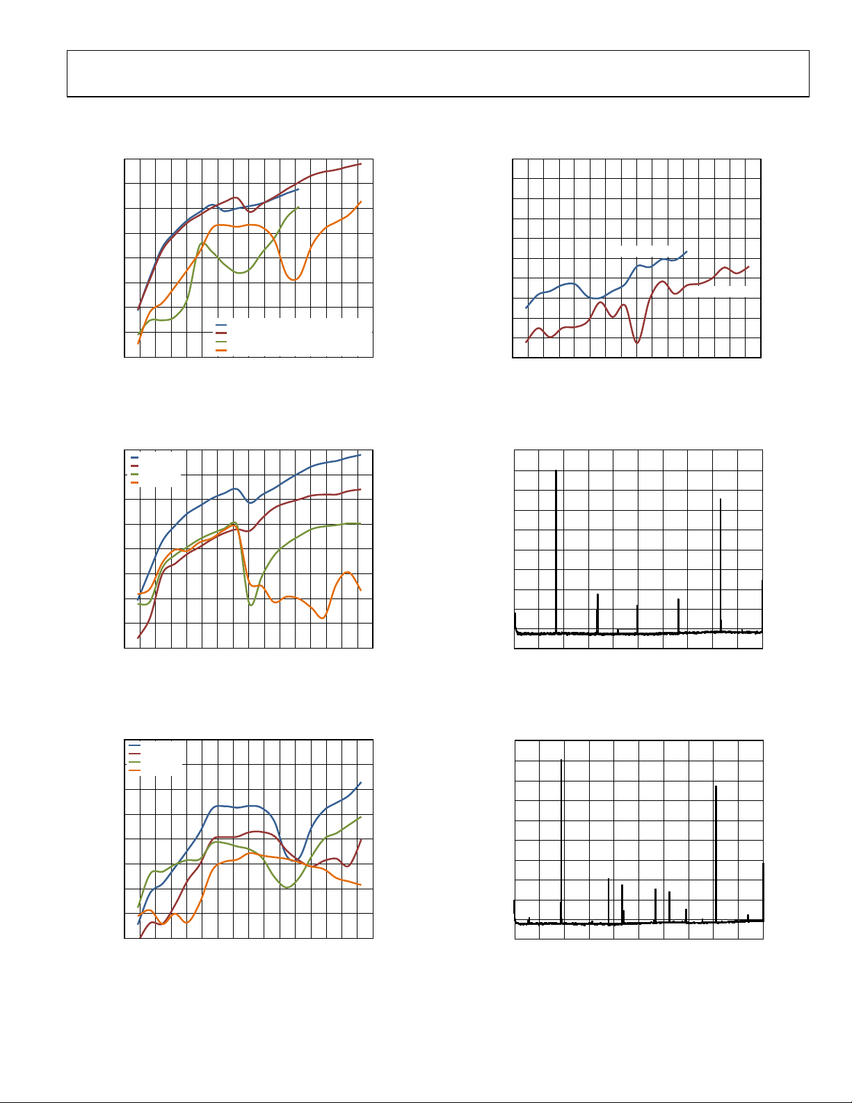
Data Sheet AD9146
–90
–85
–80
–75
–70
–65
–60
–55
–50
0 50 100 150 200 250 300 350 400
HARMONICS (dBc)
f
OUT
(MHz)
2×, 300MSPS, S E COND HARMONIC
4×, 200MSPS, S E COND HARMONIC
2×, 300MSPS, THIRD HARMONI C
4×, 200MSPS, THIRD HARMONI C
09691-076
–90
–85
–80
–75
–70
–65
–60
–55
–50
0 50 100 150 200 250 300 350 400
SECOND HARMONIC (dBc)
f
OUT
(MHz)
0dBFS
–6dBFS
–12dBFS
–18dBFS
09691-077
–90
–85
–80
–75
–70
–65
–60
–55
–50
0 50 100 150 200 250 300 350 400
THIRD HARMONIC (dBc)
f
OUT
(MHz)
0dBFS
–6dBFS
–12dBFS
–18dBFS
09691-078
f
OUT
(MHz)
–80
–78
–76
–74
–72
–70
–68
–66
–64
–62
–60
0 50 100 150 200 250 300 350 400
HIGHEST DIGITAL SPUR (dBc)
09691-079
2×, 300MSPS
4×, 200MSPS
10
0
–10
–20
–30
–40
–50
–60
–70
–80
–90
START 1MHz
#RES BW 10kHz
STOP 600MHz
SWEEP 7.22s (1001pts)
VBW 10kHz
09691-089
AMPLIT UDE ( dBm)
10
0
–10
–20
AMPLIT UDE ( dBm)
–30
–40
–50
–60
–70
–80
–90
START 1MHz
#RES BW 10kHz
STOP 800MHz
SWEEP 9.63s (1001pts)VBW 10kHz
09691-090
TYPICAL PERFORMANCE CHARACTERISTICS
Figure 4. Harmonics vs. f
Digital Scale = 0 dBFS, I
Figure 5. Second Harmonic vs. f
f
= 400 MSPS, IFS = 20 mA
DATA
over f
OUT
over Digital Scale, 4× Interpolation,
OUT
and Interpolation,
DATA
= 20 mA
FS
Figure 7. Highest Digital Spur vs. f
Digital Scale = 0 dBFS, I
OUT
over f
FS
Figure 8. Single-Tone Spectrum, 2× Interpolation,
f
= 300 MSPS, f
DATA
= 101 MHz
OUT
and Interpolation,
DATA
= 20 mA
Figure 6. Third Harmonic vs. f
f
OUT
= 400 MSPS, IFS = 20 mA
DATA
over Digital Scale, 4× Interpolation,
Rev. A | Page 11 of 56
Figure 9. Single-Tone Spectrum, 4× Interpolation,
f
= 200 MSPS, f
DATA
= 151 MHz
OUT
AD9146 Data Sheet
–95
–90
–85
–80
–75
–70
–65
–60
–55
0 50 100 150 200 250 300 350 400
IMD (dBc)
f
OUT
(MHz)
2×, 300MSPS
4×, 200MSPS
09691-080
–95
–90
–85
–80
–75
–70
–65
–60
–55
0 50 100 150 200 250 300 350 400
IMD (dBc)
0dBFS
–6dBFS
–12dBFS
–18dBFS
09691-081
f
OUT
(MHz)
–90
–85
–80
–75
–70
–65
–60
–55
–50
0 50 100 150 200 250 300 350 400
IMD (dBc)
f
OUT
(MHz)
IFS = 10mA
I
FS
= 20mA
I
FS
= 30mA
09691-082
–95
–90
–85
–80
–75
–70
–65
–60
–55
–50
–45
0 50 100 150 200 250 300 350 400
IMD (dBc)
f
OUT
(MHz)
PLL ON
09691-083
PLL OFF
0 50 100 150 200 250 300 350 400
NSD (dBm/Hz)
f
OUT
(MHz)
–170
–165
–160
–155
–150
–145
–140
–135
–130
SINGLE-TONE: 2×, 200M S P S
SINGLE-T
ONE: 4×, 200MS P S
W-CDMA: 2×, 200MSPS
W-CDMA: 4×, 200MSPS
09691-084
–170
–165
–160
–155
–150
–145
–140
–135
–130
0 50 100 150 200 250 300 350 400
NSD (dBm/Hz)
f
OUT
(MHz)
SINGLE-TONE: 2×, 200M S P S
SINGLE-TONE: 4×, 200M S P S
W-CDMA: 2×, 200MSPS
W-CDMA: 4×, 200MSPS
09691-085
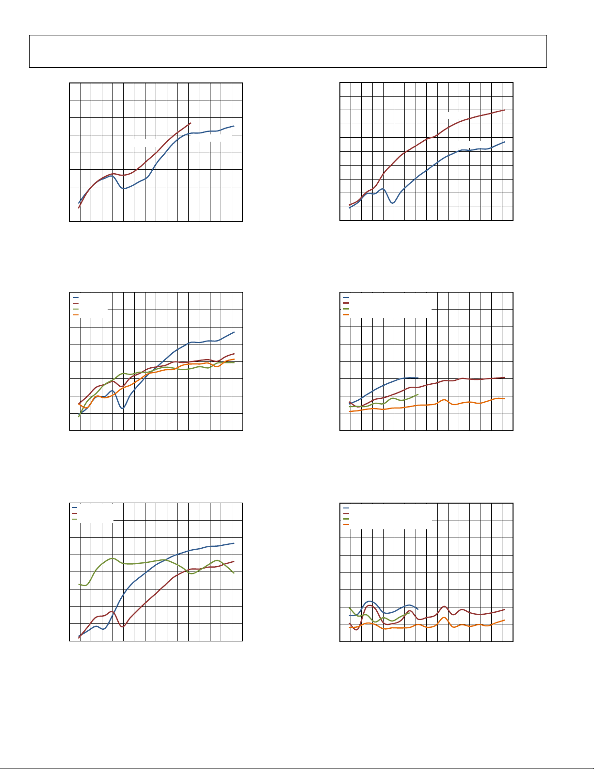
Figure 10. IMD vs. f
Digital Scale = 0 dBFS, I
Figure 11. IMD vs. f
f
DATA
over f
OUT
over Digital Scale, 4× Interpolation,
OUT
and Interpolation,
DATA
= 20 mA
FS
= 400 MSPS, IFS = 20 mA
Figure 13. IMD vs. f
Digital Scale = 0 dBFS, I
, 4× Interpolation, f
OUT
= 20 mA, PLL On and PLL Off
FS
= 200 MSPS,
DATA
Figure 14. NSD vs. f
f
DATA
over Interpolation, Single-Tone and W-CDMA Signals,
OUT
= 200 MSPS, Digital Scale = 0 dBFS, IFS = 20 mA, PLL Off
Figure 12. IMD vs. f
f
DATA
over Full-Scale Current, 4× Interpolation,
OUT
= 400 MSPS, Digital Scale = 0 dBFS
Figure 15. NSD vs. f
f
DATA
over Interpolation, Single-Tone and W-CDMA Signals,
OUT
= 200 MSPS, Digital Scale = 0 dBFS, IFS = 20 mA, PLL On
Rev. A | Page 12 of 56
Data Sheet AD9146
–80
–78
–76
–74
–72
–70
–68
–66
–64
–62
–60
0 40 80 120 160 200 240 280 320 360 400 440 480
ACLR (dBc)
0dBFS
–3dBFS
–6dBFS
f
OUT
(MHz)
09691-093
0 40 80 120 160 200 240 280 320 360 400 440 480
ACLR (dBc)
0dBFS
–3dBFS
–6dBFS
–80
–78
–76
–74
–72
–70
–68
–66
–64
–62
–60
f
OUT
(MHz)
09691-094
0 40 80 120 160 200 240 280 320 360 400 440 480
ACLR (dBc)
0dBFS
–3dBFS
–6dBFS
–80
–78
–76
–74
–72
–70
–68
–66
–64
–62
–60
f
OUT
(MHz)
09691-086
0 40 80 120 160 200 240 280 320 360 400 440 480
ACLR (dBc)
2×, PLL OFF
2×, PLL ON
4×, PLL OFF
4×, PLL ON
–80
–78
–76
–74
–72
–70
–68
–66
–64
–62
–60
f
OUT
(MHz)
09691-095
–80
–78
–76
–74
–72
–70
–68
–66
–64
–62
–60
0 40 80 120 160 200 240 280 320 360 400 440 480
ACLR (dBc)
2×, PLL OFF
2×, PLL ON
4×, PLL OFF
4×, PLL ON
f
OUT
(MHz)
09691-096
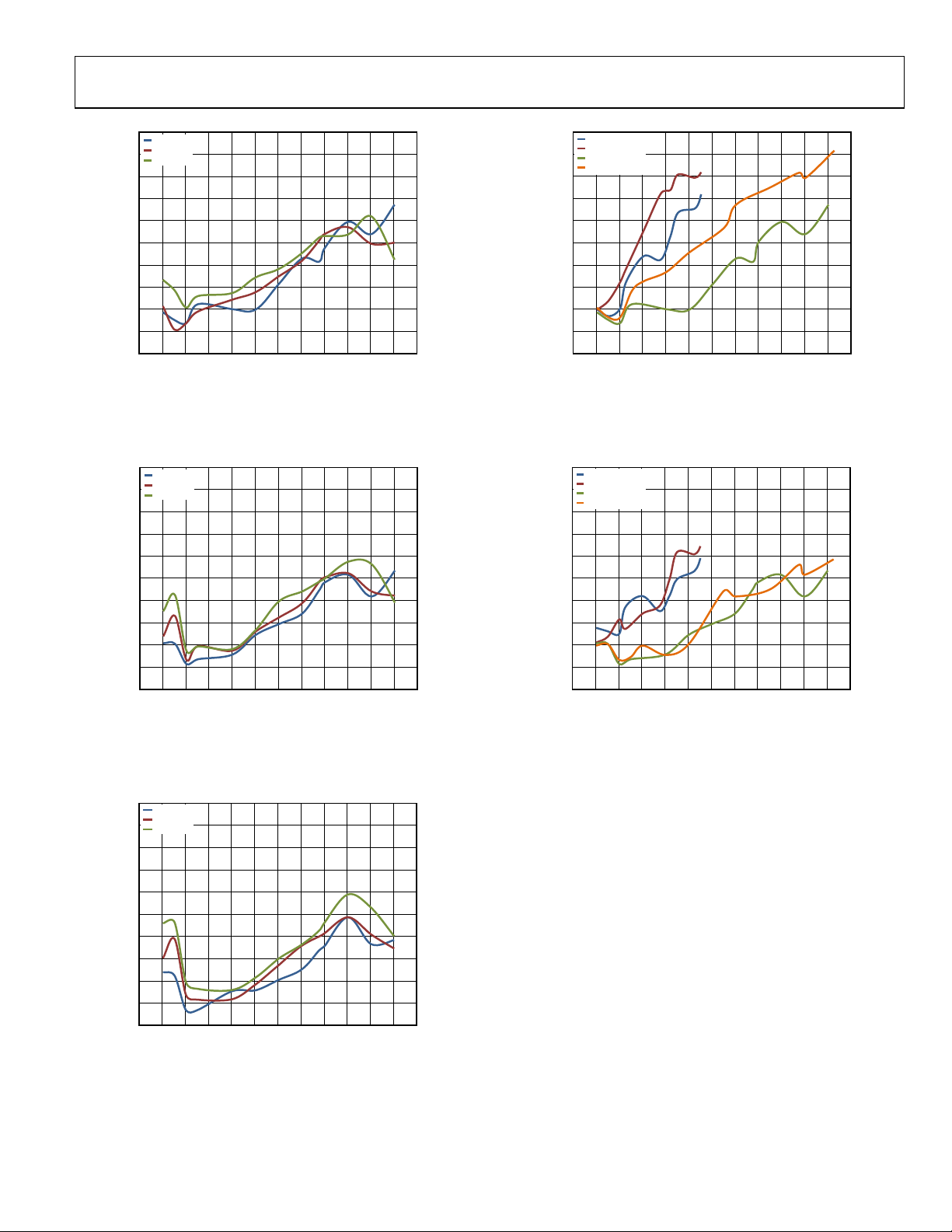
Figure 16. Four-Carrier W-CDMA ACLR vs. f
Channel, 4× Int erpolation, f
DATA
Figure 17. Four-Carrier W-CDMA ACLR vs. f
Alternate Channel, 4× Interpolation, f
over Digital Scale, Adjacent
OUT
= 245.76 MSPS, PLL Off
over Digital Scale, First
OUT
= 245.76 MSPS, PLL Off
DATA
Figure 19. Four-Carrier W-CDMA ACLR vs. f
Channel, f
= 245.76 MSPS, PLL Off and PLL On
DATA
Figure 20. Four-Carrier W-CDMA ACLR vs. f
Alternate Channel, f
= 245.76 MSPS, PLL Off and PLL On
DATA
over Interpolation, Adjacent
OUT
over Interpolation, First
OUT
Figure 18. Four-Carrier W-CDMA ACLR vs. f
Alternate Channel, 4× Interpolation, f
over Digital Scale, Second
OUT
= 245.76 MSPS, PLL Off
DATA
Rev. A | Page 13 of 56
AD9146 Data Sheet
–80
–78
–76
–74
–72
–70
–68
–66
–64
–62
–60
0 40 80 120 160 200 240 280 320 360 400 440 480
ACLR (dBc)
f
OUT
(MHz)
2×, PLL OFF
2×, PL
L ON
4×, PLL OFF
4×, PLL ON
09691-087
AMPLIT UDE ( dBm)
CENTER 122MHz
#RES BW 30kHz
SPAN 49.68MHz
SWEEP 1.371sVBW 3kHz
–35
–25
–55
–45
–75
–65
–95
–105
–125
–115
–85
OFFSET
FREQFILTER
CARRIER
POWER
INTEG
BW dBc
LOWER
ACP-IBWTOTAL CARRIER POWER –16.469dBm/15.36MHz
UPPER
dBm dBc
dBm FILTER
5MHz
10MHz
15MHz
ON1 –22.205dBm/3.84MHz 3.84MHz
3.84MHz
3.84MHz
–76.37
–77.45
–77.59
–98.78
–99.85
–99.99
–77.11
–77.49
–77.51
–99.52
–99.89
–99.91
ON
ON
ON
–22.2dBm –22.4dBm –22.7dBm –22.7dBm
09691-092
–84
–82
–80
–78
–76
–74
–72
–70
–68
–66
–64
–62
–60
0 40 80 120 160 200 240 280 320 360 400 440 480
ACLR (dBc)
f
OUT
(MHz)
1 CARRIER
4 CARRIER
09691-088
CENTER 200MHz
#RES BW 30kHz
SPAN 49.68MHz
SWEEP 1.371sVBW 3kHz
–35
–25
–55
–45
–75
–65
AMPLIT UDE ( dBm)
–95
–105
–125
–115
–85
–23.3dBm –22.9dBm –22.6dBm –22.8dBm
OFFSET
FREQFILTER
CARRIER
POWER
INTEG
BW dBc
LOWER
ACP-IBWTOTAL CARRIER POWER –16.873dBm/15.36MHz
UPPER
dBm dBc dBm FILTER
5MHz
10MHz
15MHz
ON1 –23.284dBm/3.84MHz 3.84MHz
3.84MHz
3.84MHz
–76.55
–76.73
–76.64
–99.49
–99.67
–99.59
–75.66
–75.68
–75.88
–98.60
–98.62
–98.83
ON
ON
ON
09691-091
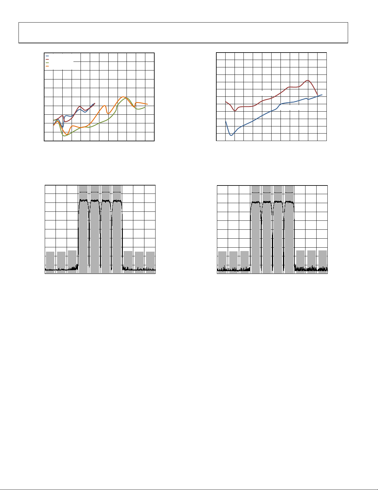
Figure 21. Four-Carrier W-CDMA ACLR vs. f
Alternate Channel, f
= 245.76 MSPS, PLL Off and PLL On
DATA
over Interpolation, Second
OUT
Figure 22. Four-Carrier W-CDMA Performance, 4× Interpolation,
f
= 245.76 MSPS, Digital Scale = −6 dBFS, f
DATA
OUT
= 122 MHz
Figure 23. W-CDMA ACLR vs. f
4× Interpolation, f
DATA
over Number of Carriers, Adjacent Channel,
OUT
= 245.76 MSPS, Digital Scale = −6 dBFS, PLL Off
Figure 24. Four-Carrier W-CDMA Performance, 4× Interpolation,
f
= 245.76 MSPS, Digital Scale = −6 dBFS, f
DATA
OUT
= 200 MHz
Rev. A | Page 14 of 56

Data Sheet AD9146
TERMINOLOGY
Integral Nonlinearity (INL)
INL is the maximum deviation of the actual analog output from
the ideal output, determined by a straight line drawn from zero
scale to full scale.
Differential Nonlinearity (DNL)
DNL is the measure of the variation in analog value, normalized
to full scale, associated with a 1 LSB change in digital input code.
Offset Error
Offset error is the deviation of the output current from the ideal
of 0 mA. For IOUT1P, 0 mA output is expected when all inputs
are set to 0. For IOUT1N, 0 mA output is expected when all
inputs are set to 1.
Gain Error
Gain error is the difference between the actual and ideal output
span. The actual span is determined by the difference between
the output when all inputs are set to 1 and the output when all
inputs are set to 0.
Output Compliance Range
The output compliance range is the range of allowable voltage
at the output of a current output DAC. Operation beyond the
maximum compliance limits can cause either output stage
saturation or breakdown, resulting in nonlinear performance.
Temperature Drift
Temperature drift is specified as the maximum change from
the ambient (25°C) value to the value at either T
MIN
or T
MAX
.
For offset and gain drift, the drift is reported in ppm of full-scale
range (FSR) per degree Celsius. For reference voltage drift, the
drift is reported in ppm per degree Celsius.
Power Supply Rejection (PSR)
PSR is the maximum change in the full-scale output as the
supplies are varied from minimum to maximum specified
voltages.
Settling Time
Settling time is the time required for the output to reach and
remain within a specified error band around its final value,
measured from the start of the output transition.
Spurious-Free Dynamic Range (SFDR)
SFDR is the difference, in decibels, between the peak amplitude
of the output signal and the peak spurious signal within the dc
to Nyquist frequency of the DAC. Typically, energy in this band
is rejected by the interpolation filters. This specification, therefore, defines how well the interpolation filters work and the
effect of other parasitic coupling paths on the DAC output.
Signal-to-Noise Ratio (SNR)
SNR is the ratio of the rms value of the measured output signal
to the rms sum of all other spectral components below the Nyquist
frequency, excluding the first six harmonics and dc. The value
for SNR is expressed in decibels.
Interpolation Filter
If the digital inputs to the DAC are sampled at a multiple rate of
f
(interpolation rate), a digital filter can be constructed that
DATA
has a sharp transition band near f
appear around f
(output data rate) can be greatly suppressed.
DAC
/2. Images that typically
DATA
Adjacent Channel Leakage Ratio (ACLR)
ACLR is the ratio in decibels relative to the carrier (dBc) between
the measured power within a channel and that of its adjacent
channel.
Complex Image Rejection
In a traditional two-part upconversion, two images are created
around the second IF frequency. These images have the effect
of wasting transmitter power and system bandwidth. By placing
the real part of a second complex modulator in series with the
first complex modulator, either the upper or lower frequency
image near the second IF can be rejected.
Rev. A | Page 15 of 56

32
SCLK
31
SDIO
33
CS
SPI
PORT
09691-032
AD9146 Data Sheet
THEORY OF OPERATION
High performance, small size, and low power consumption
make the AD9146 a very attractive DAC for wired and wireless
communications systems. The dual digital signal path and dual
DAC structure allow an easy interface to common quadrature
modulators when designing single sideband (SSB) transmitters.
The AD9146 offers features that allow simplified synchronization with incoming data and between multiple devices. Auxiliary
DACs are also provided on chip. The auxiliary DACs can be used
for output dc offset compensation (for LO compensation in SSB
transmitters) and for gain matching (for image rejection optimization in SSB transmitters).
SERIAL PORT OPERATION
The serial port is a flexible, synchronous serial communications
port that allows easy interfacing to many industry-standard
microcontrollers and microprocessors. The serial I/O is compatible with most synchronous transfer formats, including both
the Motorola SPI and Intel® SSR protocols. The interface allows
read/write access to all registers that configure the AD9146.
Single-byte or multiple-byte transfers are supported, as well
as MSB first or LSB first transfer formats.
Figure 25. Serial Port Interface Pins
A communication cycle with the AD9146 has two phases.
Phase 1 is the instruction cycle (the writing of an instruction
byte into the device), coincident with the first eight SCLK rising
edges. The instruction byte provides the serial port controller
with information regarding the data transfer cycle—Phase 2 of
the communication cycle. The Phase 1 instruction byte defines
whether the upcoming data transfer is a read or write, along with
the starting register address for the first byte of the data transfer.
The first eight SCLK rising edges of each communication cycle
are used to write the instruction byte into the device.
A logic high on the
CS
pin followed by a logic low resets the
serial port timing to the initial state of the instruction cycle.
From this state, the next eight rising SCLK edges represent the
instruction bits of the current I/O operation.
The remaining SCLK edges are for Phase 2 of the communication
cycle. Phase 2 is the actual data transfer between the device and
the system controller. Phase 2 of the communication cycle is a
transfer of one or more data bytes. Registers change immediately
upon writing to the last bit of each transfer byte.
Rev. A | Page 16 of 56
DATA FORMAT
The instruction byte contains the information shown in Ta ble 9.
Table 9. Serial Port Instruction Byte
I7 (MSB) I6 I5 I4 I3 I2 I1 I0 (LSB)
R/W A6 A5 A4 A3 A2 A1 A0
R/W, Bit 7 of the instruction byte, determines whether a read
or a write data transfer occurs after the instruction byte write.
Logic 1 indicates a read operation, and Logic 0 indicates a write
operation.
A6 to A0, Bit 6 to Bit 0 of the instruction byte, determine the
register that is accessed during the data transfer portion of the
communication cycle. For multibyte transfers, A6 is the starting
byte address. The remaining register addresses are generated by
the device based on the LSB_FIRST bit (Register 0x00, Bit 6).
SERIAL PORT PIN DESCRIPTIONS
Serial Clock (SCLK)
The serial clock pin synchronizes data to and from the device and
runs the internal state machines. The maximum frequency of
SCLK is 40 MHz. All data input is registered on the rising edge
of SCLK. All data is driven out on the falling edge of SCLK.
Chip Select (CS)
An active low input starts and gates a communication cycle.
It allows more than one device to be used on the same serial
communications lines. When the
goes to a high impedance state. During the communication
CS
cycle, the
pin should stay low.
Serial Data I/O (SDIO)
The SDIO pin is a bidirectional pin that functions as an input in
write mode and as an output in read mode. Data is written into
the device on this pin and read from the device on this pin. The
configuration of the SDIO pin is controlled by Register 0x00,
Bit 7. To enable readback of the register data, this bit must be
set to 1.
CS
pin is high, the SDIO pin
Data Sheet AD9146
R/W A6 A5 A4 A3 A2 A1 A0 D7
ND6N
D5
N
D00D10D2
0D30
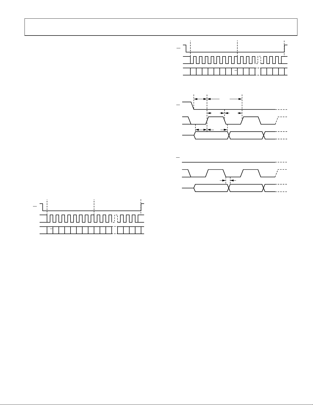
INSTRUCTION CYCLE DATA TRANSFER CYCLE
SCLK
SDIO
09691-033
CS
SCLK
SDIO
CS
A0 A1 A2 A3 A4 A5 A6 R/W D0
0
D1
0
D2
0
D7
ND6N
D5
ND4N
INSTRUCTION CYCLE DATA TRANSFER CYCLE
09691-034
SCLK
SDIO
CS
INSTRUCTION BIT 6INSTRUCTION BIT 7
t
DCSB
t
DS
t
DH
t
PWH
t
PWL
t
SCLK
09691-035
SCLK
SDIO
CS
DATABIT n – 1DATA BIT n
t
DV
09691-036
SERIAL PORT OPTIONS
The serial port can support both MSB first and LSB first data
formats. This functionality is controlled by the LSB_FIRST bit
(Register 0x00, Bit 6). The default is MSB first (LSB_FIRST = 0).
When LSB_FIRST = 0 (MSB first), the instruction and data bits
must be written from MSB to LSB. Multibyte data transfers in
MSB first format start with an instruction byte that includes the
register address of the most significant data byte. Subsequent data
bytes should follow from high address to low address. In MSB first
mode, the serial port internal byte address generator decrements
for each data byte of the multibyte communication cycle.
When LSB_FIRST = 1 (LSB first), the instruction and data bits
must be written from LSB to MSB. Multibyte data transfers in
LSB first format start with an instruction byte that includes the
register address of the least significant data byte. Subsequent data
bytes should follow from low address to high address. In LSB first
mode, the serial port internal byte address generator increments
for each data byte of the multibyte communication cycle.
If the MSB first mode is active, the serial port controller data
address decrements from the data address written toward 0x00
for multibyte I/O operations. If the LSB first mode is active, the
serial port controller data address increments from the data
address written toward 0x7F for multibyte I/O operations.
Figure 27. Serial Port Interface Timing, LSB First
Figure 28. Timing Diagram for Serial Port Register Write
Figure 29. Timing Diagram for Serial Port Register Read
Figure 26. Serial Port Interface Timing, MSB First
Rev. A | Page 17 of 56
 Loading...