Analog Devices AD9057 Datasheet

8-Bit
a
40 MSPS/60 MSPS/80 MSPS A/D Converter
FEATURES
8-Bit, Low Power ADC: 200 mW Typical
120 MHz Analog Bandwidth
On-Chip +2.5 V Reference and T/H
1 V p-p Analog Input Range
Single +5 V Supply Operation
+5 V or +3 V Logic Interface
Power-Down Mode: < 10 mW
Three Performance Grades (40 MSPS, 60 MSPS, 80 MSPS)
APPLICATIONS
Digital Communications (QAM Demodulators)
RGB & YC/Composite Video Processing
Digital Data Storage Read Channels
Medical Imaging
Digital Instrumentation
PRODUCT DESCRIPTION
The AD9057 is an 8-bit monolithic analog-to-digital converter
optimized for low cost, low power, small size, and ease of use.
With a 40 MSPS, 60 MSPS or 80 MSPS encode rates capability and full-power analog bandwidth of 120 MHz, the component is ideal for applications requiring excellent dynamic
performance.
To minimize system cost and power dissipation, the AD9057
includes an internal +2.5 V reference and a track-and-hold
circuit. The user must provide only a +5 V power supply and an
encode clock. No external reference or driver components are
required for many applications.
The AD9057’s encode input is TTL/CMOS compatible and the
8-bit digital outputs can be operated from +5 V or +3 V supplies.
A power-down function may be exercised to bring total consumption to < 10 mW. In power-down mode the digital outputs
are driven to a high impedance state.
Fabricated on an advanced BiCMOS process, the AD9057 is
available in a space saving 20-lead surface mount plastic package (20 SSOP) and is specified over the industrial (–40°C to
+85°C) temperature range.
AD9057
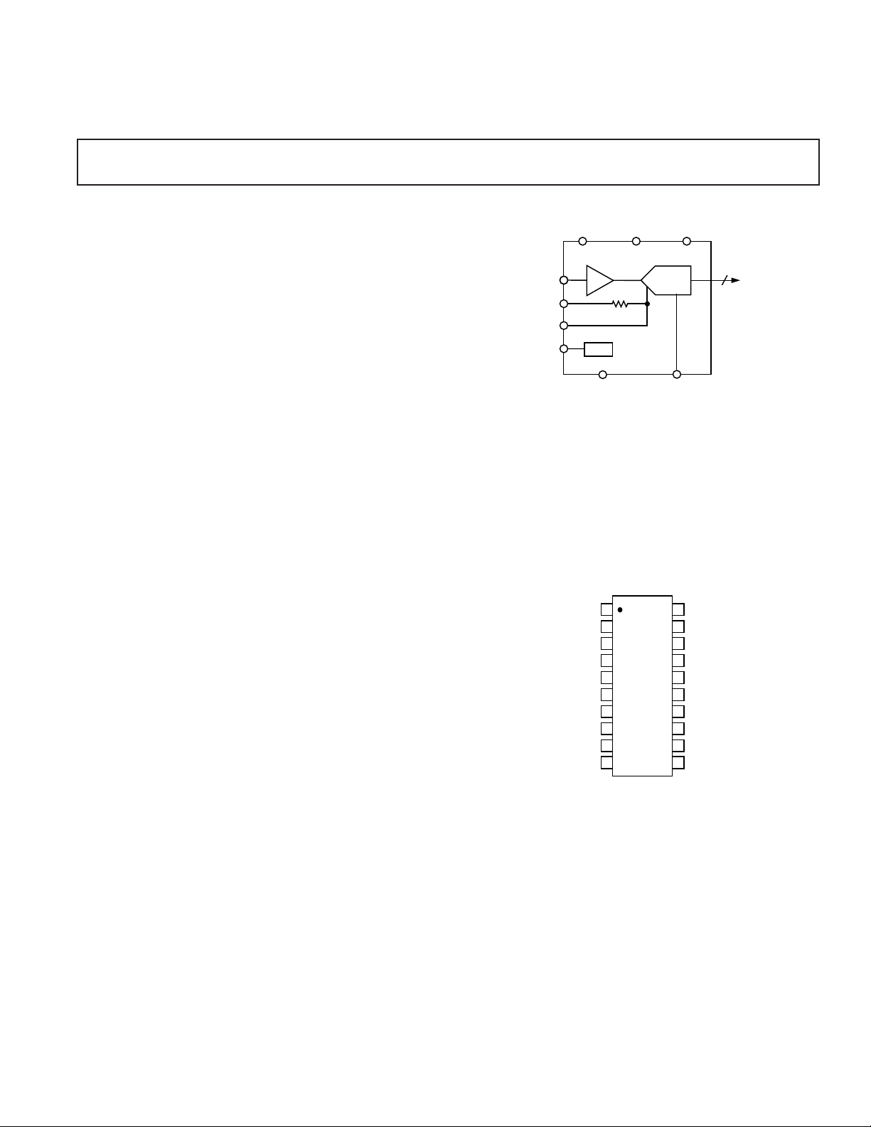
FUNCTIONAL BLOCK DIAGRAM
V
AIN
BIAS OUT
VREF IN
VREF OUT
Customers desiring multichannel digitization may consider the
AD9059, a dual 8-bit, 60 MSPS monolithic based on the
AD9057 ADC core. The AD9059 is available in a 28-lead surface mount plastic package (28 SSOP) and is specified over the
industrial temperature range.
PIN CONFIGURATION
PWRDN
VREF OUT
VREF IN
BIAS OUT
ENCODE
D
+2.5V
GND
V
AIN
V
GND
AD9057
1kΩ
GND
1
2
3
4
5
D
6
7
8
D
9
10
(Not to Scale)
PWRDN V
ADCT/H
ENCODE
AD9057
TOP VIEW
20
19
18
17
16
15
14
13
12
11
DD
D0 (LSB)
D1
D2
D3
GND
V
DD
D4
D5
D6
D7 (MSB)
8
D7–D0
REV. B
Information furnished by Analog Devices is believed to be accurate and
reliable. However, no responsibility is assumed by Analog Devices for its
use, nor for any infringements of patents or other rights of third parties
which may result from its use. No license is granted by implication or
otherwise under any patent or patent rights of Analog Devices.
One Technology Way, P.O. Box 9106, Norwood, MA 02062-9106, U.S.A.
Tel: 617/329-4700 World Wide Web Site: http://www.analog.com
Fax: 617/326-8703 © Analog Devices, Inc., 1997

AD9057–SPECIFICA TIONS
(VD = +5 V, VDD = +3 V; external reference)
Parameter Temp Level Min Typ Max Min Typ Max Min Typ Max Units
Test AD9057BRS-40 AD9057BRS-60 AD9057BRS-80
RESOLUTION 8 8 8 Bits
DC ACCURACY
Differential Nonlinearity +25°C I 0.75 1.9 0.75 1.9 0.75 1.9 LSB
Full VI 2.0 2.0 2.0 LSB
Integral Nonlinearity +25°C I 0.75 1.9 0.75 1.9 0.75 1.9 LSB
Full VI 2.0 2.0 2.0 LSB
No Missing Codes Full VI GUARANTEED GUARANTEED GUARANTEED
Gain Error
Gain Tempco
1
1
+25°C I –6 –2.5 +6 –6 –2.5 +6 –6 –2.5 +6 % FS
Full VI –8 +8 –8 +8 –8 +8 % FS
Full V ±70 ±70 ±70 ppm/°C
ANALOG INPUT
Input Voltage Range
(Centered at +2.5 V) +25°C V 1.0 1.0 1.0 V p-p
Input Offset Voltage +25°C I –15 ±0 +15 –15 ±0 +15 –15 ±0 +15 mV
Full VI –25 +25 –25 +25 –25 +25 mV
Input Resistance +25°C V 150 150 150 kΩ
Input Capacitance +25°CV222pF
Input Bias Current +25°CI 616 616 616µA
Full VI 25 25 25 µA
Analog Bandwidth +25°C V 120 120 120 MHz
BANDGAP REFERENCE
Output Voltage Full VI 2.4 2.5 2.6 2.4 2.5 2.6 2.4 2.5 2.6 V
Temperature Coefficient Full V ±10 ±10 ±10 ppm/°C
SWITCHING PERFORMANCE
Maximum Conversion Rate Full VI 40 60 80 MSPS
Minimum Conversion Rate Full IV 5 5 5 MSPS
Aperture Delay (t
Aperture Uncertainty (Jitter) +25°C V 5 5 5 ps, rms
Output Valid Time (t
) +25°C V 2.7 2.7 2.7 ns
A
2
)
V
Full IV 4.0 6.6 4.0 6.6 4.0 6.6 ns
Output Propagation Delay (tPD)2Full IV 11.5 18.0 9.5 14.2 8.0 11.3 ns
DYNAMIC PERFORMANCE
3
Transient Response +25°CV999ns
Overvoltage Recovery Time +25°CV999ns
Signal-to-Noise Ratio (SINAD)
(With Harmonics)
= 10.3 MHz +25°C I 42 45.5 42 45 41.5 45 dB
f
IN
= 76 MHz +25°C V 44.0 43.5 43.5 dB
f
IN
Effective Number of Bits
= 10.3 MHz +25°C I 6.7 7.2 6.7 7.2 6.6 7.2 Bits
f
IN
= 76 MHz +25°C V 7.0 6.9 6.9 Bits
f
IN
Signal-to-Noise Ratio (SNR)
(Without Harmonics)
= 10.3 MHz +25°C I 43 46.5 43 46 42.5 46 dB
f
IN
= 76 MHz +25°C V 45.5 45 45 dB
f
IN
2nd Harmonic Distortion
= 10.3 MHz +25°C I –50 –62 –50 –62 –50 –62 dBc
f
IN
= 76 MHz +25°C V –54 –54 –54 dBc
f
IN
3rd Harmonic Distortion
= 10.3 MHz +25°C I –46 –60 –46 –60 –46 –60 dBc
f
IN
= 76 MHz +25°C V –54 –54 –54 dBc
f
IN
Two Tone Intermodulation
Distortion (IMD) +25°C V –52 –52 –52 dBc
Differential Phase +25°C V 0.8 0.8 0.8 Degrees
Differential Gain +25°C V 1.0 1.0 1.0 %
DIGITAL INPUTS
Logic “1” Voltage Full VI 2.0 2.0 2.0 V
Logic “0” Voltage Full VI 0.8 0.8 0.8 V
Logic “1” Current Full VI ±1 ±1 ±1 µA
Logic “0” Current Full VI ±1 ±1 ±1 µA
Input Capacitance +25°C V 4.5 4.5 4.5 pF
Encode Pulse Width High (t
) +25°C IV 9.0 166 6.7 166 5.5 166 ns
EH
Encode Pulse Width Low (tEL) +25°C IV 9.0 166 6.7 166 5.5 166 ns
–2–
REV. B

AD9057
Parameter Temp Level Min Typ Max Min Typ Max Min Typ Max Units
Test AD9057BRS-40 AD9057BRS-60 AD9057BRS-80
DIGITAL OUTPUTS
Logic “1” Voltage (V
= +3 V) Full VI 2.95 V
DD
Logic “1” Voltage (VDD = +5 V) Full IV 4.95 V
Logic “0” Voltage Full VI 0.05 V Output Coding
Offset Binary Code
POWER SUPPLY
V
Supply Current (VD = +5 V) Full VI 36 48 38 48 40 51 mA
D
VDD Supply Current (VDD = +3 V)4Full VI 4.0 6.5 5.5 6.5 7.4 8.8 mA
Power Dissipation
5, 6
Full VI 192 260 205 260 220 281 mW
Power-Down Dissipation Full VI 6 10 6 10 6 10 mW
Power Supply Rejection Ratio
(PSRR) +25°C I 15 15 15 mV/V
NOTES
1
Gain error and gain temperature coefficient are based on the ADC only (with a fixed +2.5 V external reference).
2
tV and tPD are measured from the 1.5 V level of the ENCODE to the 10%/90% levels of the digital output swing. The digital output load during test is not to exceed
an ac load of 10 pF or a dc current of ±40 µA.
3
SNR/harmonics based on an analog input voltage of –0.5 dBFS referenced to a 1.0 V full-scale input range.
4
Digital supply current based on VDD = +3 V output drive with <10 pF loading under dynamic test conditions.
5
Power dissipation is based on specified encode and 10.3 MHz analog input dynamic test conditions (V
6
Typical thermal impedance for the RS style (SSOP) 20-pin package: θJC = 46°C/W, θCA = 80°C/W, θJA = 126°C/W.
= +5 V ± 5%, VDD = +3 V ± 5%).
D
Specifications subject to change without notice.
EXPLANATION OF TEST LEVELS
Test Level Description
I 100% Production Tested
II 100% Production Tested at +25°C and Sample
Tested at Specified Temperatures
III Sample Tested Only
IV Parameter is Guaranteed by Design and Char-
acterization Testing
V Parameter is a Typical Value Only
VI 100% Production Tested at +25°C; Guaran-
teed by Design and Characterization Testing
for Industrial Temperature Range
AIN
ENCODE
DIGITAL
OUTPUTS
N
N + 1
t
A
t
EH
N – 3 N – 2 N – 1 N N + 1 N + 2
N + 2
t
EL
N + 3
N + 4
t
V
t
PD
N + 5
REV. B
t
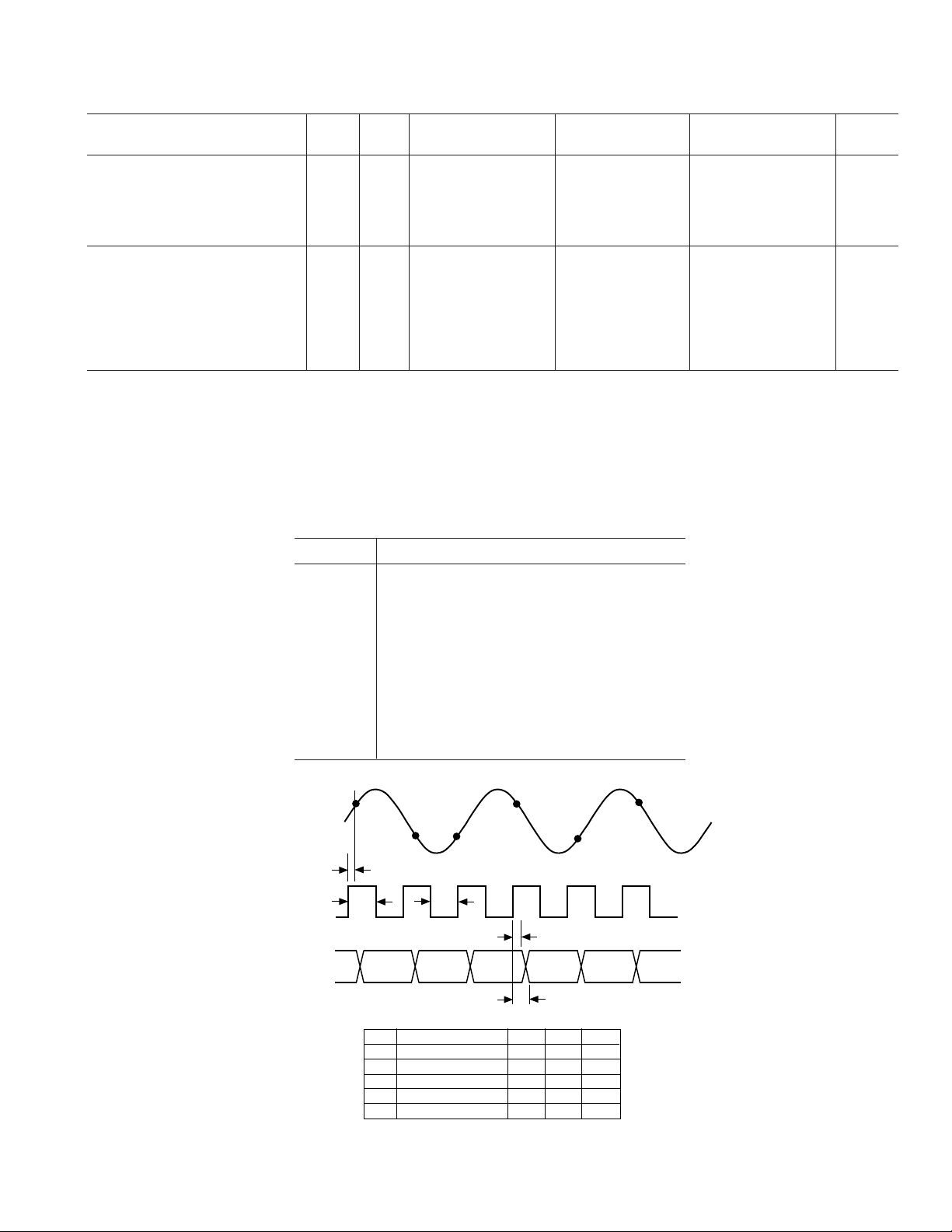
APERTURE DELAY
A
t
PULSE WIDTH HIGH
EH
t
PULSE WIDTH LOW
EL
t
V
OUTPUT VALID TIME
t
PD
OUTPUT PROP DELAY
Figure 1. Timing Diagram
–3–
MIN TYP MAX
2.7 ns
166 ns
166 ns
6.6 ns
4.0 ns
9.5 ns

AD9057
WARNING!
ESD SENSITIVE DEVICE
ABSOLUTE MAXIMUM RATINGS
VD, VDD . . . . . . . . . . . . . . . . . . . . . . . . . . . . . . . . . . . . . +7 V
Analog Inputs . . . . . . . . . . . . . . . . . . . . –0.5 V to V
Digital Inputs . . . . . . . . . . . . . . . . . . . . –0.5 V to V
V
Input . . . . . . . . . . . . . . . . . . . . . . . –0.5 V to VD + 0.5 V
REF
+ 0.5 V
D
+ 0.5 V
DD
Digital Output Current . . . . . . . . . . . . . . . . . . . . . . . . 20 mA
Operating Temperature . . . . . . . . . . . . . . . –55°C to +125°C
Storage Temperature . . . . . . . . . . . . . . . . . –65°C to +150°C
Maximum Junction Temperature . . . . . . . . . . . . . . . . +175°C
Maximum Case Temperature . . . . . . . . . . . . . . . . . . +150°C
ORDERING GUIDE
Temperature
Model Range Package Option*
AD9057BRS–40, –60, –80 –40° C to +85°C RS-20
AD9057/PCB +25°C Evaluation Board
*RS = Shrink Small Outline (SSOP).
Table I. Digital Coding (VREF = +2.5 V)
Analog Input Voltage Level Digital Output
3.0 V Positive Full Scale 1111 1111
2.502 V Midscale +1/2 LSB 1000 0000
2.498 V Midscale –1/2 LSB 0111 1111
2.0 Negative Full Scale 0000 0000
PIN DESCRIPTIONS
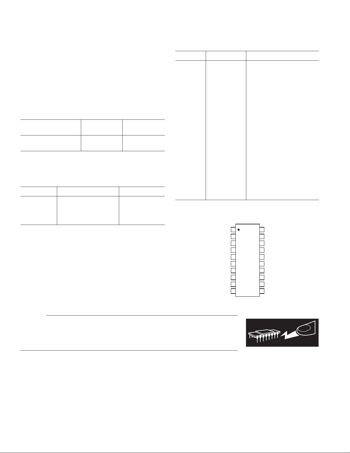
Pin No. Name Function
1 PWRDN Power-Down Function Select;
Logic HIGH for Power-Down
Mode (Digital Outputs Go to
High Impedance State).
2 VREF OUT Internal Reference Output
(+2.5 V typ); Bypass with
0.1 µF to Ground.
3 VREF IN Reference Input for ADC (+2.5
V typ, ±10%).
4, 9, 16 GND Ground (Analog/Digital).
5, 8 V
D
Analog +5 V Power Supply.
6 BIAS OUT Bias Pin for AC Coupling
(1 kΩ to REF IN).
7 AIN Analog Input for ADC.
10 ENCODE Encode Clock for ADC (ADC
Samples on Rising Edge of
ENCODE).
11–14, 17–20 D7–D4, D3–D0 Digital Outputs of ADC.
15 V
DD
Digital Output Power Supply.
Nominally +3 V to +5
V.
PIN CONFIGURATION
PWRDN
VREF OUT
VREF IN
GND
BIAS OUT
AIN
GND
ENCODE
V
D
V
D
1
2
3
4
AD9057
5
TOP VIEW
(Not to Scale)
6
7
8
9
10
20
19
18
17
16
15
14
13
12
11
D0 (LSB)
D1
D2
D3
GND
V
DD
D4
D5
D6
D7 (MSB)
CAUTION
ESD (electrostatic discharge) sensitive device. Electrostatic charges as high as 4000 V readily
accumulate on the human body and test equipment and can discharge without detection.
Although the AD9057 features proprietary ESD protection circuitry, permanent damage may
occur on devices subjected to high energy electrostatic discharges. Therefore, proper ESD
precautions are recommended to avoid performance degradation or loss of functionality.
–4–
REV. B
 Loading...