ANALOG DEVICES AD8551, AD8552 Service Manual

Zero-Drift, Single-Supply, Rail-to-Rail
–
A
+
A
A
Input/Output Operational Amplifiers
FEATURES
Low offset voltage: 1 μV
Input offset drift: 0.005 μV/°C
Rail-to-rail input and output swing
5 V/2.7 V single-supply operation
High gain, CMRR, PSRR: 130 dB
Ultralow input bias current: 20 pA
Low supply current: 700 μA/op amp
Overload recovery time: 50 μs
No external capacitors required
APPLICATIONS
Temperature sensors
Pressure sensors
Precision current sensing
Strain gage amplifiers
Medical instrumentation
Thermocouple amplifiers
GENERAL DESCRIPTION
This family of amplifiers has ultralow offset, drift, and bias
current. The AD8551, AD8552, and AD8554 are single, dual,
and quad amplifiers featuring rail-to-rail input and output swings.
All are guaranteed to operate from 2.7 V to 5 V with a single supply.
The AD855x family provides the benefits previously found only
in expensive auto-zeroing or chopper-stabilized amplifiers.
Using Analog Devices, Inc. topology, these new zero-drift
amplifiers combine low cost with high accuracy. No external
capacitors are required.
AD8551/AD8552/AD8554
PIN CONFIGURATIONS
18
NC
IN
AD8551
IN
V–
45
NC = NO CONNECT
Figure 1. 8-Lead MSOP (RM Suffix)
1
NC
–IN A
2
AD8551
+IN
3
V–
4
NC = NO CONNECT
Figure 2. 8-Lead SOIC (R Suffix)
OUT A
–IN A
+IN A
18
AD8552
V–
45
Figure 3. 8-Lead TSSOP (RU Suffix)
1
OUT A
–IN A
2
AD8552
+IN A
3
V–
4
Figure 4. 8-Lead SOIC (R Suffix)
OUT A
–IN A
+IN A
+IN B
–IN B
OUT B
114
V+
AD8554
78
Figure 5. 14-Lead TSSOP (RU Suffix)
8
7
6
5
8
7
6
5
NC
V+
OUT A
NC
NC
V+
OUT A
NC
V+
OUT B
–IN B
+IN B
V+
OUT B
–IN B
+IN B
OUT D
–IN D
+IN D
V–
+IN C
–IN C
OUT C
1101-001
1101-002
01101-003
01101-004
1101-005
With an offset voltage of only 1 μV and drift of 0.005 μV/°C, the
AD855x are perfectly suited for applications in which error
sources cannot be tolerated. Temperature, position and pressure
sensors, medical equipment, and strain gage amplifiers benefit
greatly from nearly zero drift over their operating temperature
range. The rail-to-rail input and output swings provided by the
AD855x family make both high-side and low-side sensing easy.
The AD855x family is specified for the extended industrial/auto
1
OUT A
–IN A
+IN A
+IN B
–IN B
OUT B
2
3
4
V+
AD8554
5
6
7
14
13
12
11
10
9
8
OUT D
–IN D
+IN D
V–
+IN C
–IN C
OUT C
Figure 6. 14-Lead SOIC (R Suffix)
01101-006
motive temperature range (−40°C to +125°C). The AD8551
single amplifier is available in 8-lead MSOP and 8-lead narrow
SOIC packages. The AD8552 dual amplifier is available in 8-lead
narrow SOIC and 8-lead TSSOP surface-mount packages. The
AD8554 quad is available in 14-lead narrow SOIC and 14-lead
TSSOP packages.
Rev. D
Information furnished by Analog Devices is believed to be accurate and reliable. However, no
responsibility is assumed by Analog Devices for its use, nor for any infringements of patents or other
rights of third parties that may result from its use. Specifications subject to change without notice. No
license is granted by implication or otherwise under any patent or patent rights of Analog Devices.
Trademarks and registered trademarks are the property of their respective owners.
One Technology Way, P.O. Box 9106, Norwood, MA 02062-9106, U.S.A.
Tel: 781.329.4700 www.analog.com
Fax: 781.461.3113 ©1999–2008 Analog Devices, Inc. All rights reserved.

AD8551/AD8552/AD8554
TABLE OF CONTENTS
Features .............................................................................................. 1
1/f Noise Characteristics ........................................................... 17
Applications ....................................................................................... 1
General Description ......................................................................... 1
Pin Configurations ........................................................................... 1
Revision History ............................................................................... 2
Specifications ..................................................................................... 3
Electrical Characteristics ............................................................. 3
Absolute Maximum Ratings ............................................................ 5
Thermal Characteristics .............................................................. 5
ESD Caution .................................................................................. 5
Typical Performance Characteristics ............................................. 6
Functional Description .................................................................. 14
Amplifier Architecture .............................................................. 14
Basic Auto-Zero Amplifier Theory .......................................... 14
High Gain, CMRR, PSRR .......................................................... 16
Maximizing Performance Through Proper Layout ............... 16
Intermodulation Distortion ...................................................... 17
Broadband and External Resistor Noise Considerations ...... 18
Output Overdrive Recovery ...................................................... 18
Input Overvoltage Protection ................................................... 18
Output Phase Reversal ............................................................... 19
Capacitive Load Drive ............................................................... 19
Power-Up Behavior .................................................................... 19
Applications ..................................................................................... 20
A 5 V Precision Strain Gage Circuit ........................................ 20
3 V Instrumentation Amplifier ................................................ 20
A High Accuracy Thermocouple Amplifier ........................... 21
Precision Current Meter ............................................................ 21
Precision Voltage Comparator .................................................. 21
Outline Dimensions ....................................................................... 22
Ordering Guide .......................................................................... 23
REVISION HISTORY
9/08—Rev. C to Rev. D
Changes to Ordering Guide .......................................................... 23
3/07—Rev. B to Rev. C
Changes to Specifications Section .................................................. 3
2/07—Rev. A to Rev. B
Updated Format .................................................................. Universal
Changes to Figure 54 ...................................................................... 16
Deleted Spice Model Section ......................................................... 19
Deleted Figure 63, Renumbered Sequentially ............................ 19
Changes to Ordering Guide .......................................................... 24
11/02—Rev. 0 to Rev. A
Edits to Figure 60 ............................................................................ 16
Updated Outline Dimensions ....................................................... 20
Rev. D | Page 2 of 24

AD8551/AD8552/AD8554
SPECIFICATIONS
ELECTRICAL CHARACTERISTICS
VS = 5 V, VCM = 2.5 V, VO = 2.5 V, TA = 25°C, unless otherwise noted.
Table 1.
Parameter Symbol Conditions Min Typ Max Unit
INPUT CHARACTERISTICS
Offset Voltage VOS 1 5 μV
−40°C ≤ TA ≤ +125°C 10 μV
Input Bias Current IB 10 50 pA
AD8551/AD8554 −40°C ≤ TA ≤ +125°C 1.0 1.5 nA
AD8552 −40°C ≤ TA ≤ +85°C 160 300 pA
AD8552 −40°C ≤ TA ≤ +125°C 2.5 4 nA
Input Offset Current IOS 20 70 pA
AD8551/AD8554 −40°C ≤ TA ≤ +125°C 150 200 pA
AD8552 −40°C ≤ TA ≤ +85°C 30 150 pA
AD8552 −40°C ≤ TA ≤ +125°C 150 400 pA
Input Voltage Range 0 5 V
Common-Mode Rejection Ratio CMRR VCM = 0 V to +5 V 120 140 dB
−40°C ≤ TA ≤ +125°C 115 130 dB
Large Signal Voltage Gain1 AVO RL = 10 kΩ, VO = 0.3 V to 4.7 V 125 145 dB
−40°C ≤ TA ≤ +125°C 120 135 dB
Offset Voltage Drift ΔVOS/ΔT −40°C ≤ TA ≤ +125°C 0.005 0.04 μV/°C
OUTPUT CHARACTERISTICS
Output Voltage High VOH RL = 100 kΩ to GND 4.99 4.998 V
R
R
R
Output Voltage Low V
R
OL
R
R
R
Output Short-Circuit Limit Current ISC ±25 ±50 mA
−40°C to +125°C ±40 mA
Output Current IO ±30 mA
−40°C to +125°C ±15 mA
POWER SUPPLY
Power Supply Rejection Ratio PSRR VS = 2.7 V to 5.5 V 120 130 dB
−40°C ≤ TA ≤ +125°C 115 130 dB
Supply Current/Amplifier ISY VO = 0 V 850 975 μA
−40°C ≤ TA ≤ +125°C 1000 1075 μA
DYNAMIC PERFORMANCE
Slew Rate SR RL = 10 kΩ 0.4 V/μs
Overload Recovery Time 0.05 0.3 ms
Gain Bandwidth Product GBP 1.5 MHz
NOISE PERFORMANCE
Voltage Noise en p-p 0 Hz to 10 Hz 1.0 μV p-p
e
p-p 0 Hz to 1 Hz 0.32 μV p-p
n
Voltage Noise Density en f = 1 kHz 42 nV/√Hz
Current Noise Density in f = 10 Hz 2 fA/√Hz
1
Gain testing is dependent upon test bandwidth.
= 100 kΩ to GND @ −40°C to +125°C 4.99 4.997 V
L
= 10 kΩ to GND 4.95 4.98 V
L
= 10 kΩ to GND @ −40°C to +125°C 4.95 4.975 V
L
= 100 kΩ to V+ 1 10 mV
L
= 100 kΩ to V+ @ −40°C to +125°C 2 10 mV
L
= 10 kΩ to V+ 10 30 mV
L
= 10 kΩ to V+ @ −40°C to +125°C 15 30 mV
L
Rev. D | Page 3 of 24

AD8551/AD8552/AD8554
VS = 2.7 V, VCM = 1.35 V, VO = 1.35 V, TA = 25°C, unless otherwise noted.
Table 2.
Parameter Symbol Conditions Min Typ Max Unit
INPUT CHARACTERISTICS
Offset Voltage VOS 1 5 μV
−40°C ≤ TA ≤ +125°C 10 μV
Input Bias Current IB 10 50 pA
AD8551/AD8554 −40°C ≤ TA ≤ +125°C 1.0 1.5 nA
AD8552 −40°C ≤ TA ≤ +85°C 160 300 pA
AD8552 −40°C ≤ TA ≤ +125°C 2.5 4 nA
Input Offset Current I
AD8551/AD8554 −40°C ≤ TA ≤ +125°C 150 200 pA
AD8552 −40°C ≤ TA ≤ +85°C 30 150 pA
AD8552 −40°C ≤ TA ≤ +125°C 150 400 pA
Input Voltage Range 0 2.7 V
Common-Mode Rejection Ratio CMRR VCM = 0 V to 2.7 V 115 130 dB
−40°C ≤ TA ≤ +125°C 110 130 dB
Large Signal Voltage Gain1 AVO RL = 10 kΩ, VO = 0.3 V to 2.4 V 110 140 dB
−40°C ≤ TA ≤ +125°C 105 130 dB
Offset Voltage Drift ΔVOS/ΔT −40°C ≤ TA ≤ +125°C 0.005 0.04 μV/°C
OUTPUT CHARACTERISTICS
Output Voltage High VOH RL = 100 kΩ to GND 2.685 2.697 V
R
R
R
Output Voltage Low VOL RL = 100 kΩ to V+ 1 10 mV
R
R
R
Short-Circuit Limit ISC ±10 ±15 mA
−40°C to +125°C ±10 mA
Output Current IO ±10 mA
−40°C to +125°C ±5 mA
POWER SUPPLY
Power Supply Rejection Ratio PSRR VS = 2.7 V to 5.5 V 120 130 dB
−40°C ≤ TA ≤ +125°C 115 130 dB
Supply Current/Amplifier ISY VO = 0 V 750 900 μA
−40°C ≤ TA ≤ +125°C 950 1000 μA
DYNAMIC PERFORMANCE
Slew Rate SR RL = 10 kΩ 0.5 V/μs
Overload Recovery Time 0.05 ms
Gain Bandwidth Product GBP 1 MHz
NOISE PERFORMANCE
Voltage Noise en p-p 0 Hz to 10 Hz 1.6 μV p-p
Voltage Noise Density en f = 1 kHz 75 nV/√Hz
Current Noise Density in f = 10 Hz 2 fA/√Hz
1
Gain testing is dependent upon test bandwidth.
10 50 pA
OS
= 100 kΩ to GND @ −40°C to +125°C 2.685 2.696 V
L
= 10 kΩ to GND 2.67 2.68 V
L
= 10 kΩ to GND @ −40°C to +125°C 2.67 2.675 V
L
= 100 kΩ to V+ @ −40°C to +125°C 2 10 mV
L
= 10 kΩ to V+ 10 20 mV
L
= 10 kΩ to V+ @ −40°C to +125°C 15 20 mV
L
Rev. D | Page 4 of 24

AD8551/AD8552/AD8554
ABSOLUTE MAXIMUM RATINGS
Table 3.
Parameter Rating
Supply Voltage 6 V
Input Voltage GND to VS + 0.3 V
Differential Input Voltage1 ±5.0 V
ESD (Human Body Model) 2000 V
Output Short-Circuit Duration to GND Indefinite
Storage Temperature Range −65°C to +150°C
Operating Temperature Range −40°C to +125°C
Junction Temperature Range −65°C to +150°C
Lead Temperature Range (Soldering, 60 sec) 300°C
1
Differential input voltage is limited to ±5.0 V or the supply voltage,
whichever is less.
THERMAL CHARACTERISTICS
Table 4.
Package Type θJA θ
8-Lead MSOP (RM) 190 44 °C/W
8-Lead TSSOP (RU) 240 43 °C/W
8-Lead SOIC (R) 158 43 °C/W
14-Lead TSSOP (RU) 180 36 °C/W
14-Lead SOIC (R) 120 36 °C/W
Unit
JC
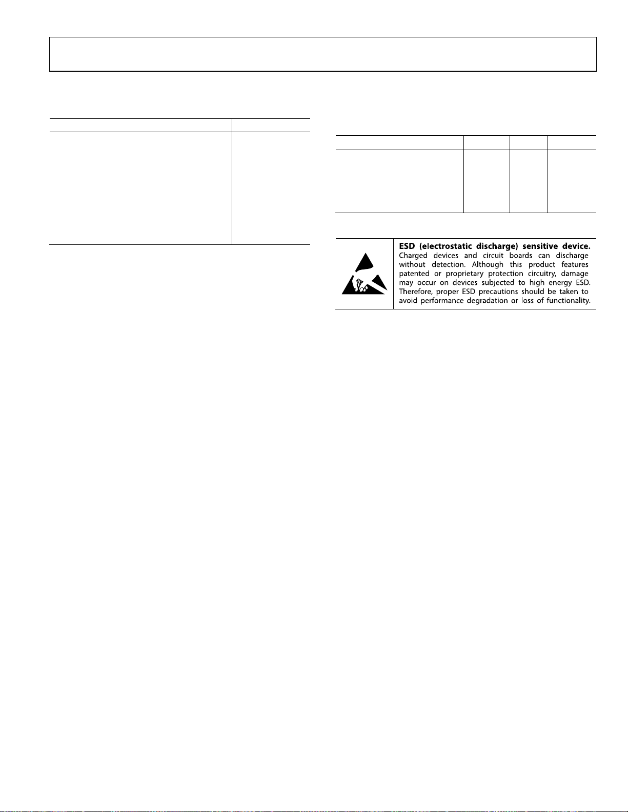
ESD CAUTION
Stresses above those listed under Absolute Maximum Ratings
may cause permanent damage to the device. This is a stress
rating only; functional operation of the device at these or any
other conditions above those indicated in the operational
section of this specification is not implied. Exposure to absolute
maximum rating conditions for extended periods may affect
device reliability.
Rev. D | Page 5 of 24

AD8551/AD8552/AD8554
TYPICAL PERFORMANCE CHARACTERISTICS
180
160
140
120
100
80
60
NUMBER OF AMPL IFIERS
40
20
0
–2.5
–1.5 –0. 5
OFFSET VOLTAGE (µV)
0.5
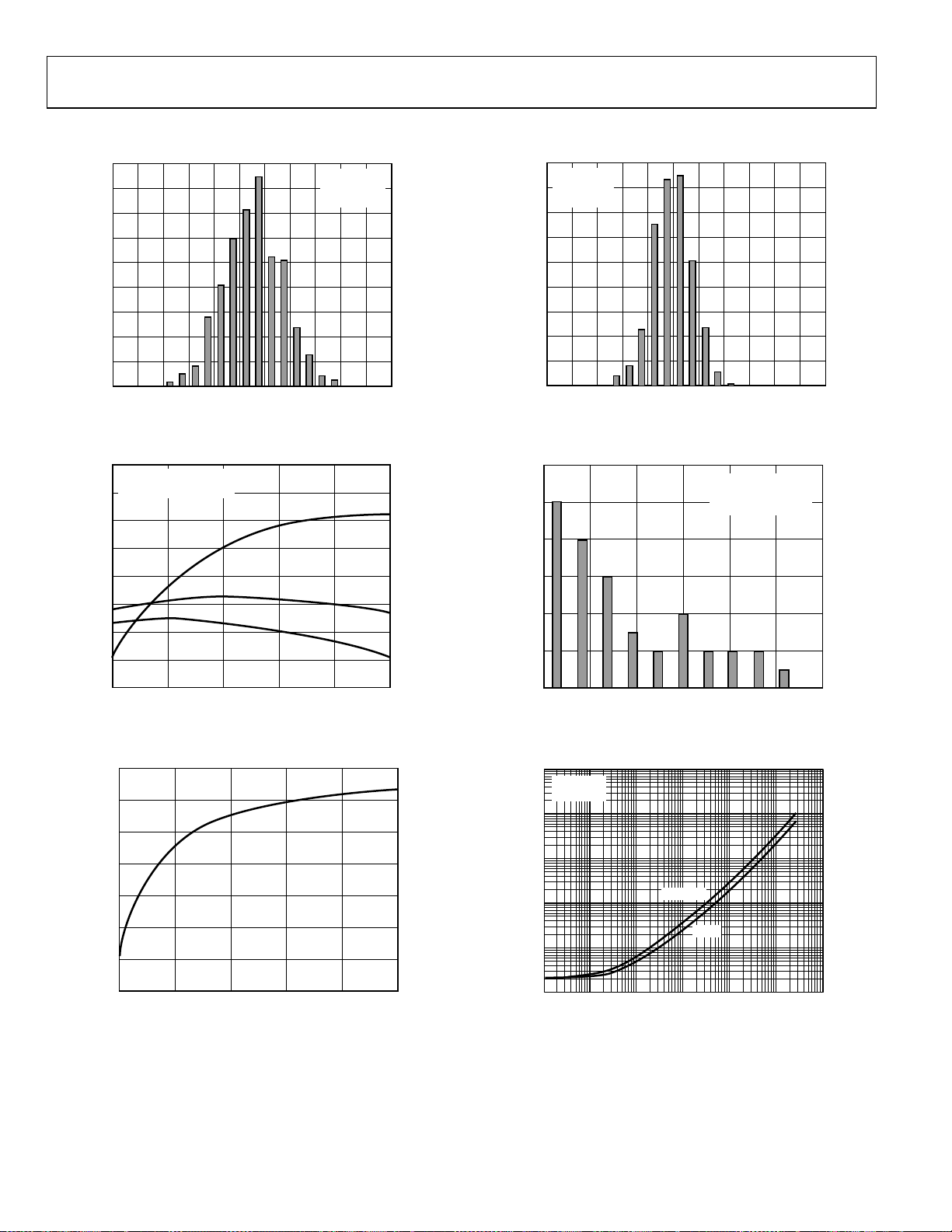
Figure 7. Input Offset Voltage Distribution at 2.7 V
VSY = 2.7V
V
T
1.5
CM
= 25°C
A
= 1.35V
2.5
01101-007
180
VSY = 5V
V
160
140
120
100
NUMBER OF AMPLIFIERS
= 2.5V
CM
T
= 25°C
A
80
60
40
20
0
–2.5 –1.5 –0.5 1.5
OFFSET VOLTAGE (µV)
0.5 2.5
Figure 10. Input Offset Voltage Distribution at 5 V
01101-010
50
VSY = 5V
T
= –40°C, +25° C, +85°C
A
40
30
20
10
0
INPUT BIAS CURRENT (pA)
–10
–20
–30
012 34
INPUT COMMON-MODE VOLTAGE (V)
+85°C
+25°C
–40°C
Figure 8. Input Bias Current vs. Common-Mode Voltage
1500
V
= 5V
SY
T
= 125°C
A
1000
500
0
–500
–1000
INPUT BIAS CURRENT (pA)
–1500
12
10
8
6
4
NUMBER OF AMPLI FIERS
2
5
01101-008
0
0123456
INPUT OFFSET DRIFT (nV/°C)
VSY = 5V
V
= 2.5V
CM
T
= –40°C TO +125°C
A
01101-011
Figure 11. Input Offset Voltage Drift Distribution at 5 V
10k
VSY = 5V
T
= 25°C
A
1k
100
10
OUTPUT VOLTAGE (mV)
1
SOURCE
SINK
–2000
01234
INPUT COMMON-MODE VOLTAGE (V)
Figure 9. Input Bias Current vs. Common-Mode Voltage
5
01101-009
Rev. D | Page 6 of 24
0.1
0.0001 0.001 0.01 0.1 1 10 100
LOAD CURRENT (mA)
Figure 12. Output Voltage to Supply Rail vs. Load Current at 5 V
01101-012

AD8551/AD8552/AD8554
10k
1k
VSY = 2.7V
T
= 25°C
A
800
700
600
TA = +25°C
100
10
OUTPUT VOLTAGE (mV)
1
0.1
0.0001 0.001 0.01 0.1 1 10 100
SOURCE
SINK
LOAD CURRENT (mA)
Figure 13. Output Voltage to Supply Rail vs. Load Current at 2.7 V
0
VCM = 2.5V
V
= 5V
SY
–250
–500
–750
INPUT BIAS CURRENT (pA)
–1000
–75 –50 125–25 100
0255075
TEMPERATURE ( °C)
Figure 14. Input Bias Current vs. Temperature
150
500
400
300
200
100
SUPPLY CURRENT PER AMPLIFI ER (µA)
0
061
01101-013
2345
SUPPLY VOLTAGE (V)
1101-016
Figure 16. Supply Current per Amplifier vs. Supply Voltage
60
VSY = 2.7V
50
40
30
20
10
0
–10
OPEN-LOOP GAIN (dB)
–20
–30
–40
10k 100k 1M 10M 100M
01101-014
C
R
= 0pF
L
=
L
∞
FREQUENCY (Hz)
0
45
90
135
180
225
270
PHASE SHIFT (Degrees)
01101-017
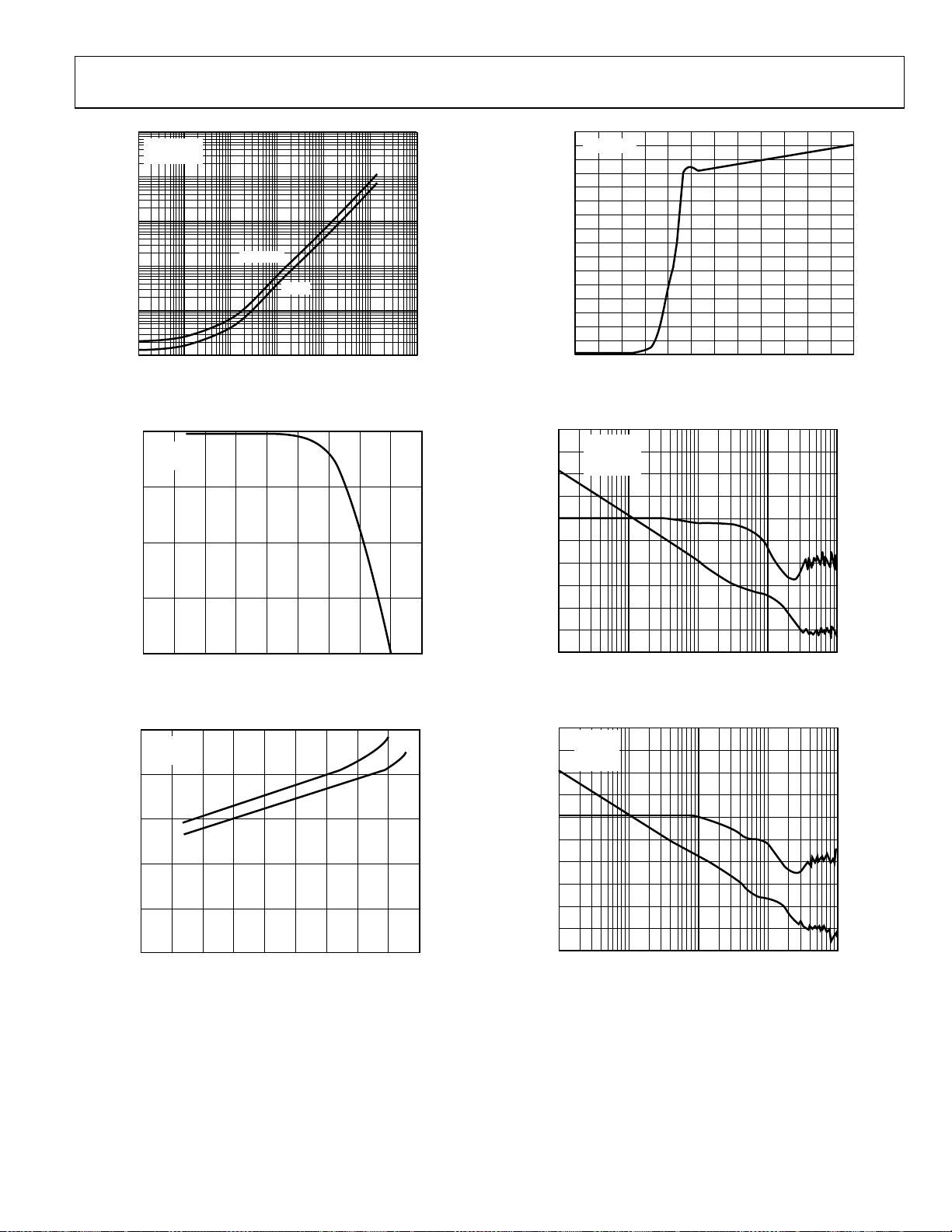
Figure 17. Open-Loop Gain and Phase Shift vs. Frequency at 2.7 V
1.0
VCM = 2.5V
V
= 5V
SY
0.8
0.6
0.4
SUPPLY CURRENT (mA)
0.2
0
–75 –50 125–25 100 150
0255075
TEMPERATURE ( °C)
5V
2.7V
Figure 15. Supply Current vs. Temperature
01101-015
Rev. D | Page 7 of 24
60
VSY = 5V
= 0pF
C
50
L
=
R
∞
L
40
30
20
10
0
–10
OPEN-LOOP GAIN (dB)
–20
–30
–40
10k 100k 1M 10M 100M
FREQUENCY (Hz)
Figure 18. Open-Loop Gain and Phase Shift vs. Frequency at 5 V
0
45
90
135
180
225
270
PHASE SHIFT (Degrees)
1101-018

AD8551/AD8552/AD8554
60
50
AV = –100
40
30
AV = –10
20
10
AV = +1
0
–10
CLOSED-LOOP GAIN (dB)
–20
–30
–40
1k
10k 100k 1M 10M100
FREQUENCY (Hz)
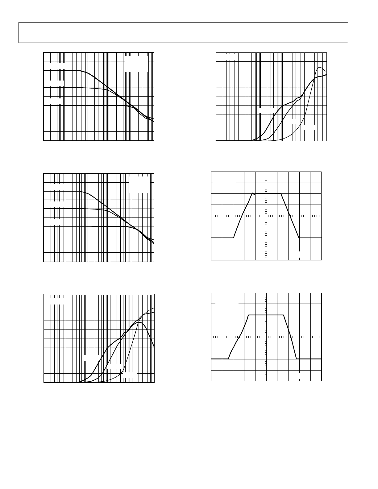
Figure 19. Closed-Loop Gain vs. Frequency at 2.7 V
VSY = 2.7V
= 0pF
C
L
= 2kΩ
R
L
01101-019
300
VSY = 5V
270
240
210
180
150
120
90
OUTPUT IMPEDANCE (Ω)
60
30
0
AV = 100
10k 100k 1M 10M100 1k
FREQUENCY (Hz)
Figure 22. Output Impedance vs. Frequency at 5 V
AV = 10
AV = 1
01101-022
60
50
AV = –100
40
30
AV = –10
20
10
AV = +1
0
–10
CLOSED-LOOP GAIN (dB)
–20
–30
–40
1k
10k 100k 1M 10M100
FREQUENCY (Hz)
Figure 20. Closed-Loop Gain vs. Frequency at 5 V
300
VSY = 2.7V
270
240
210
180
150
120
90
OUTPUT IMPEDANCE (Ω)
60
30
0
AV = 100
AV = 10
10k 100k 1M 10M100 1k
FREQUENCY (Hz)
Figure 21. Output Impedance vs. Frequency at 2.7 V
AV = 1
VSY = 5V
= 0pF
C
L
= 2kΩ
R
L
VSY = 2.7V
= 300pF
C
L
= 2kΩ
R
L
= 1
A
V
2µs
01101-020
500mV
01101-023
Figure 23. Large Signal Transient Response at 2.7 V
VSY = 5V
= 300pF
C
L
= 2kΩ
R
L
= 1
A
V
5µs
01101-021
1V
1101-024
Figure 24. Large Signal Transient Response at 5 V
Rev. D | Page 8 of 24
 Loading...