Analog Devices AD8522 Datasheet

+5 Volt, Serial Input,
PDIP-14
SO-14
a
FEATURES
Complete Dual 12-Bit DAC
No External Components
+5 V Single-Supply Operation 610%
4.095 V Full Scale (1 mV/LSB)
Buffered Voltage Outputs
Low Power: 5 mW/DAC
Space Saving 1.5 mm Height SO-14 Package
APPLICATIONS
Digitally Controlled Calibration
Servo Controls
Process Control Equipment
Computer Peripherals
Portable Instrumentation
Cellular Base Stations Voltage Adjustment
GENERAL DESCRIPTION
The AD8522 is a complete dual 12-bit, single-supply, voltage
output DAC in a 14-pin DIP, or SO-14 surface mount package.
Fabricated in a CBCMOS process, features include a serial digital interface, onboard reference, and buffered voltage output.
Ideal for +5 V-only systems, this monolithic device offers low
cost and ease of use, and requires no external components to
realize the full performance of the device.
The serial digital interface allows interfacing directly to numerous microcontroller ports, with a simple high speed, three-wire
data, clock, and load strobe format. The 16-bit serial word contains the 12-bit data word and DAC select address, which is decoded internally or can be decoded externally using
LDA, LDB
Dual 12-Bit DAC
AD8522
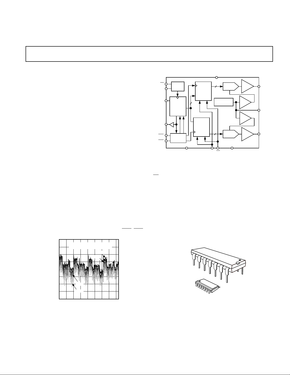
FUNCTIONAL BLOCK DIAGRAM
V
DD
CS
CLK
SDI
(DATA)
SDO
LDA
LDB
CLK
LATCH
SHIFT
REGISTER
CONTROL
LOGIC
DGND
DAC A
REGISTER
D
12
D
DAC B
REGISTER
12
12
MSB
DAC A
BANDGAP
REFERENCE
DAC B
AD8522
RS
inputs. A serial data output allows the user to easily daisy-chain
multiple devices in conjunction with a chip select input. A reset
RS input sets the outputs to zero scale or midscale, as determined by the input MSB.
The output 4.095 V full scale is laser trimmed to maintain accuracy over the operating temperature range of the device, and
gives the user an easy-to-use one-millivolt-per-bit resolution. A
2.5 V reference output is also available externally for other data
acquisition circuitry, and for ratiometric applications. The output buffers are capable of driving ± 5 mA.
The AD8522 is available in the 14-pin plastic DIP and low profile 1.5 mm SOIC-14 packages.
AGND
REF
BUF
REF
BUF
OP
AMP
A
OP
AMP
B
V
V
V
OUTA
REF
OUTB
0.6
0.4
0.2
–0.2
–0.4
–0.6
LINEARITY ERROR – LSB
–0.8
–1.0
VDD = +4.5V
= –55°C, +25°C, +85°C, +125°C
T
A
0
+85°C
+125°C
DIGITAL INPUT CODE – Decimal
+25°C
–55°C
40960 30721024 2048
Figure 1. Linearity Error vs. Digital Code & Temperature
REV. A
Information furnished by Analog Devices is believed to be accurate and
reliable. However, no responsibility is assumed by Analog Devices for its
use, nor for any infringements of patents or other rights of third parties
which may result from its use. No license is granted by implication or
otherwise under any patent or patent rights of Analog Devices.
PACKAGE TYPES AVAILABLE
One Technology Way, P.O. Box 9106, Norwood. MA 02062-9106, U.S.A.
Tel: 617/329-4700 Fax: 617/326-8703

AD8522–SPECIFICA TIONS
(@ VDD = +5.0 V 6 10%, RL = No Load, –408C ≤ TA ≤ +858C, both DACs tested, unless
ELECTRICAL CHARACTERISTICS
Parameter Symbol Condition Min Typ Max Units
STATIC PERFORMANCE
Resolution
Relative Accuracy INL -1.5 ±0.5 +1.5 LSB
Differential Nonlinearity DNL Monotonic -1 ±0.5 +1 LSB
Zero-Scale Error V
Full-Scale Voltage
Full-Scale Tempco
MATCHING PERFORMANCE
Linearity Matching Error ∆VFSA/B ±1 LSB
ANALOG OUTPUT
Output Current I
Load Regulation at Half-Scale LD
Capacitive Load
REFERENCE OUTPUT
Output Voltage V
Output Source Current
Line Rejection LN
Load Regulation LD
LOGIC INPUTS & OUTPUTS
Logic Input Low Voltage V
Logic Input High Voltage V
Input Leakage Current I
Input Capacitance
Logic Output Voltage Low V
Logic Output Voltage High V
TIMING SPECIFICATIONS
Clock Width High t
Clock Width Low t
Load Pulse Width t
Data Setup t
Data Hold t
Clear Pulse Width t
Load Setup t
Load Hold t
Select t
Deselect t
Clock to SDO Propagation Delay t
AC CHARACTERISTICS
Voltage Output Settling Time6t
Crosstalk C
DAC Glitch Q Half-Scale Transition 13 nV s
Digital Feedthrough D
SUPPLY CHARACTERISTICS
Positive Supply Current I
Power Dissipation
Power Supply Sensitivity PSS ∆VDD = ±5% 0.002 0.004 %/%
NOTES
1
1 LSB = 1 mV for 0 V to +4.095 V output range.
2
Includes internal voltage reference error.
3
These parameters are guaranteed by design and not subject to production testing.
4
Very little sink current is available at the V
5
All input control signals are specified with tr = tf = 5 ns (10% to 90% of +5 V) and timed from a voltage level of 1.6 V.
6
The settling time specification does not apply for negative going transitions within the last 6 LSBs of ground. Some devices exhibit double the typical settling time in this 6 LSB region.
7
Power Dissipation is calculated IDD × 5 V.
Specifications subject to change without notice.
1
2
2, 3
3
4
3
3, 5
3, 5
7
N 12 Bits
ZSE
V
FS
TCV
OUT
C
L
REF
I
REF
IL
IH
IL
C
IL
OL
OH
CH
CL
LDW
DS
DH
CLRW
LD1
LD2
CSS
CSH
PD
S
T
FT
DD
P
DISS
pin. Use external buffer if setting up a virtual ground.
REF
otherwise noted)
FS
REG
REJ
REG
Data = 000
Data = FFF
H
H
4.079 4.095 4.111 Volts
+0.5 +3 mV
±15 ppm/°C
Data = 800H, ∆V
RL = 402 Ω to ∞, Data = 800
≤ 3 LSB ±5mA
OUT
H
1 3 LSB
No Oscillation 500 pF
2.484 2.500 2.516 V
∆V
< 18 mV 5 mA
REF
0.025 0.08 %/V
I
= 0 to 5 mA, Data = 800
REF
H
0.025 0.1 %/mA
0.8 V
2.4 V
10 µA
10 pF
IOL = 1.6 mA 0.4 V
IOH = 400 µA 3.5 V
35 ns
35 ns
25 ns
10 ns
20 ns
20 ns
10 ns
10 ns
30 ns
30 ns
20 45 80 ns
To ±1 LSB of Final Value 16 µs
Signal Measured at DAC Output,
While Changing Opposite
LDA/B 38 dB
Signal Measured at DAC Output,
While Changing Data Without LDA/B 2 nV s
VDD = 5.5 V, VIH = 2.4 V or VIL = 0.8 V 3 5 mA
= 5 V, VIL = 0 V 1 2 mA
V
DD
VDD = 5 V, VIH = 2.4 V or VIL = 0.8 V 15 25 mW
= 5 V, VIL = 0 V 5 10 mW
V
DD
–2–
REV. A

AD8522
NC
CL
tDSt
DB11 DB10
DH
t
LD2
DB4 DB3 DB2 DB1 DB0
t
LDW
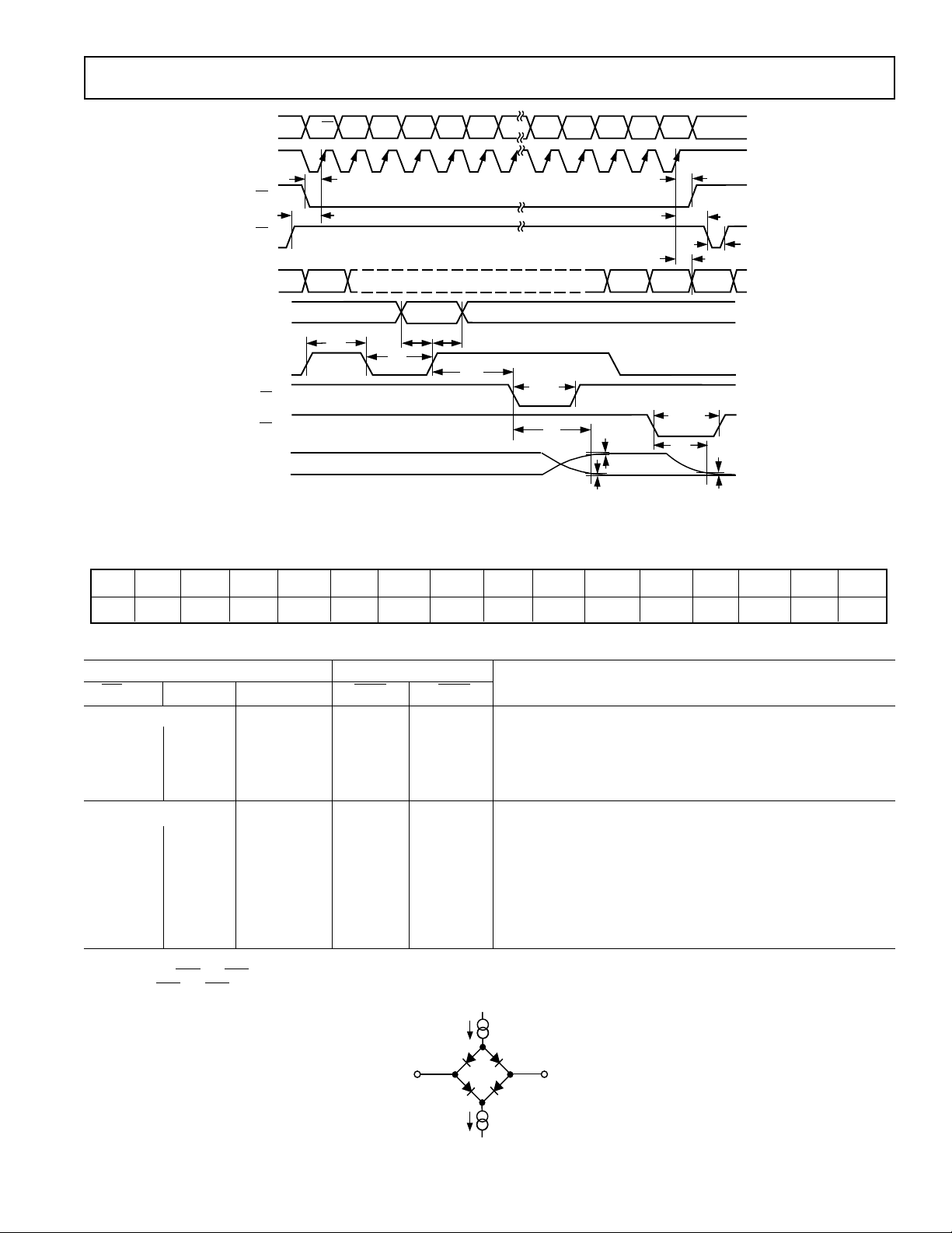
Figure 2. Timing Diagram
t
CSH
t
LD2
t
t
PD
t
t
S
±1 LSB
ERROR BAND
CLRW
t
S
LDW
SDI
CLK
SDO
CLK
V
CS
LD
SDI
LD
RS
OUT
Sf/Hd
t
LD1
t
CH
FS
ZS
t
AB
CSS
t
SERIAL INPUT REGISTER DATA FORMAT
Last First
D0 D1 D2 D3 D4 D5 D6 D7 D8 D9 D10 D11 D12 D13 D14 D15
DB0 DB1 DB2 DB3 DB4 DB5 DB6 DB7 DB8 DB9 DB10 DB11 NC A B Sf/Hd
Table I. Truth Table
Data Word Ext Pins
Sf/Hd BALDA LDB DAC Register
Hardware Load:
LXX↓↓Loads DACA + DACB with Data from SR
LXX↓H Loads DACA with Data from SR
L XXH↓Loads DACB with Data from SR
L X X H H No Load
Software Decode Load:
H L L X X No Load
HHL↓↓Loads DACB with Data from SR, See Note 1 Below
H H L H H No Load
HLH↓↓Loads DACA with Data from SR, See Note 1 Below
H L H H H No Load
HHH↓↓Loads DACA + DACB with Data from SR, See 1 Note Below
H H H H H No Load
NOTES
1
In software mode LDA and LDB perform the same function. They can be tied together or the unused pin should be tied high.
2
External Pins LDA and LDB should always be high when shifting Data into the shift register.
3
↓ symbol denotes negative transition.
1.6mA
REV. A
SDO
200µA
1.6 VOLT
Figure 3. AC Timing SDO Pin Load Circuit
–3–
 Loading...