

Page 1
Precision Thermocouple Amplifiers
FEATURES
Low cost and easy to use
Pretrimmed for J or K type thermocouples
Internal cold junction compensation
High impedance differential input
Standalone 5 mV/°C thermometer
Reference pin allows offset adjustment
Thermocouple break detection
Laser wafer trimmed to 1°C initial accuracy and
0.025°C/°C ambient temperature rejection
Low power: <1 mW at V
Wide power supply range
Single supply: 2.7 V to 36 V
Dual supply: ±2.7 V to ±18 V
Small, 8-lead MSOP
APPLICATIONS
J or K type thermocouple temperature measurement
Setpoint controller
Celsius thermometer
Universal cold junction compensator
White goods (oven, stove top) temperature measurements
Exhaust gas temperature sensing
Catalytic converter temperature sensing
= 5 V
S
with Cold Junction Compensation
AD8494/AD8495/AD8496/AD8497
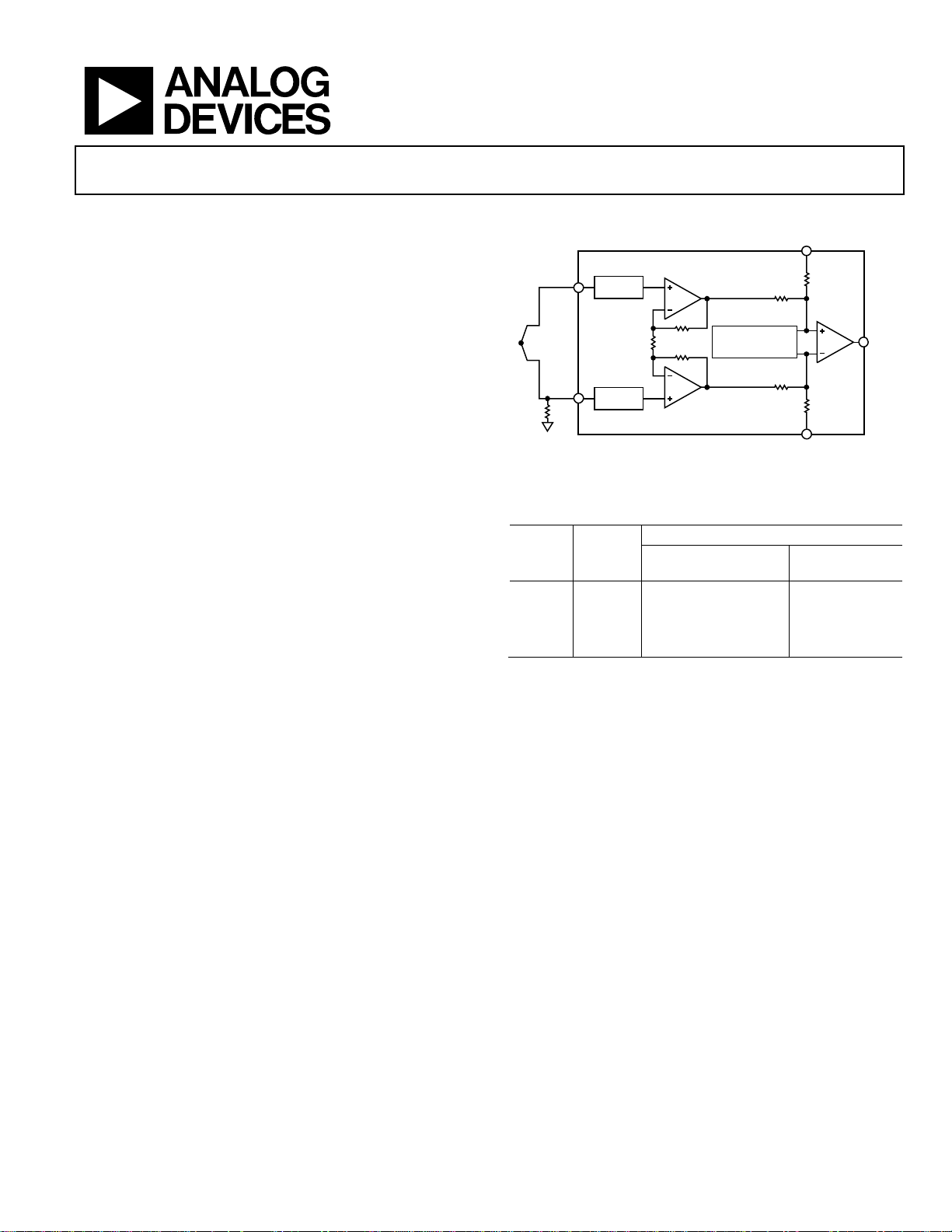
FUNCTIONAL BLOCK DIAGRAM
REF
AD8494/AD8495/
+IN
ESD AND
OVP
THERMOCOUPLE
–IN
ESD AND
1MΩ
OVP
Table 1. Device Temperature Ranges
ThermoCoupl e
Part No.
Typ e
AD8494 J 0°C to 50°C Full J type range
AD8495 K 0°C to 50°C Full K type range
AD8496 J 25°C to 100°C Full J type range
AD8497 K 25°C to 100°C Full K type range
AD8496/AD8497
A2
COLD JUNCTIO N
COMPENSATION
A1
SENSE
Figure 1.
Optimized Temperature Range
Ambient Temperature
(Reference Junction)
Measurement
Junction
A3
OUT
08529-001
GENERAL DESCRIPTION
The AD8494/AD8495/AD8496/AD8497 are precision
instrumentation amplifiers with thermocouple cold junction
compensators on an integrated circuit. They produce a high
level (5 mV/°C) output directly from a thermocouple signal by
combining an ice point reference with a precalibrated amplifier.
They can be used as standalone thermometers or as switched
output setpoint controllers using either a fixed or remote
setpoint control.
The AD8494/AD8495/AD8496/AD8497 can be powered from a
single-ended supply (less than 3 V) and can measure temperatures
below 0°C by offsetting the reference input. To minimize selfheating, an unloaded AD849x typically operates with a total
supply current of 180 µA, but it is also capable of delivering in
excess of ±5 mA to a load.
The AD8494 and AD8496 are precalibrated by laser wafer
trimming to match the characteristics of J type (iron-constantan)
thermocouples; the AD8495 and AD8497 are laser trimmed to
match the characteristics of K type (chromel-alumel) thermocouples. See Tabl e 1 for the optimized ambient temperature
range of each part.
Rev. C
Information furnished by Analog Devices is believed to be accurate and reliable. However, no
responsibility is assumed by Anal og Devices for its use, nor for any infringements of patents or ot her
rights of third parties that may result from its use. Specifications subject to change without notice. No
license is granted by implication or otherwise under any patent or patent rights of Analog Devices.
Trademarks and registered trademarks are the property of their respective owners.
The AD8494/AD8495/AD8496/AD8497 allow a wide variety of
supply voltages. With a 5 V single supply, the 5 mV/°C output
allows the devices to cover nearly 1000 degrees of a thermocouple’s temperature range.
The AD8494/AD8495/AD8496/AD8497 work with 3 V supplies,
allowing them to interface directly to lower supply ADCs. They
can also work with supplies as large as 36 V in industrial systems
that require a wide common-mode input range.
PRODUCT HIGHLIGHTS
1. Complete, precision laser wafer trimmed thermocouple
signal conditioning system in a single IC package.
2. Flexible pinout provides for operation as a setpoint
controller or as a standalone Celsius thermometer.
3. Rugged inputs withstand 4 kV ESD and provide over-
voltage protection (OVP) up to V
4. Differential inputs reject common-mode noise on the
thermocouple leads.
5. Reference pin voltage can be offset to measure 0°C on
single supplies.
6. Available in a small, 8-lead MSOP that is fully RoHS compliant.
One Technology Way, P.O. Box 9106, Norwood, MA 02062-9106, U.S.A.
Tel: 781.329.4700 www.analog.com
Fax: 781.461.3113 ©2010–2011 Analog Devices, Inc. All rights reserved.
± 25 V.
S
Page 2

AD8494/AD8495/AD8496/AD8497
TABLE OF CONTENTS
Features.............................................................................................. 1
Applications....................................................................................... 1
Functional Block Diagram .............................................................. 1
General Description ......................................................................... 1
Product Highlights ........................................................................... 1
Revision History ............................................................................... 2
Specifications..................................................................................... 3
Absolute Maximum Ratings............................................................ 5
Thermal Resistance ...................................................................... 5
ESD Caution.................................................................................. 5
Pin Configuration and Function Descriptions............................. 6
Typical Performance Characteristics ............................................. 7
Theory of Operation ...................................................................... 11
REVISION HISTORY
6/11—Rev. B to Rev. C
Changes to Figure 35 and Figure 36............................................. 15
4/11—Rev. A to Rev. B
Changes to Figure 1.......................................................................... 1
Changes to Figure 33 and Figure 34............................................. 14
Changes to Figure 35 and Figure 36............................................. 15
Changes to Ordering Guide.......................................................... 16
10/10—Rev. 0 to Rev. A
Changes to Linearity Error of the Thermocouple Section........ 12
Changes to Ambient Temperature Sensor Section .................... 14
Changes to Ordering Guide.......................................................... 16
7/10—Revision 0: Initial Version
Thermocouples........................................................................... 11
Thermocouple Signal Conditioner.......................................... 11
AD8494/AD8495/AD8496/AD8497 Architecture .................. 11
Maximum Error Calculation.................................................... 12
Recommendations for Best Circuit Performance .................. 13
Applications Information.............................................................. 14
Basic Connection ....................................................................... 14
Ambient Temperature Sensor................................................... 14
Setpoint Controller .................................................................... 15
Measuring Negative Temperatures .......................................... 15
Reference Pin Allows Offset Adjustment................................ 15
Outline Dimensions....................................................................... 16
Ordering Guide .......................................................................... 16
Rev. C | Page 2 of 16
Page 3

AD8494/AD8495/AD8496/AD8497
SPECIFICATIONS
+VS = 5 V, −VS = 0 V, V
gain and offset errors of the thermocouple itself. T
temperature; T
is the thermocouple measurement junction temperature.
MJ
Table 2.
A Grade C Grade
Parameter Test Conditions/Comments Min Typ Max Min Typ Max Unit
TEMPERATURE ACCURACY
Initial Accuracy
AD8494/AD8495 TA = TRJ = TMJ = 25°C 3 1 °C
AD8496/AD8497 TA = TRJ = 60°C, TMJ = 175°C 3 1.5 °C
Ambient Temperature
Rejection
1
AD8494/AD8495 TA = TRJ = 0°C to 50°C 0.05 0.025 °C/°C
AD8496/AD8497 TA = TRJ = 25°C to 100°C 0.05 0.025 °C/°C
Gain Error2, 3 V
AD8494/AD8495 0.3 0.1 %
AD8496/AD8497 0.3 0.1 %
Transfer Function 5 5 mV/°C
INPUTS
Input Voltage Range −VS – 0.2 +VS – 1.6 −VS – 0.2 +VS – 1.6 V
Overvoltage Range +VS – 25 −VS + 25 +VS – 25 −VS + 25 V
Input Bias Current4 25 50 25 50 nA
Input Offset Current 1.5 0.5 nA
Common-Mode Rejection VCM = 0 V to 3 V 1 0.3 °C/V
Power Supply Rejection +VS = 2.7 V to 5 V 0.5 0.5 °C/V
NOISE
Voltage Noise f = 0.1 Hz to 10 Hz, TA = 25°C 0.8 0.8 μV p-p
Voltage Noise Density f = 1 kHz, TA = 25°C 32 32 nV/√Hz
Current Noise Density f = 1 kHz, TA = 25°C 100 100 fA/√Hz
REFERENCE INPUT
Input Resistance 60 60 kΩ
Input Current 25 25 μA
Voltage Range −VS +VS −VS +VS V
Gain to Output 1 1 V/V
OUTPUT
Output Voltage Range −VS + 0.025 +VS – 0.1 −VS + 0.025 +VS – 0.1 V
Short-Circuit Current5 7 7 mA
DYNAMIC RESPONSE
−3 dB Bandwidth
AD8494 30 30 kHz
AD8495/AD8497 25 25 kHz
AD8496 31 31 kHz
Settling Time to 0.1% 4 V output step
AD8494 36 36 μs
AD8495/AD8497 40 40 μs
AD8496 32 32 μs
POWER SUPPLY
Operating Voltage Range6
Single Supply 2.7 36 2.7 36 V
Dual Supply ±2.7 ±18 ±2.7 ±18 V
Quiescent Current 180 250 180 250 μA
+IN
= V
= 0 V, V
−IN
= 0 V, TA = TRJ = 25°C, RL = 100 k, unless otherwise noted. Specifications do not include
REF
is the ambient temperature at the AD849x; TRJ is the thermocouple reference junction
A
= 0.125 V to 4.125 V
OUT
Rev. C | Page 3 of 16
Page 4

AD8494/AD8495/AD8496/AD8497
A Grade C Grade
Parameter Test Conditions/Comments Min Typ Max Min Typ Max Unit
TEMPERATURE RANGE (TA)
Specified Performance
AD8494/AD8495 0 50 0 50 °C
AD8496/AD8497 25 100 25 100 °C
Operational −40 +125 −40 +125 °C
1
Ambient temperature rejection specifies the change in the output measurement (in °C) for a given change in temperature of the cold junction. For the AD8494 and
AD8495, ambient temperature rejection is defined as the slope of the line connecting errors calculated at 0°C and 50°C ambient temperature. For the AD8496 and
AD8497, ambient temperature rejection is defined as the slope of the line connecting errors calculated at 25°C and 100°C ambient temperature.
2
Error does not include thermocouple gain error or thermocouple nonlinearity.
3
With a 100 kΩ load, measurement junction temperatures beyond approximately 880°C for the AD8494 and AD8496 and beyond approximately 960°C for the AD8495
and AD8497 require supply voltages larger than 5 V or a negative voltage applied to the reference pin. Measurement junction temperatures below 5°C require either a
positive offset voltage applied to the reference pin or a negative supply.
4
Input stage uses PNP transistors, so bias current always flows out of the part.
5
Large output currents can increase the internal temperature rise of the part and contribute to cold junction compensation (CJC) error.
6
Unbalanced supplies can also be used. Care should be taken that the common-mode voltage of the thermocouple stays within the input voltage range of the part.
Rev. C | Page 4 of 16
Page 5

AD8494/AD8495/AD8496/AD8497
ABSOLUTE MAXIMUM RATINGS
Table 3.
Parameter Rating
Supply Voltage ±18 V
Maximum Voltage at −IN or +IN +VS – 25 V
Minimum Voltage at −IN or +IN –VS + 25 V
REF Voltage ±VS
Output Short-Circuit Current Duration Indefinite
Storage Temperature Range −65°C to +150°C
Operating Temperature Range −40°C to +125°C
Maximum IC Junction Temperature 140°C
ESD
Human Body Model 4.5 kV
Field-Induced Charged Device Model 1.5 kV
Stresses above those listed under Absolute Maximum Ratings
may cause permanent damage to the device. This is a stress
rating only; functional operation of the device at these or any
other conditions above those indicated in the operational
section of this specification is not implied. Exposure to absolute
maximum rating conditions for extended periods may affect
device reliability.
THERMAL RESISTANCE
θJA is specified for a device on a 4-layer JEDEC PCB in free air.
Table 4.
Package θJA Unit
8-Lead MSOP (RM-8) 135 °C/W
ESD CAUTION
Rev. C | Page 5 of 16
Page 6

AD8494/AD8495/AD8496/AD8497
PIN CONFIGURATION AND FUNCTION DESCRIPTIONS
AD849x
1
–IN
REF
–V
NC
S
–
2
3
4
TOP VIEW
(Not to Scale)
NC = NO CONNECT
Figure 2. Pin Configuration
Table 5. Pin Function Descriptions
Pin No. Mnemonic Description
1 −IN Negative Input.
2 REF Reference. This pin must be driven by low impedance.
3 −VS Negative Supply.
4 NC No Connect.
5 SENSE Sense Pin. In measurement mode, connect to output; in setpoint mode, connect to setpoint voltage.
6 OUT Output.
7 +VS Positive Supply.
8 +IN Positive Input.
8
7
6
5
+IN
+V
S
OUT
SENSE
08529-002
+
Rev. C | Page 6 of 16
Page 7

AD8494/AD8495/AD8496/AD8497
TYPICAL PERFORMANCE CHARACTERISTICS
TA = 25°C, +VS = 5 V, RL = ∞, unless otherwise noted.
100
10
AD8495/AD8497
AD8494
AD8496
1200
1000
800
CONNECTED
THERMOCOUPL E
1
CMRR (°C/V)
0.1
0.01
0.1 1 10 100 1k 10k 100k
FREQUENCY (Hz)
Figure 3. CMRR vs. Frequency
1000
PSRR (°C/V)
AD8495/AD8497
AD8494
AD8496
100
10
1
0
1 10 100 1k 10k 100k
FREQUENCY (Hz)
Figure 4. PSRR vs. Frequency
600
400
200
TEMPE RATURE RE ADING (°C)
0
THERMOCOUPL E CONNECTION
–200
08529-035
AD849x OUTPUT
TIME (50µ s/DIV)
OPEN THERMOCOUPLE
08529-019
Figure 6. Output Response to Open Thermocouple,
−IN Connected to Ground Through a 1 MΩ Resistor
4.0
+0.05, +3.45
3.5
3.0
+0.05, +3.21
2.5
2.0
1.5
1.0
0.5
0
INPUT COMMON-MODE VOLTAGE (V)
–0.5
–1.0
08529-036
+0.05, –0.36
V
+0.05, –0.39
–0.5 0.5 1. 5 2.5 3.5 4.5 5.5
OUTPUT VOLTAGE (V)
= 0V
REF
= 2.5V
V
REF
+4.91, +2.95
+4.91, +2.71
+4.91, –0.37
+4.91, –0.39
08529-017
Figure 7. Input Common-Mode Voltage Range vs. Output Voltage,
+V
= 5 V, V
S
= 0 V, and V
REF
= 2.5 V
REF
50
40
30
20
10
GAIN (dB)
0
–10
–20
100 1k 10k 100k 1M
AD8494
AD8496
AD8495/AD8497
FREQUENCY (Hz)
Figure 5. Frequency Response
08529-018
Rev. C | Page 7 of 16
40
35
30
25
20
15
10
INPUT BIAS CURRENT (nA)
5
0
–40 –20 0 20 40 60 80 100 120
TEMPERATURE (° C)
I
BIAS
I
OS
2.00
1.75
1.50
1.25
1.00
0.75
0.50
0.25
0
Figure 8. Input Bias Current and Input Offset Current vs. Temperature
INPUT OFFSET CURRENT ( nA)
08529-042
Page 8

AD8494/AD8495/AD8496/AD8497
3.00
2.75
2.50
2.25
2.00
1.75
1.50
1.25
1.00
OUTPUT VOLTAGE (V)
0.75
0.50
0.25
0
–30 –10 –5 0 5 15 20 25–25 –20 –15 10 30
V
OUT
I
IN
INPUT VOLTAGE (V)
Figure 9. AD8494 Input Overvoltage Performance, +V
2.00
1.50
1.00
0.50
0
–0.50
–1.00
= 2.7 V (Gain = 96.7)
S
INPUT CURRENT (mA)
08529-021
16
12
8
4
0
–4
OUTPUT VOLTAGE (V)
–8
–12
–16
–30 –10 –5 0 5 15 20 25–25 –20 –15 10 30
V
OUT
INPUT VOLTAGE (V)
I
IN
Figure 12. AD8494 Input Overvoltage Performance, V
3.0
2.5
2.0
1.5
1.0
0.5
INPUT CURRENT (mA)
0
–0.5
–1.0
= ±15 V (Gain = 96.7)
S
08529-024
3.00
2.75
2.50
2.25
2.00
1.75
1.50
1.25
1.00
OUTPUT VO LTAGE (V )
0.75
0.50
0.25
0
–30 –10 –5 0 5 15 20 25–25 –20 –15 10 30
V
OUT
I
IN
INPUT VOLTAGE (V)
Figure 10. AD8495/AD8497 Input Overvoltage Performance,
= 2.7 V (Gain = 122.4)
+V
S
3.00
2.75
2.50
2.25
2.00
1.75
1.50
1.25
1.00
OUTPUT VO LTAGE (V )
0.75
0.50
0.25
0
–30 –10 –5 0 5 15 20 25–25 –20 –15 10 30
V
OUT
I
IN
INPUT VOLTAGE (V)
Figure 11. AD8496 Input Overvoltage Performance, +V
Gain = 90.35)
= 2.7 V
S
2.00
1.50
1.00
0.50
0
–0.50
–1.00
2.00
1.50
1.00
0.50
0
–0.50
–1.00
16
12
8
4
0
–4
INPUT CURRENT (mA)
08529-022
OUTPUT VOLTAGE (V)
–8
–12
–16
–30 –10 –5 0 5 15 20 25–25 –20 –15 10 30
V
OUT
INPUT VOLTAGE (V)
I
IN
3.0
2.5
2.0
1.5
1.0
0.5
0
–0.5
–1.0
INPUT CURRENT (mA)
08529-025
Figure 13. AD8495/AD8497 Input Overvoltage Performance,
= ±15 V (Gain = 122.4)
V
S
16
12
8
4
0
–4
INPUT CURRENT (mA)
08529-023
OUTPUT VOLTAGE (V)
–8
–12
–16
–30 –10 –5 0 5 15 20 25–25 –20 –15 10 30
Figure 14. AD8496 Input Overvoltage Performance, V
V
OUT
INPUT VOLTAGE (V)
I
IN
= ±15 V (Gain = 90.35)
S
3.0
2.5
2.0
1.5
1.0
0.5
0
–0.5
–1.0
INPUT CURRENT (mA)
08529-026
Rev. C | Page 8 of 16
Page 9

AD8494/AD8495/AD8496/AD8497
V
V
V
CL = 0pF
C
= 1000pF
L
CL = 0pF
C
= 1000pF
L
20mV/DI
120µs/DIV
Figure 15. AD8494/AD8496 Small-Signal Response
with Various Capacitive Loads
AD8494/AD8496
AD8495/AD8497
20mV/DI
120µs/DIV
Figure 16. Small-Signal Response, R
= 100 kΩ, CL = 1 nF
L
CL = 4700pF
C
= 10000pF
L
20mV/DI
CL = 4700pF
C
= 10000pF
L
08529-028
120µs/DIV
08529-029
Figure 18. AD8495/AD8497 Small-Signal Response
with Various Capacitive Loads
2V/DIV
0.02%/DIV
08529-027
SETTL ING TO 0.1% IN 36µs
100µs/DIV
08529-039
Figure 19. AD8494 Large-Signal Step Response and Settling Time
2V/DIV
0.02%/DIV
SETTLING TO 0.1% IN 40µs
100µs/DIV
08529-040
Figure 17. AD8495/AD8497 Large-Signal Step Response and Settling Time
2V/DIV
0.02%/DIV
SETTL ING TO 0.1% IN 32µs
100µs/DIV
08529-041
Figure 20. AD8496 Large-Signal Step Response and Settling Time
Rev. C | Page 9 of 16
Page 10

AD8494/AD8495/AD8496/AD8497
V
V
OUTPUT VOLTAGE
5V POWER-UP
(1.25V/DIV)
SUPPLY VOLTAGE
200nV/DI
(50mV/DIV)
OUTPUT VOLTAGE
1s/DIV
Figure 21. 0.1 Hz to 10 Hz RTI Voltage Noise
5
4
3
2
1
0
–1
–2
OUTPUT VOL TAGE SWING (V)
–3
–4
–5
1k 10k 100k
LOAD RESISTANCE (Ω)
Figure 22. Output Voltage Swing vs. Load Resistance, V
100
90
80
70
60
50
NOISE (nV / Hz)
40
30
20
10
1 10 100 1k 10k 100k
FREQUENCY (Hz)
Figure 23. Voltage Noise Spectral Density vs. Frequency
(+) –40°C
(+) +25°C
(+) +85°C
(+) +125°C
(–) –40°C
(–) +25°C
(–) +85°C
(–) +125°C
= ±5 V
S
08529-030
TIME (1.5ms/DIV)
08529-032
Figure 24. Output Voltage Start-Up
+
S
–0.4
= ±5V)
–0.8
S
–1.2
+1.2
OUTPUT VOLTAGE SWING (V)
+0.8
+0.4
REFERRED TO SUPPLY VOLTAGES (V
–V
08529-033
Figure 25. Output Voltage Swing vs. Output Current, V
(+) –40°C
(+) +25°C
(+) +85°C
(+) +125°C
(–) –40°C
(–) +25°C
(–) +85°C
(–) +125°C
S
10µ 100µ 1m 5m
OUTPUT CURRENT (A)
= ±5 V
S
08529-034
08529-031
Rev. C | Page 10 of 16
Page 11

AD8494/AD8495/AD8496/AD8497
THEORY OF OPERATION
THERMOCOUPLES
A thermocouple is a rugged, low cost temperature transducer
whose output is proportional to the temperature difference
between a measurement junction and a reference junction. It
has a very wide temperature range. Its low level output (typically
tens of microvolts per °C) requires amplification. Variation in
the reference junction temperature results in measurement
error unless the thermocouple signal is properly compensated.
A thermocouple consists of two dissimilar metals. These metals
are connected at one end to form the measurement junction,
also called the hot junction. The other end of the thermocouple
is connected to the metal lines that lead to the measurement
electronics. This connection forms a second junction: the
reference junction, also called the cold junction.
MEASUREMENT
JUNCTION
REFERENCE
JUNCTION
PCB
TRACES
AD849x
Table 6. J Type Thermocouple Voltages and AD8494 Readings
Measurement
Junction
Temperature
)
(T
MJ
Reference
Junction
Temperature
)
(T
RJ
Thermocouple
Voltage
AD8494
Reading
50°C 0°C +2.585 mV 250 mV
50°C 50°C 0 mV 250 mV
0°C 0°C 0 mV 0 mV
0°C 50°C −2.585 mV 0 mV
AD8494/AD8495/AD8496/AD8497 ARCHITECTURE
Figure 27 shows a block diagram of the AD849x circuitry. The
AD849x consists of a low offset, fixed-gain instrumentation
amplifier and a temperature sensor.
REF
AD8494/AD8495/
+IN
ESD AND
OVP
AD8496/AD8497
A2
THERMO COUPL E WIR ES
Figure 26. Thermocouple Junctions
08529-004
To derive the temperature at the measurement junction (TMJ),
the user must know the differential voltage created by the thermocouple. The user must also know the error voltage generated by
the temperature at the reference junction (T
). Compensating
RJ
for the reference junction error voltage is typically called cold
junction compensation. The electronics must compensate for
any changes in temperature at the reference (cold) junction so
that the output voltage is an accurate representation of the hot
junction measurement.
THERMOCOUPLE SIGNAL CONDITIONER
The AD8494/AD8495/AD8496/AD8497 thermocouple amplifiers
provide a simple, low cost solution for measuring thermocouple
temperatures. These amplifiers simplify many of the difficulties
of measuring thermocouples. An integrated temperature sensor
performs cold junction compensation. A fixed-gain instrumentation
amplifier amplifies the small thermocouple voltage to provide a
5 mV/°C output. The high common-mode rejection of the
amplifier blocks common-mode noise that the long thermocouple
leads can pick up. For additional protection, the high impedance
inputs of the amplifier make it easy to add extra filtering.
Tabl e 6 shows an example of a J type thermocouple voltage for
various combinations of 0°C and 50°C on the reference and
measurement junctions. Ta ble 6 also shows the performance
of the AD8494 amplifying the thermocouple voltage and
compensating for the reference junction temperature changes,
thus eliminating the error.
A1
COLD JUNCTIO N
COMPENSATION
SENSE
A3
OUT
THERMOCOUPLE
–IN
1MΩ
ESD AND
OVP
Figure 27. Block Diagram
The AD849x output is a voltage that is proportional to the temperature at the measurement junction of the thermocouple (T
).
MJ
To derive the measured temperature from the AD849x output
voltage, use the following transfer function:
T
MJ
= (V
OUT
− V
REF
)/(5 mV/°C)
An ideal AD849x achieves this output with an error of less than
±2°C, within the specified operating ranges listed in Tabl e 7.
Instrumentation Amplifier
A thermocouple signal is so small that considerable gain is
required before it can be sampled properly by most ADCs. The
AD849x has an instrumentation amplifier with a fixed gain that
generates an output voltage of 5 mV/°C for J type and K type
thermocouples.
V
= (TMJ × 5 mV/°C) + V
OUT
REF
To accommodate the nonlinear behavior of the thermocouple,
each amplifier has a different gain so that the 5 mV/°C is accurately maintained for a given temperature measurement range.
• The AD8494 and AD8496 (J type) have an instrumentation
amplifier with a gain of 96.7 and 90.35, respectively.
• The AD8495 and AD8497 (K type) have an instrumentation
amplifier with a gain of 122.4.
08529-020
Rev. C | Page 11 of 16
Page 12

AD8494/AD8495/AD8496/AD8497
The small thermocouple voltages mean that signals are quite
vulnerable to interference, especially when measured with
single-ended amplifiers. The AD849x addresses this issue in
several ways. Low input bias currents and high input impedance
allow for easy filtering at the inputs. The excellent common-mode
rejection of the AD849x prevents variations in ground potential
and other common-mode noise from affecting the measurement.
Temperature Sensor (Cold Junction Compensation)
The AD849x also includes a temperature sensor for cold junction compensation. This temperature sensor is used to measure
the reference junction temperature of the thermocouple and to
cancel its effect.
• The AD8494/AD8495 cold junction compensation is
optimized for operation in a lab environment, where the
ambient temperature is around 25°C. The AD8494/AD8495
are specified for an ambient range of 0°C to 50°C.
• The AD8496/AD8497 cold junction compensation is
optimized for operation in a less controlled environment,
where the temperature is around 60°C. The AD8496/AD8497
are specified for an ambient range of 25°C to 100°C.
Application examples for the AD8496/AD8497 include
automotive applications, autoclave, and ovens.
Thermocouple Break Detection
The AD849x offers open thermocouple detection. The inputs
of the AD849x are PNP type transistors, which means that the
bias current always flows out of the inputs. Therefore, the input
bias current drives any unconnected input high, which rails the
output. Connecting the negative input to ground through a
1 MΩ resistor causes the AD849x output to rail high in an open
thermocouple condition (see Figure 6, Figure 28, and the
Ground Connection section).
1MΩ
08529-008
Figure 28. Ground the Negative Input Through a 1 MΩ Resistor
for Open Thermocouple Detection
Input Voltage Protection
The AD849x has very robust inputs. Input voltages can be up
to 25 V from the opposite supply rail. For example, with a +5 V
positive supply and a −3 V negative supply, the part can safely
withstand voltages at the inputs from −20 V to +22 V. Voltages
at the reference and sense pins should not go beyond 0.3 V of
the supply rails.
MAXIMUM ERROR CALCULATION
As is normally the case, the AD849x outputs are subject to
calibration, gain, and temperature sensitivity errors. The user
can calculate the maximum error from the AD849x using the
following information.
The five primary sources of AD849x error are described in this
section.
AD849x Initial Calibration Accuracy
Error at the initial calibration point can be easily calibrated out
with a one-point temperature calibration. See Tab l e 2 for the
specifications.
AD849x Ambient Temperature Rejection
The specified ambient temperature rejection represents the
ability of the AD849x to reject errors caused by changes in the
ambient temperature/reference junction. For example, with
0.025°C/°C ambient temperature rejection, a 20°C change in the
reference junction temperature adds less than 0.5°C error to the
measurement. See Tab le 2 for the specifications.
AD849x Gain Error
Gain error is the amount of additional error when measuring away
from the measurement junction calibration point. For example,
if the part is calibrated at 25°C and the measurement junction is
100°C with a gain error of 0.1%, the gain error contribution is
(100°C − 25°C) × (0.1%) = 0.075°C. This error can be calibrated
out with a two-point calibration if needed, but it is usually small
enough to ignore. See Tab l e 2 for the specifications.
Manufacturing Tolerances of the Thermocouple
Consult the data sheet for your thermocouple to find the
specified tolerance of the thermocouple.
Linearity Error of the Thermocouple
Each part in the AD849x family is precision trimmed to optimize
a linear operating range for a specific thermocouple type and
for the widest possible measurement and ambient temperature
ranges. The AD849x achieves a linearity error of less than ±2°C,
within the specified operating ranges listed in Tabl e 7. This error
is due only to the nonlinearity of the thermocouple.
Table 7. AD849x ±2°C Accuracy Temperature Ranges
Thermocouple
Part
AD8494 J ±2°C 0°C to 50°C −35°C to +95°C
AD8495 K ±2°C 0°C to 50°C −25°C to +400°C
AD8496 J ±2°C 25°C to 100°C +55°C to +565°C
AD8497 K ±2°C 25°C to 100°C −25°C to +295°C
Typ e
Max
Error
For temperature ranges outside those listed in Ta b le 7 or for
instructions on how to correct for thermocouple nonlinearity
error with software, see the AN-1087 Application Note for
additional details.
Ambient
Temperature
Range
Measurement
Temperature
Range
Rev. C | Page 12 of 16
Page 13

AD8494/AD8495/AD8496/AD8497
RECOMMENDATIONS FOR BEST CIRCUIT PERFORMANCE
Input Filter
A low-pass filter before the input of the AD849x is strongly
recommended (see Figure 29), especially when operating in an
electrically noisy environment. Long thermocouple leads can
function as an excellent antenna and pick up many unwanted
signals.
The filter should be set to a low corner frequency that still
allows the input signal to pass through undiminished. The
primary purpose of the filter is to remove RF signals, which,
if allowed to reach the AD849x, can be rectified and appear
as temperature fluctuations.
Keeping the AD849x at the Same Temperature as the Reference Junction
The AD849x compensates for thermocouple reference junction
temperature by using an internal temperature sensor. It is
critical to keep the reference junction (thermocouple-to-PCB
connection) as close to the AD849x as possible. Any difference
in temperature between the AD849x and the reference junction
appears directly as temperature error. Temperature difference
between the device and the reference junction may occur if the
AD849x is not physically close to the reference junction or if the
AD849x is required to supply large amounts of output power.
KEEP JUNCTION AND
MEASUREMENT
JUNCTION
REFERENCE
JUNCTION
AD849x AT SAME
TEMPERATURE
C
C
R
C
D
R
CONNECT WHEN
THERMOCOUPL E TIP
TYPE IS UNKNO WN
FILTER FREQUENCY
FILTER FREQUENCYCM =
WHERE C
≥ 10C
D
1MΩ
C
=
DIFF
2πR(2C
2πRC
C
AD849x
C
1
+ CC)
D
1
C
08529-011
Figure 29. Filter for Any Thermocouple Style
To prevent input offset currents from affecting the measurement
accuracy, the filter resistor values should be less than 50 k.
Ground Connection
It is always recommended that the thermocouple be connected
to ground through a 100 k to 1 M resistor placed at the
negative (inverting) input of the amplifier on the PCB (see
Figure 30). This solution works well regardless of the thermocouple tip style.
1MΩ
08529-038
Figure 30. Ground the Thermocouple with a 1 MΩ Resistor
If there is no electrical connection at the measurement junction
(insulated tip), the resistor value is small enough that no meaningful common-mode voltage is generated. If there is an electrical
connection through a grounded or exposed tip, the resistor value
is large enough that any current from the measurement tip to
ground is very small, preventing measurement errors.
The AD849x inputs require only one ground connection or source
of common-mode voltage. Any additional ground connection is
detrimental to performance because ground loops can form
through the thermocouple, easily swamping the small
thermocouple signal. Grounding the thermocouple through a
resistor as recommended prevents such problems.
THERMOCOUPL E WIRES
PCB
TRACES
KEEP
TRACES
SHORT
AD849x
08529-010
Figure 31. Compensating for Thermocouple Reference Junction Temperature
Driving the Reference Pin
The AD849x comes with a reference pin, which can be used
to offset the output voltage. This is particularly useful when
reading a negative temperature in a single-supply system.
INCORRECT
AD849x
REF
V
Figure 32. Driving the Reference Pin
V
CORRECT
+
AD8613
–
AD849x
REF
08529-006
For best performance, the reference pin should be driven with a
low output impedance source, not a resistor divider. The AD8613
and the OP777 are good choices for the buffer amplifier.
Debugging Tip
If the AD849x is not providing the expected performance, a
useful debugging step is to implement the ambient temperature
configuration in Figure 34. If the ambient temperature sensor
does not work as expected, the problem is likely with the AD849x
or with the downstream circuitry. If the ambient temperature
sensor configuration is working correctly, the problem typically
lies with how the thermocouple is connected to the AD849x.
Common errors include an incorrect grounding configuration
or lack of filtering.
Rev. C | Page 13 of 16
Page 14

AD8494/AD8495/AD8496/AD8497
V
V
APPLICATIONS INFORMATION
BASIC CONNECTION
Figure 33 shows an example of a basic connection for the
AD849x, with a J type or K type thermocouple input.
5
0.1µF 10µF
+V
S
7
COLD JUNCTIO N
COMPENSATION
+IN
THERMO-
COUPLE
1MΩ
–IN
8
IN-AMP
1
AD849x
2 3
REF
–V
S
Figure 33. Basic Connection for the AD849x
To measure negative temperatures, apply a voltage at the reference pin to offset the output voltage at 0°C. The output voltage
of the AD849x is
V
= (TMJ × 5 mV/°C) + V
OUT
REF
A filter at the input is recommended to remove high frequency
noise. The 1 M resistor to ground enables open thermocouple
detection and proper grounding of the thermocouple. The sense
pin should be connected to the output pin of the AD849x.
Decoupling capacitors should be used to ensure clean power
supply voltages on +V
and, if using dual supplies, on −VS, also.
S
A 0.1 µF capacitor should be placed as close as possible to each
AD849x supply pin. A 10 µF tantalum capacitor can be used
farther away from the part and can be shared.
SENSE
5
6
OUT
0.1µF 10µF
08529-012
AMBIENT TEMPERATURE SENSOR
The AD849x can be configured as a standalone Celsius thermometer with a 5 mV/°C output, as shown in Figure 34. The
thermocouple sensing functionality is disabled by shorting both
AD849x inputs to ground; the AD849x simply outputs the value
from the on-board temperature sensor.
As a temperature sensor, the AD8494 has a measurement temperature range of −40°C to +125°C with a precision output of
V
= TA × 5 mV/°C
OUT
5
+V
S
7
COLD JUNCTION
COMPENSATI ON
+IN
8
–IN
IN-AMP
1
AD849x
2 3
REF –V
Figure 34. Ambient Temperature Sensor
The AD8494 is the best choice for use as an ambient temperature sensor. The AD8495, AD8496, and AD8497 can also be
configured as ambient temperature sensors, but their output
transfer functions are not precisely 5 mV/°C. For information
about the exact transfer functions of the AD8494/AD8495/
AD8496/AD8497, see the AN-1087 Application Note for
additional details.
The thermometer mode can be particularly useful for debugging
a misbehaving circuit. If the basic connection is not working,
disconnect the thermocouple and short both inputs to ground.
If the system reads the ambient temperature correctly, the
problem is related to the thermocouple. If the system does not
read the ambient temperature correctly, the problem is with
the AD849x or with the downstream circuitry.
SENSE
5
6
OUT
S
08529-013
Rev. C | Page 14 of 16
Page 15

AD8494/AD8495/AD8496/AD8497
V
SETPOINT CONTROLLER
The AD849x can be used as a temperature setpoint controller,
with a thermocouple input from a remote location or with the
AD849x itself being used as a temperature sensor. When the
measured temperature is below the setpoint temperature, the
output voltage goes to −V
above the setpoint temperature, the output voltage goes to +V
For best accuracy and CMRR performance, the setpoint voltage
should be created with a low impedance source. If the setpoint
voltage is generated with a voltage divider, a buffer is
recommended.
+IN
THERMO-
COUPLE
1MΩ
–IN
Hysteresis can be added to the setpoint controller by using a
resistor divider from the output to the reference pin, as shown
in Figure 36. The hysteresis in °C is
. When the measured temperature is
S
5
+V
S
7
COLD JUNCTION
COMPENSATIO N
8
IN-AMP
1
6
5
OUT
SENSE
AD849x
2 3
REF
–V
S
Figure 35. Setpoint Controller
SETPOINT
VOLTAGE
S
.
08529-014
MEASURING NEGATIVE TEMPERATURES
The AD849x can measure negative temperatures on dual
supplies and on a single supply. When operating on dual
supplies with the reference pin grounded, a negative output
voltage indicates a negative temperature at the thermocouple
measurement junction.
= (TMJ × 5 mV/°C) + V
V
OUT
REF
When operating the AD849x on a single supply, level-shift
the output by applying a positive voltage (less than +V
the reference pin. An output voltage less than V
indicates
REF
) on
S
a negative temperature at the thermocouple measurement
junction.
REFERENCE PIN ALLOWS OFFSET ADJUSTMENT
The reference pin can be used to level-shift the AD849x output
voltage. This is useful for measuring negative temperatures on a
single supply and to match the AD849x output voltage range to
the input voltage range of the subsequent electronics in the
signal chain.
The reference pin can also be used to offset any initial calibration errors. Apply a small reference voltage proportional to the
error to nullify the effect of the calibration error on the output.
)/(°+×
T
HYST
THERMO-
COUPLE
1MΩ
S
=
+IN
–IN
R2R1R1V
CmV/5
COLD JUNCTIO N
COMPENSATION
8
IN-AMP
1
2 3
REF
R1
1kΩ
AD849x
100kΩ
5V
+V
S
7
OUT
6
SENSE
5
–V
S
R2
R1
1kΩ
SETPOINT
VOLTAGE
Figure 36. Adding 10 Degrees of Hysteresis
A resistor equivalent to the output resistance of the divider should
be connected to the sense pin to ensure good CMRR.
08529-015
Rev. C | Page 15 of 16
Page 16

AD8494/AD8495/AD8496/AD8497
OUTLINE DIMENSIONS
3.20
3.00
2.80
8
5
3.20
3.00
2.80
PIN 1
IDENTIFIER
0.95
0.85
0.75
0.15
0.05
COPLANARITY
1
0.65 BSC
0.10
COMPLIANT TO JEDEC STANDARDS MO-187-AA
Figure 37. 8-Lead Mini Small Outline Package [MSOP]
5.15
4.90
4.65
4
15° MAX
6°
0°
0.23
0.09
0.40
0.25
1.10 MAX
(RM-8)
Dimensions shown in millimeters
0.80
0.55
0.40
10-07-2009-B
ORDERING GUIDE
1
Model
AD8494ARMZ −40°C to +125°C 8-Lead MSOP RM-8 Y36
AD8494ARMZ-R7 −40°C to +125°C 8-Lead MSOP, 7” Tape and Reel RM-8 Y36
AD8494CRMZ −40°C to +125°C 8-Lead MSOP RM-8 Y37
AD8494CRMZ-R7 −40°C to +125°C 8-Lead MSOP, 7” Tape and Reel RM-8 Y37
AD8495ARMZ −40°C to +125°C 8-Lead MSOP RM-8 Y33
AD8495ARMZ-R7 −40°C to +125°C 8-Lead MSOP, 7” Tape and Reel RM-8 Y33
AD8495CRMZ −40°C to +125°C 8-Lead MSOP RM-8 Y34
AD8495CRMZ-R7 −40°C to +125°C 8-Lead MSOP, 7” Tape and Reel RM-8 Y34
AD8496ARMZ −40°C to +125°C 8-Lead MSOP RM-8 Y3C
AD8496ARMZ-R7 −40°C to +125°C 8-Lead MSOP, 7” Tape and Reel RM-8 Y3C
AD8496CRMZ −40°C to +125°C 8-Lead MSOP RM-8 Y3D
AD8496CRMZ-R7 −40°C to +125°C 8-Lead MSOP, 7” Tape and Reel RM-8 Y3D
AD8497ARMZ −40°C to +125°C 8-Lead MSOP RM-8 Y39
AD8497ARMZ-R7 −40°C to +125°C 8-Lead MSOP, 7” Tape and Reel RM-8 Y39
AD8497CRMZ −40°C to +125°C 8-Lead MSOP RM-8 Y3A
AD8497CRMZ-R7 −40°C to +125°C 8-Lead MSOP, 7” Tape and Reel RM-8 Y3A
1
Z = RoHS Compliant Part.
Temperature Range Package Description Package Option Branding
©2010–2011 Analog Devices, Inc. All rights reserved. Trademarks and
registered trademarks are the property of their respective owners.
D08529-0-6/11(C)
Rev. C | Page 16 of 16
 Loading...