ANALOG DEVICES AD8475 Service Manual

Precision, Selectable Gain,
FEATURES
Precision attenuation: G = 0.4, G = 0.8
Fully differential or single-ended input/output
Differential output designed to drive precision ADCs
Drives switched capacitor and Σ-Δ ADCs
Rail-to-rail output
VOCM pin adjusts output common mode
Robust overvoltage protection up to ±15 V (V
Single supply: 3 V to 10 V
Dual supplies: ±1.5 V to ±5 V
High performance
Suited for driving 18-bit converter up to 4 MSPS
10 nV/√Hz output noise
3 ppm/°C gain drift
500 μV maximum output offset
50 V/μs slew rate
Low power: 3.2 mA supply current
APPLICATIONS
ADC drivers
Differential instrumentation amplifier building blocks
Single-ended-to-differential converters
GENERAL DESCRIPTION
The AD8475 is a fully differential, attenuating amplifier with
integrated precision gain resistors. It provides precision attenuation
(by 0.4 or 0.8), common-mode level shifting, and single-ended-todifferential conversion along with input overvoltage protection.
Power dissipation on a single 5 V supply is only 16 mW.
The AD8475 is a simple to use, fully integrated precision gain
block, designed to process signal levels of up to ±10 V on a single
supply. It provides a complete interface to make industrial level
signals directly compatible with the differential input ranges of low
voltage high performance 16-bit or 18-bit single-supply successive
approximation (SAR) analog-to-digital converters (ADCs).
The AD8475 comes with two standard pin-selectable gain
options: 0.4 and 0.8. The gain of the part is set by driving the
input pin corresponding to the appropriate gain.
The AD8475 also provides overvoltage protection from large
industrial input voltages up to ±15 V while operating on a single
5 V supply. The VOCM pin adjusts the output voltage common
mode for precision level shifting, to match the ADC’s input range
and maximize dynamic range.
Rev. B
Information furnished by Analog Devices is believed to be accurate and reliable. However, no
responsibility is assumed by Anal og Devices for its use, nor for any infringements of patents or ot her
rights of third parties that may result from its use. Specifications subject to change without notice. No
license is granted by implication or otherwise under any patent or patent rights of Analog Devices.
Trademarks and registered trademarks are the property of their respective owners.
= +5 V)
S
Fully Differential Funnel Amplifier
AD8475
FUNCTIONAL BLOCK DIAGRAMS
S
S
S
–V
–V
–V
+IN 0.4x
16
+IN 0.4x
1
1.25kΩ
+IN 0.8x
2
–IN 0.8x
3
–IN 0.4x
NC = NO CONNECT
1.25kΩ
4
5
N 0.4x
–I
Figure 1. 16-Lead LFCSP
+IN 0.8x10+IN 0.4x9–V
1.25kΩ
1.25kΩ
1.25kΩ
1.25kΩ
–IN 0.8x1–IN 0.4x
NC = NO CONNECT
Figure 2. 10-Lead MSOP
The AD8475 works extremely well with SAR, Σ-, and pipeline
converters. The high current output stage of the part allows it to
drive the switched capacitor front-end circuits of many ADCs with
minimal error.
Unlike many differential drivers in the market, the AD8475 is a
high precision amplifier. With 500 µV maximum output offset,
10 nV/√Hz output noise, and −112 dB THD + N, the AD8475
pairs well with high accuracy converters. Considering its low power
consumption and high precision, the slew-enhanced AD8475 has
excellent speed, settling to 18-bit precision for 4 MSPS acquisition.
The AD8475 is available in a space-saving 16-lead 3 mm × 3 mm
LFCSP package and a 10-lead MSOP package. It is fully specified
over the −40°C to +85°C temperature range.
One Technology Way, P.O. Box 9106, Norwood, MA 02062-9106, U.S.A.
Tel: 781.329.4700 www.analog.com
Fax: 781.461.3113 ©2010–2011 Analog Devices, Inc. All rights reserved.
15
1.25kΩ
1.25kΩ
6
S
+V
2
14
7
+V
S
8
AD8475
3
S
+V
1kΩ
AD8475
1kΩ
S
NC7–OUT
1kΩ
1kΩ
4
VOCM
13
12
NC
11
–OUT
10
+OUT
9
VOCM
8
S
+V
09432-001
6
5
+OUT
09432-002

AD8475
TABLE OF CONTENTS
Features.............................................................................................. 1
Applications....................................................................................... 1
General Description........................................................................... 1
Functional Block Diagrams............................................................. 1
Revision History ...............................................................................2
Specifications..................................................................................... 3
Absolute Maximum Ratings............................................................ 5
Thermal Resistance...................................................................... 5
ESD Caution.................................................................................. 5
Pin Configurations and Function Descriptions........................... 6
Typical Performance Characteristics............................................. 8
Terminology.................................................................................... 16
Theory of Operation ......................................................................17
Overview...................................................................................... 17
Circuit Information.................................................................... 17
DC Precision............................................................................... 17
Input Voltage Range................................................................... 18
Driving the AD8475................................................................... 18
Power Supplies............................................................................ 18
Applications Information.............................................................. 19
Typical Configuration................................................................ 19
Single-Ended to Differential Conversion................................ 19
Setting the Output Common-Mode Voltage ..........................19
High Performance ADC Driving............................................. 20
AD8475 Evaluation Board ............................................................ 22
Outline Dimensions....................................................................... 23
Ordering Guide .......................................................................... 24
REVISION HISTORY
4/11—Rev. A to Rev. B
Added B Grade Columns to Specifications Section..................... 3
Changes to Figure 16........................................................................ 9
Changes to Figure 43...................................................................... 14
Changes to Ordering Guide.......................................................... 24
1/11—Rev. 0 to Rev. A
Added 16-Lead LFCSP.................................................. Throughout
Changes to Table 1 and Note 3........................................................ 3
Change to Table 2............................................................................. 5
Added Figure 3 and Table 4; Renumbered Sequentially ............. 6
Changes to Typical Performance Characteristics Format........... 8
Added AD8475 Evaluation Board Section and Figure 56......... 22
10/10—Revision 0: Initial Version
Rev. B | Page 2 of 24

AD8475
SPECIFICATIONS
VS = 5 V, G = 0.4, VOCM connected to 2.5 V, RL = 1 kΩ differentially, TA = 25°C, referred to output (RTO), unless otherwise noted.
Table 1.
B Grade A Grade
Parameter Test Conditions/Comments Min Typ Max Min Typ Max Unit
DYNAMIC PERFORMANCE
−3 dB Small Signal
Bandwidth
−3 dB Large Signal
Bandwidth
Slew Rate 2 V step 50 50 V/μs
Settling Time to 0.01% 2 V step on output 45 45 ns
Settling Time to 0.001% 2 V step on output 50 50 ns
NOISE/DISTORTION1
THD + N
HD2 f = 1 MHz, V
HD3 f = 1 MHz, V
IMD3
IMD3
Output Voltage Noise f = 0.1 Hz to 10 Hz 2.5 2.5 μV p-p
Spectral Noise Density f = 1 kHz 10 10 nV/√Hz
GAIN 0.4 0.4 V/V
Gain Error RL = ∞ 0.02 0.05 %
Gain Drift −40°C ≤ TA ≤ +85°C 1 3 1 3 ppm/°C
Gain Nonlinearity V
OFFSET AND CMRR
Offset2 RTO 50 200 50 500 μV
vs. Temperature −40°C ≤ TA ≤ +85°C 2.5 2.5 μV/°C
vs. Power Supply VS = ±2.5 V to ±5 V 90 90 dB
Common-Mode Rejection
Ratio
INPUT CHARACTERISTICS
Input Voltage Range3 Differential input −6.25 +6.25 −6.25 +6.25 V
Single-ended input −12.5 +12.5 −12.5 +12.5 V
Impedance4 V
Single-Ended Input 2.92 2.92 kΩ
Differential Input 5 5 kΩ
Common Mode Input 1.75 1.75 kΩ
OUTPUT CHARACTERISTICS
Output Swing
Output Balance Error ∆V
Output Impedance 0.1 0.1 Ω
Capacitive Load Per output 30 30 pF
Short-Circuit Current Limit 110 110 mA
VOCM CHARACTERISTICS
VOCM Input Voltage Range −VS + 1 +VS −VS + 1 +VS V
VOCM Input Impedance 100 100 kΩ
VOCM Gain Error 0.02 0.02 %
150 150 MHz
15 15 MHz
f = 100 kHz, V
= 4 V p-p,
OUT
−112 −112 dB
22 kHz band-pass filter
= 2 V p-p −110 −110 dB
OUT
= 2 V p-p −96 −96 dB
OUT
= 0.95 MHz, f2 = 1.05 MHz,
f
1
= 2 V p-p
V
OUT
= 95 kHz, f2 = 105 kHz,
f
1
V
= 2 V p-p
OUT
= 4 V p-p 2.5 2.5 ppm
OUT
V
= ±5 V 86 76 dB
INcm
= VS/2
INcm
OUT,cm
/∆V
90 −80 dB
OUT,dm
−90 −90 dBc
−84 −84 dBc
−V
0.05
+
S
+V
0.05
−
S
−VS +
0.05
+V
S
−
0.05
Rev. B | Page 3 of 24

AD8475
B Grade A Grade
Parameter Test Conditions/Comments Min Typ Max Min Typ Max Unit
POWER SUPPLY
Specified Voltage 5 5 V
Operating Voltage Range 3 10 3 10 V
Supply Current 3 3.2 3 3.2 mA
Over Temperature −40°C ≤ TA ≤ +85°C 4 4 mA
TEMPERATURE RANGE
Specified Performance Range −40 +85 −40 +85 °C
Operating Range −40 +125 −40 +125 °C
1
Includes amplifier voltage and current noise, as well as noise of internal resistors.
2
Includes input bias and offset current errors.
3
The input voltage range is a function of the voltage supplies and ESD diodes.
4
Internal resistors are trimmed to be ratio matched but have ±20% absolute accuracy.
Rev. B | Page 4 of 24

AD8475
ABSOLUTE MAXIMUM RATINGS
Table 2.
Parameter Rating
Supply Voltage 11 V
Maximum Voltage at Any Input Pin +VS + 10.5 V
Minimum Voltage at Any Input Pin −VS − 16 V
Storage Temperature Range −65°C to +150°C
Specified Temperature Range −40°C to +85°C
Operating Temperature Range −40°C to +125°C
Junction Temperature 150°C
ESD (FICDM) 1500 V
ESD (HBM) 2000 V
Stresses above those listed under Absolute Maximum
Ratings may cause permanent damage to the device. This is
a stress rating only; functional operation of the device at
these or any other conditions above those indicated in the
operational section of this specification is not implied.
Exposure to absolute maximum rating conditions for
extended periods may affect device reliability.
THERMAL RESISTANCE
θJA is specified for the worst-case conditions, that is, a device
soldered in a circuit board for surface-mount packages.
Table 3. Thermal Resistance
Package Type θJA Unit
16-Lead LFCSP (Exposed Pad) 84.90 °C/W
10-Lead MSOP 214.0 °C/W
ESD CAUTION
Rev. B | Page 5 of 24

AD8475
x
PIN CONFIGURATIONS AND FUNCTION DESCRIPTIONS
S
S
S
–V
–V
–V
+IN 0.4
16
15
14
13
+IN 0.4x
1
2
3
4
AD8475
TOP VIEW
(Not to Scale
6
5
7
S
S
+V
+V
–IN 0.4x
+IN 0.8x
–IN 0.8x
–IN 0.4x
NOTES
1. NC = NO CONNECT.
2. SOLDER THE EXPOSED PADDLE ON T HE BACK
OF THE PACKAG E TO A GRO UND PLANE.
Figure 3. 16-Lead LFCSP Pin Configuration
Table 4. 16-Lead LFCSP Pin Function Descriptions
Pin No. Mnemonic Description
1 +IN 0.4x Positive Input for 0.4 Attenuation.
2 +IN 0.8x Positive Input for 0.8 Attenuation
3 −IN 0.8x Negative Input for 0.8 Attenuation.
4 −IN 0.4x Negative Input for 0.4 Attenuation.
5 −IN 0.4x Negative Input for 0.4 Attenuation.
6 +VS Positive Supply.
7 +VS Positive Supply.
8 +VS Positive Supply.
9 VOCM Output Common-Mode Adjust.
10 +OUT Positive Output.
11 −OUT Negative Output.
12 NC No Connect.
13 −VS Negative Supply.
14 −VS Negative Supply.
15 −VS Negative Supply.
16 +IN 0.4x Positive Input for 0.4 Attenuation.
EPAD Solder the exposed paddle on the back of the package to a ground plane.
NC
12
–OUT
11
10
+OUT
9
VOCM
8
S
+V
09432-003
Rev. B | Page 6 of 24

AD8475
–IN 0.8x
–IN 0.4x
+V
VOCM
S
1
2
3
4
AD8475
TOP VIEW
(Not to Scale
10
9
8
7
+IN 0.8x
+IN 0.4x
–V
S
NC
5
+OUT
NC = NO CONNECT
Figure 4. 10-Lead MSOP Pin Configuration
Table 5. 10-Lead MSOP Pin Function Descriptions
Pin No. Mnemonic Description
1 −IN 0.8x Negative Input for 0.8 Attenuation
2 −IN 0.4x Negative Input for 0.4 Attenuation
3 +VS Positive Supply
4 VOCM Output Common-Mode Adjust
5 +OUT Noninverting Output
6 −OUT Inverting Output
7 NC No Connect
8 −VS Negative Supply
9 +IN 0.4x Positive Input for 0.4 Attenuation
10 +IN 0.8x Positive Input for 0.8 Attenuation
6
–OUT
09432-004
Rev. B | Page 7 of 24

AD8475
TYPICAL PERFORMANCE CHARACTERISTICS
TA = 25°C, VS = 5 V, gain = 0.4, R
1000
REPRESENTATIVE SAMPLES
800
600
400
200
(µV)
0
OSO
V
–200
–400
–600
–800
–1000
–40 120100806040200–20
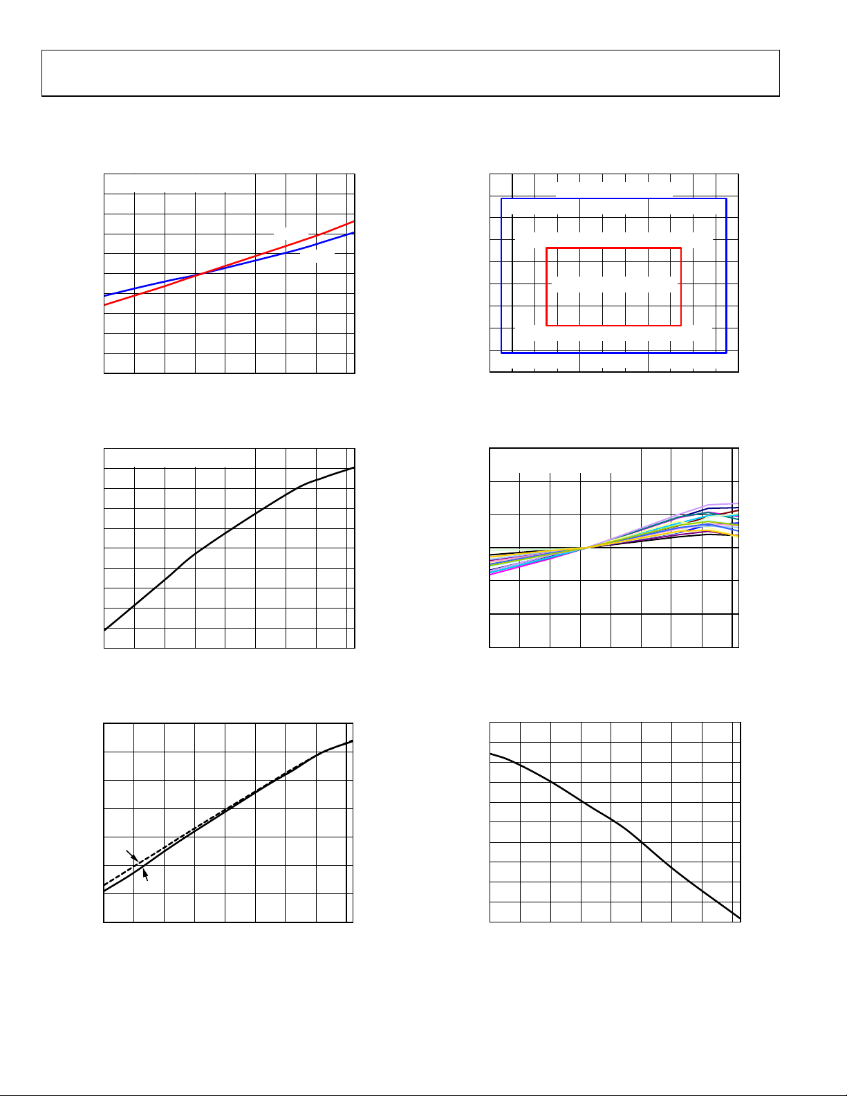
Figure 5. System Offset vs. Temperature
5
REPRESENTATIVE SAMPLES
4
3
2
1
0
–1
CMRR (µV/V)
–2
–3
–4
–5
–40 120100806040200–20
Figure 6. CMRR vs. Temperature (G = 0.8)
65
60
55
50
45
FALL
SLEW RATE (V/µs)
40
35
30
–40 120
RISE
Figure 7. Slew Rate vs. Temperature
TEMPERATURE (°C)
TEMPERATURE (°C)
TEMPERAT URE (°C)
= 1 kΩ, RTO, unless otherwise specified.
LOAD
G = 0.8
G = 0.4
09432-006
09432-005
100806040200–20
09432-015
10
8
6
4
2
0
–2
–4
COMMON-MODE VOLTAGE (V)
–6
–4.97V, –6. 25V
–8
–5.5 –4.5 –3.5 –2.5 –1.5 –0.5 0. 5 1.5 2. 5 3.5 4.5 5.5
VS = +5V, VOCM = +2.5V
VS = +3V, VOCM = +1.5V
–2.97V, –3.75V
OUTPUT VO LTAGE (V)
0V, +7.75V–4.97V, +7. 75V +4.95V, + 7.75V
0V, +3.25V–2.97V, +3 .25V
0V, –3.75V +2.95V, –3. 75V
0V, –6.25V
+2.95V, + 3.25V
+4.95V, –6. 25V
Figure 8. Input Common-Mode Voltage vs. Output Voltage,
= +5 V and +3 V
V
S
150
VIN = ±5V
REPRESENTATIVE SAMPLES
100
50
0
–50
GAIN ERRO R (µV/V)
–100
–150
–40 120100806040200–20
Figure 9. Gain Error vs. Temperature, V
TEMPERAT URE (°C)
= ±5 V
S
130
125
120
115
110
105
100
95
90
SHORT-CIRCUIT CURRENT (mA)
85
80
–40 120100806040200–20
TEMPERATURE (°C)
Figure 10. Short-Circuit Current vs. Temperature
09432-008
09432-100
09432-016
Rev. B | Page 8 of 24
 Loading...