Analog Devices AD847 Datasheet

High Speed, Low Power
a
FEATURES
Superior Performance
High Unity Gain BW: 50 MHz
Low Supply Current: 5.3 mA
High Slew Rate: 300 V/ms
Excellent Video Specifications
0.04% Differential Gain (NTSC and PAL)
0.198 Differential Phase (NTSC and PAL)
Drives Any Capacitive Load
Fast Settling Time to 0.1% (10 V Step): 65 ns
Excellent DC Performance
High Open-Loop Gain 5.5 V/mV (R
Low Input Offset Voltage: 0.5 mV
Specified for 65 V and 615 V Operation
Available in a Wide Variety of Options
Plastic DIP and SOIC Packages
Cerdip Package
Die Form
MIL-STD-883B Processing
Tape & Reel (EIA-481A Standard)
Dual Version Available: AD827 (8 Lead)
Enhanced Replacement for LM6361
Replacement for HA2544, HA2520/2/5 and EL2020
APPLICATIONS
Video Instrumentation
Imaging Equipment
Copiers, Fax, Scanners, Cameras
High Speed Cable Driver
High Speed DAC and Flash ADC Buffers
PRODUCT DESCRIPTION
The AD847 represents a breakthrough in high speed amplifiers
offering superior ac & dc performance and low power, all at low
cost. The excellent dc performance is demonstrated by its ±5 V
LOAD
= 1 kV)
Monolithic Op Amp
AD847
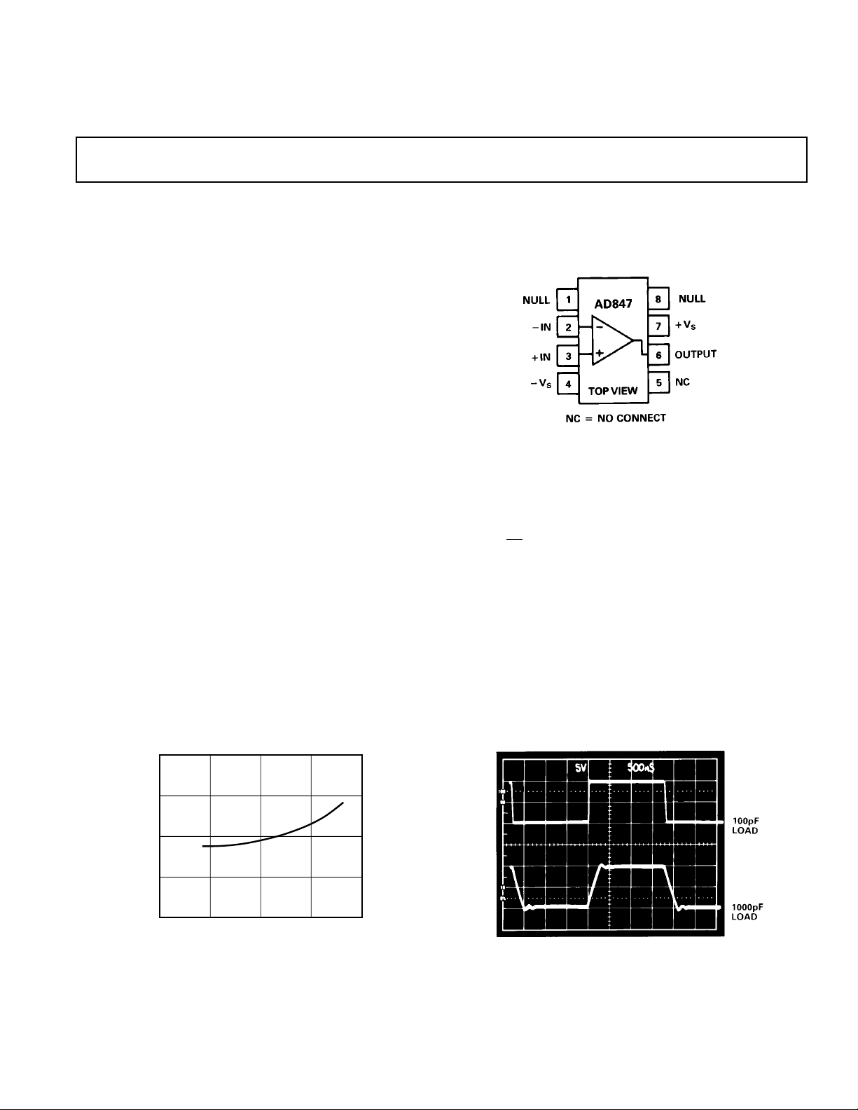
CONNECTION DIAGRAM
Plastic DIP (N),
Small Outline (R) and
Cerdip (Q) Packages
specifications which include an open-loop gain of 3500 V/V
(500 Ω load) and low input offset voltage of 0.5 mV. Commonmode rejection is a minimum of 78 dB. Output voltage swing is
±3 V into loads as low as 150 Ω. Analog Devices also offers
over 30 other high speed amplifiers from the low noise AD829
(1.7 nV/√
features 0.01% differential gain and 0.01° differential phase.
APPLICATION HIGHLIGHTS
1. As a buffer the AD847 offers a full-power bandwidth of
2. The low power and small outline package of the AD847
3. The AD847 is internally compensated for unity gain opera-
Hz) to the ultimate video amplifier, the AD811, which
12.7 MHz (5 V p-p with ±5 V supplies) making it outstanding as an input buffer for flash A/D converters.
make it very well suited for high density applications such as
multiple pole active filters.
tion and remains stable when driving any capacitive load.
6
5.5
5
4.5
QUIESCENT CURRENT – mA
4
020
Quiescent Current vs. Supply Voltage
REV. F
Information furnished by Analog Devices is believed to be accurate and
reliable. However, no responsibility is assumed by Analog Devices for its
use, nor for any infringements of patents or other rights of third parties
which may result from its use. No license is granted by implication or
otherwise under any patent or patent rights of Analog Devices.
5
SUPPLY VOLTAGE – ± Volts
10
15
AD847 Driving Capacitive Loads
One Technology Way, P.O. Box 9106, Norwood, MA 02062-9106, U.S.A.
Tel: 617/329-4700 Fax: 617/326-8703

AD847–SPECIFICA TIONS
(@ TA = +258C, unless otherwise noted)
Model AD847J AD847AR
INPUT OFFSET VOLTAGE
1
Conditions V
T
to T
MIN
MAX
S
±5 V 0.5 1 0.5 1 mV
Min Typ Max Min Typ Max Units
3.5 4 mV
Offset Drift 15 15 µV/°C
INPUT BIAS CURRENT ±5 V, ± 15 V 3.3 6.6 3.3 6.6 µA
T
MIN
to T
MAX
7.2 10 µA
INPUT OFFSET CURRENT ±5 V, ± 15 V 50 300 50 300 nA
T
to T
MIN
Offset Current Drift 0.3 0.3 nA/°C
OPEN-LOOP GAIN V
V
MAX
= ±2.5 V ±5 V
OUT
R
= 500 Ω 2 3.5 2 3.5 V/mV
LOAD
T
to T
MIN
R
LOAD
= ±10 V ±15 V
OUT
R
LOAD
T
MAX
= 150 Ω 1.6 1.6 V/mV
= 1 kΩ 3 5.5 3 5.5 V/mV
to T
MIN
MAX
1 1 V/mV
1.5 1.5 V/mV
400 500 nA
DYNAMIC PERFORMANCE
Unity Gain Bandwidth ±5 V 35 35 MHz
Full Power Bandwidth
Slew Rate
3
2
V
= 5 V p-p
OUT
R
= 500 Ω, ±5 V 12.7 12.7 MHz
LOAD
V
= 20 V p-p,
OUT
R
= 1 kΩ±15 V 4.7 4.7 MHz
LOAD
R
= 1 kΩ±5 V 200 200 V/µs
LOAD
±15 V 50 50 MHz
±15 V 225 300 225 300 V/µs
Settling Time
to 0.1%, R
to 0.01%, R
Phase Margin C
Differential Gain f ≈ 4.4 MHz, R
Differential Phase f ≈ 4.4 MHz, R
= 250 Ω –2.5 V to +2.5 V ±5 V 65 65 ns
LOAD
= 250 Ω –2.5 V to +2.5 V ±5 V 140 140 ns
LOAD
10 V Step, AV = –1 ±15 V 65 65 ns
10 V Step, AV = –1 ±15 V 120 120 ns
= 10 pF ± 15 V
LOAD
R
= 1 kΩ 50 50 Degree
LOAD
= 1 kΩ±15 V 0.04 0.04 %
LOAD
= 1 kΩ±15 V 0.19 0.19 Degree
LOAD
COMMON-MODE REJECTION VCM = ±2.5 V ±5 V 78 95 78 95 dB
VCM = ±12 V ±15 V 78 95 78 95 dB
T
MIN
to T
MAX
75 75 dB
POWER SUPPLY REJECTION VS = ±5 V to ± 15 V 75 86 75 86 dB
T
MIN
to T
MAX
72 72 dB
INPUT VOLTAGE NOISE f = 10 kHz ±15 V 15 15 nV/√Hz
INPUT CURRENT NOISE f = 10 kHz ±15 V 1.5 1.5 pA/√Hz
INPUT COMMON-MODE
VOLTAGE RANGE ± 5 V +4.3 +4.3 V
–3.4 –3.4 V
±15 V +14.3 +14.3 V
–13.4 –13.4 V
OUTPUT VOLTAGE SWING R
Short-Circuit Current ± 15 V 32 32 mA
= 500 Ω±5 V 3.0 3.6 3.0 3.6 ±V
LOAD
R
= 150 Ω±5 V 2.5 3 2.5 3 ± V
LOAD
R
= 1 kΩ±15 V 12 12 ±V
LOAD
R
= 500 Ω±15 V 10 10 ±V
LOAD
INPUT RESISTANCE 300 300 kΩ
INPUT CAPACITANCE 1.5 1.5 pF
OUTPUT RESISTANCE Open Loop 15 15 Ω
POWER SUPPLY
Operating Range 64.5 618 64.5 618 V
Quiescent Current ± 5 V 4.8 6.0 4.8 6.0 mA
T
to T
MIN
MAX
T
to T
MIN
MAX
N
OTES
l
Input Offset Voltage Specifications are guaranteed after 5 minutes at TA = +25°C.
2
Full Power Bandwidth = Slew Rate/2 π V
3
Slew Rate is measured on rising edge.
All min and max specifications are guaranteed. Specifications in boldface are 100% tested at final electrical test.
Specifications subject to change without notice.
PEAK
.
±15 V 5.3 6.3 5.3 6.3 mA
7.3 7.3 mA
7.6 7.6 mA
–2–
REV. F

AD847
Model AD847AQ AD847S
INPUT OFFSET VOLTAGE
Offset Drift 15 15 µV/°C
1
T
to T
MIN
MAX
Conditions V
S
±5 V 0.5 1 0.5 1 mV
Min Typ Max Min Typ Max Units
44mV
INPUT BIAS CURRENT ±5 V, ± 15 V 3.3 5 3.3 5 µA
T
MIN
to T
MAX
7.5 7.5 µA
INPUT OFFSET CURRENT ±5 V, ± 15 V 50 300 50 300 nA
T
MIN
to T
MAX
400 400 nA
Offset Current Drift 0.3 0.3 nA/°C
OPEN-LOOP GAIN V
= ±2.5 V ±5 V
OUT
R
= 500 Ω 2 3.5 2 3.5 V/mV
LOAD
T
to T
MIN
R
LOAD
V
= = ±10 V ±15 V
OUT
R
LOAD
T
MAX
= 150 Ω 1.6 1.6 V/mV
= 1 kΩ 3 5.5 3 5.5 V/mV
to T
MIN
MAX
11V/mV
1.5 1.5 V/mV
DYNAMIC PERFORMANCE
Unity Gain Bandwidth ±5 V 35 35 MHz
Full Power Bandwidth
Slew Rate
3
2
V
= 5 V p-p
OUT
R
= 500 Ω, ±5 V 12.7 12.7 MHz
LOAD
V
= 20 V p-p,
OUT
R
= 1 kΩ±15 V 4.7 4.7 MHz
LOAD
R
= 1 kΩ±5 V 200 200 V/µs
LOAD
±15 V 50 50 MHz
±15 V 225 300 225 300 V/µs
Settling Time
to 0.1%, R
= 250 Ω –2.5 V to +2.5 V ±5 V 65 65 ns
LOAD
10 V Step, AV = –1 ±15 V 65 65 ns
to 0.01%, R
= 250 Ω –2.5 V to +2.5 V ±5 V 140 140 ns
LOAD
10 V Step, AV = –1 ±15 V 120 120 ns
Phase Margin C
Differential Gain f ≈ 4.4 MHz, R
Differential Phase f ≈ 4.4 MHz, R
= 10 pF ± 15 V
LOAD
R
= 1 kΩ 50 50 Degree
LOAD
= 1 kΩ±15 V 0.04 0.04 %
LOAD
= 1 kΩ±15 V 0.19 0.19 Degree
LOAD
COMMON-MODE REJECTION VCM = ±2.5 V ±5 V 80 95 80 95 dB
VCM = ±12 V ±15 V 80 95 80 95 dB
T
MIN
to T
MAX
75 75 dB
POWER SUPPLY REJECTION VS = ±5 V to ±15 V 75 86 75 86 dB
T
MIN
to T
MAX
72 72 dB
INPUT VOLTAGE NOISE f = 10 kHz ±15 V 15 15 nV/√Hz
INPUT CURRENT NOISE f = 10 kHz ±15 V 1.5 1.5 pA/√Hz
INPUT COMMON-MODE
VOLTAGE RANGE ± 5 V +4.3 +4.3 V
–3.4 –3.4 V
±15 V +14.3 +14.3 V
–13.4 –13.4 V
OUTPUT VOLTAGE SWING R
Short-Circuit Current ± 15 V 32 32 mA
= 500 Ω±5 V 3.0 3.6 3.0 3.6 ±V
LOAD
R
= 150 Ω±5 V 2.5 3 2.5 3 ±V
LOAD
R
= 1 kΩ±15 V 12 12 ±V
LOAD
R
= 500 Ω±15 V 10 10 ±V
LOAD
INPUT RESISTANCE 300 300 kΩ
INPUT CAPACITANCE 1.5 1.5 pF
OUTPUT RESISTANCE Open Loop 15 15 Ω
POWER SUPPLY
Operating Range 64.5 618 64.5 618 V
Quiescent Current ± 5 V 4.8 5.7 4.8 5.7 mA
T
to T
MIN
MAX
T
to T
MIN
MAX
±15 V 5.3 6.3 5.3 6.3 mA
7.0 7.8 mA
7.6 8.4 mA
REV. F
–3–

AD847
ABSOLUTE MAXIMUM RATINGS
Supply Voltage . . . . . . . . . . . . . . . . . . . . . . . . . . . . . . . . ±18 V
Internal Power Dissipation
2
1
Plastic (N) . . . . . . . . . . . . . . . . . . . . . . . . . . . . . . 1.2 Watts
Small Outline (R) . . . . . . . . . . . . . . . . . . . . . . . . . 0.8 Watts
Cerdip (Q) . . . . . . . . . . . . . . . . . . . . . . . . . . . . . . 1.1 Watts
Input Voltage . . . . . . . . . . . . . . . . . . . . . . . . . . . . . . . . . . .±V
S
Differential Input Voltage . . . . . . . . . . . . . . . . . . . . . . . .±6 V
Storage Temperature Range (Q) . . . . . . . . . –65°C to +150°C
(N, R) . . . . . . . . . . . . . . . . . . . . . . . . . . . –65°C to +125°C
Junction Temperature . . . . . . . . . . . . . . . . . . . . . . . . . .175°C
Lead Temperature Range (Soldering 60 sec) . . . . . . . +300°C
NOTES
1
Stresses above those listed under “Absolute Maximum Ratings” may cause
permanent damage to the device. This is a stress rating only, and functional
operation of the device at these or any other conditions above those indicated in
the operational section of this specification is not implied. Exposure to absolute
maximum rating conditions for extended periods may affect device reliability.
2
Mini-DIP Package: θJA = 100°C/Watt; θJC = 33°C/Watt
Cerdip Package: θJA = 110°C/Watt; θJC = 30°C/Watt
Small Outline Package: θJA = 155°C/Watt; θJC = 33°C/Watt
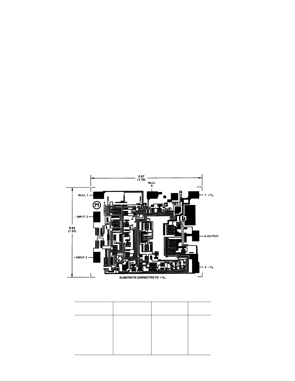
METALIZATION PHOTOGRAPH
Contact factory for latest dimensions.
Dimensions shown in inches and (mm).
ESD SUSCEPTIBILITY
ESD (electrostatic discharge) sensitive device. Electrostatic
charges as high as 4000 volts, which readily accumulate on the
human body and on test equipment, can discharge without detection. Although the AD847 features proprietary ESD protection circuitry, permanent damage may still occur on these
devices if they are subjected to high energy electrostatic discharges. Therefore, proper ESD precautions are recommended
to avoid any performance degradation or loss of functionality.
ORDERING GUIDE
Temperature Package Package
Models* Range – 8C Description Option
AD847JN 0 to +70 Plastic N-8
AD847JR 0 to +70 SOIC R-8
AD847AQ –40 to +85 Cerdip Q-8
AD847AR –40 to +85 SOIC R-8
AD847SQ –55 to +125 Cerdip Q-8
AD847SQ/883B –55 to +125 Cerdip Q-8
5962-8964701PA –55 to +125 Cerdip Q-8
*AD847 also available in J and S grade chips, and AD847JR and AD847AR are available
*in tape and reel.
–4–
REV. F
 Loading...