

8-Bit, 4-Channel Data
V
OUT
DGND
AG
DACAGADC
DATA I/O
(8 BITS)
M
U
X
T/H
8-BIT ADC
1.25 REF
8-BIT
DAC
RS
INT
BUSY
ST
DAC REG
ADC REG
CONTROL LOGIC
A0 A1
VDD (+5.0V)
RD WRCLK CS
AD8401
V
A
IN
V
B
IN
V
C
IN
V
D
IN
a
FEATURES
2 ms ADC with T/H
4-Channel MUX
AD899 Compatible
+5 Volt Operation
On-Chip Reference
4 ms Voltage Output DAC
Fast Bus Access Time—75 ns
APPLICATIONS
Servo Controls
Digitally Controlled Calibration
Process Control Equipment
GENERAL DESCRIPTION
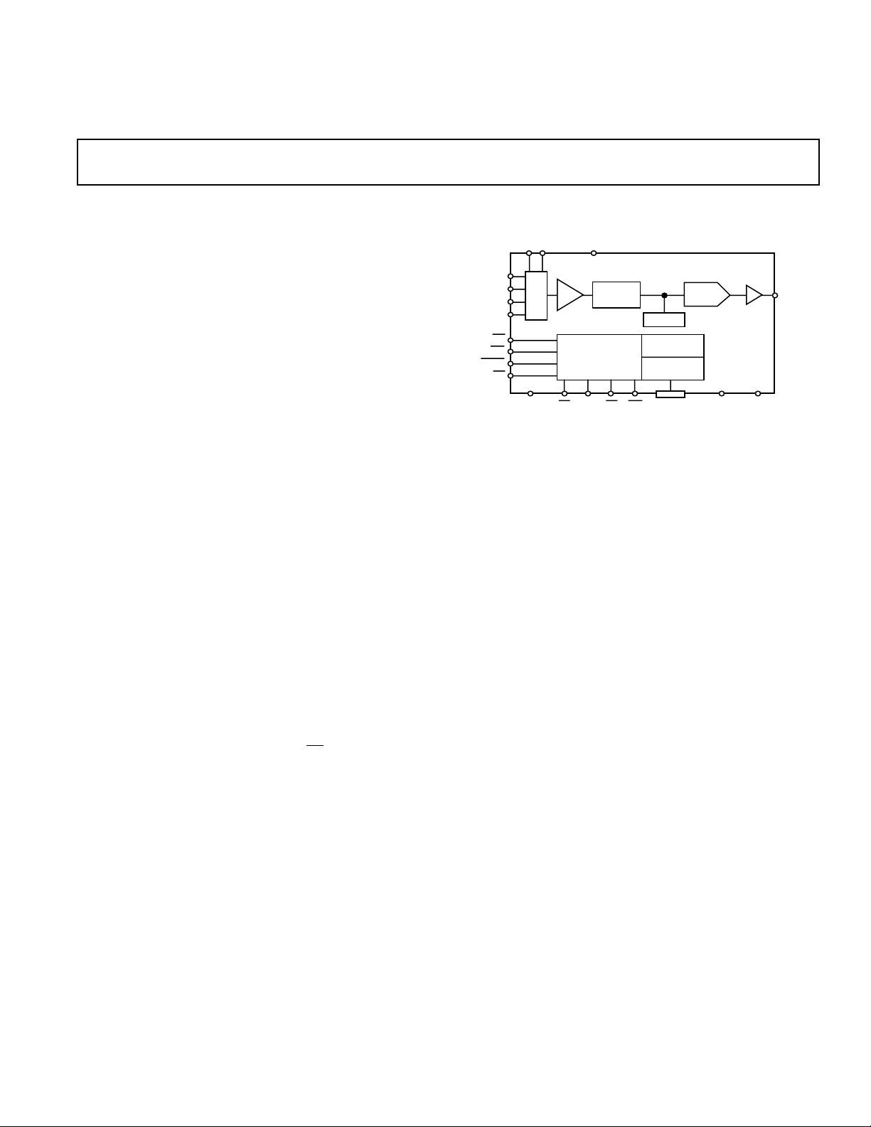
The AD8401 is a complete data acquisition and control system
containing ADC, DAC, 4-channel MUX, and internal voltage
reference. Built using CBCMOS, this monolithic circuit offers
the user a complete system with very high package density and
reliability.
The converter is a successive approximation ADC with T/H,
and is capable of operating with conversion times as short as
2 µs. Analog input bandwidth is 200 kHz, and DAC output volt-
age settling time is less than 4 µs, making the AD8401 capable
of controlling servo loops with speed and precision.
The 8-bit data interface provides both read and write operation
for parallel bus interfaces to microcontrollers and DSP processors. An external 5 MHz clock sets the 2 µs conversion rate.
Slower clocks reduce the conversion time and the internal power
dissipation. The standard control lines: Reset, Busy, Interrupt,
Read and Write complete the handshaking signals for microprocessor communication. A start trigger
cise sampling intervals in synchronous sampling applications.
ST input allows pre-
Acquisition System
AD8401
FUNCTIONAL BLOCK DIAGRAM
The input multiplexer addressing is designed for direct interface
to the AD899 hard-disk drive, read-channel device with no extra
hardware or special software. Analog input range levels are likewise compatible with the AD899.
The AD8401 is designed to operate from a single +5 volt supply, which will give an ADC input range of 0 V to 3.0 V, and
DAC output range of 0 V to 2.5 V.
The AD8401 is offered in the SOIC-28 surface mount package,
and is guaranteed to operate over the extended industrial temperature range of –40°C to +85°C.
REV. 0
Information furnished by Analog Devices is believed to be accurate and
reliable. However, no responsibility is assumed by Analog Devices for its
use, nor for any infringements of patents or other rights of third parties
which may result from its use. No license is granted by implication or
otherwise under any patent or patent rights of Analog Devices.
One Technology Way, P.O. Box 9106, Norwood, MA 02062-9106, U.S.A.
Tel: 617/329-4700 Fax: 617/326-8703

AD8401–SPECIFICA TIONS
ADC ELECTRICAL CHARACTERISTICS
(@ VDD = +5.0 V 6 5%, AG
unless otherwise noted)
DAC
= AG
= 0.0 V; f
ADC
= 5 MHz; –408C ≤ TA ≤ +858C,
CLK
Parameter Symbol Conditions Min Typ Max Units
STATIC PERFORMANCE
Resolution N 8 Bits
Total Unadjusted Error TUE ±3 LSB
Relative Accuracy INL –1 +1 LSB
Differential Nonlinearity DNL –1 +1 LSB
Offset Error V
Full-Scale Error A
∆Full-Scale/∆V
DD
OSE
E
TA = +25°C –4 +4 LSB
T
= Full Temp Range –6 +6 LSB
A
TA = +25°C –4 +4 LSB
T
= Full Temp Range –6 +6 LSB
A
TA = +25°C 1 LSB
DYNAMIC PERFORMANCE
Signal-to-Noise Ratio SNR 44 dB
Total Harmonic Distortion THD 48 dB
Intermodulation Distortion IMD 60 dB
Frequency Response 0 to 200 kHz 0.1 dB
Track/Hold Acquisition Time t
AQ
200 ns
ANALOG INPUTS (Applies to Inputs A, B. C, D)
Unipolar Input Range V
Input Current I
Input Capacitance C
IN
IN
IN
03V
–500 +500 µA
10 pF
LOGIC INPUTS
Clock Input Current Low I
Clock Input Current High I
Input Leakage Current I
CKL
CKH
L
LOGIC OUTPUTS (Applies to Outputs DB0–DB7,
Logic Output Low Voltage V
Logic Output High Voltage V
Output Leakage Current I
Output Capacitance C
CONVERSION TIME t
Specifications subject to change without notice.
OL
OH
OZ
OZ
C
VIN = 0 V 1.6 mA
VIN = V
DD
40 µA
CS, RD, RS, ST 10 µA
INT, BUSY)
IOL = 1.6 mA 0.4 V
IOH = 200 µA 4.0 V
CS = 1 (Except INT & BUSY)10µA
CS = 1 (Except INT & BUSY)10pF
External Clock 2 µs
Table I. Multiplexer Address Input Decode
A1 A0 Input Selected
00V
01V
10V
11V
A
IN
B
IN
C
IN
D
IN
–2–
REV. 0

AD8401
DAC ELECTRICAL CHARACTERISTICS
(@ VDD = +5.0 V 6 5%, AG
to AG
; –408C ≤ TA ≤ +858C, unless otherwise noted)
DAC
DAC
= AG
= 0.0 V; RL = 2 kV, CL = 100 pF
ADC
Parameter Symbol Conditions Min Typ Max Units
STATIC PERFORMANCE
Resolution N 8 Bits
Total Unadjusted Error TUE ±2 LSB
Relative Accuracy INL –1 +1 LSB
Differential Nonlinearity DNL –1 +1 LSB
Offset Error V
Full-Scale Error A
∆Full-Scale/∆V
DD
OSE
E
TA = +25°C –2 +2 LSB
T
= Full Temp Range –2.5 +2.5 LSB
A
TA = +25°C –3 +3 LSB
T
= Full Temp Range –4 +4 LSB
A
TA = +25°C –0.5 +0.5 LSB
Load Regulation at Full-Scale –0.2 +0.2 LSB
DYNAMIC PERFORMANCE
Signal-to-Noise Ratio SNR 44 dB
Total Harmonic Distortion THD 48 dB
ANALOG OUTPUT
Output Voltage Range OVR 0 +2.5 V
LOGIC INPUTS (Applies to DB0–DB7, CS, WR, RD, RS)
Logic Input Low Voltage V
Logic Input High Voltage V
Input Leakage Current I
Input Capacitance C
IL
IH
L
IL
2.4 V
–10 10 µA
0.8 V
10 pF
AC CHARACTERISTICS
Voltage Output Settling Time t
Positive Full-Scale Change t
Negative Full-Scale Change t
S
POS
NEG
To ±1/2 LSB of Final Value 2 4 µs
10% to 90% 1 2 µs
90% to 10% 2 4 µs
DAC Glitch Impulse 15 nV s
Digital Feedthrough 1 nV s
VIN to V
Isolation f = 50 kHz 60 dB
OUT
POWER REQUIREMENTS
Positive Supply Current I
Specifications subject to change without notice.
DD
No Load 13 mA
REV. 0
–3–
AD8401
DGND
10pF
3kΩ
DBN
DBN
10pF
3kΩ
+5V
DGND
TIMING ELECTRICAL SPECIFICATIONS
Parameters
1, 2, 3
(@ VDD = +5.0 V 6 5%, AG
unless otherwise noted)
Symbol Condition Min Typ Max Units
DAC
= AG
= 0.0 V; f
ADC
= 5 MHz; –408C ≤ TA ≤ +858C,
CLK
DAC TIMING (See Figure 8 Timing Diagram)
WR Pulse Width t
CS to WR Setup Time t
CS to WR Hold Time t
Data Setup Time t
Data Hold Time t
1
2
3
4
5
50 ns
0ns
0ns
60 ns
0ns
ADC TIMING (See Figures 6 and 7 Timing Diagrams)
ST Pulse Width t
ST to BUSY Delay t
BUSY to INT Delay t
BUSY to CS Delay t
CS to RD Setup Time t
RD Pulse Width
4
CS to RD Hold Time t
Data Access after
Data Access after
Bus Relinquish after
RD t
RD t
RD t
RD to INT Delay t
RD to BUSY Delay t
Data Valid after
BUSY t
Data Valid after BUSY t
NOTES
1
All input control signals are specified with tR = tF = 5 ns (10% to 90% of +5 V) and timed from a voltage level of 1.6 V.
2
t13 and t17 are measured with the load circuits of Figure 1 and defined as the time required for an output to cross either 0.8 V or 2.4 V.
3
t14 is defined as the time required for the data line to change 0.5 V when loaded with the circuit of Figure 2.
4
t15 is determined by t13.
DBN
3kΩ
CL
DGND
+5V
3kΩ
DBN
CL
DGND
6
7
8
9
10
t
11
12
13
13
14
15
16
17
17
CL = 20 pF 10 75 ns
CL = 100 pF 10 135 ns
CL = 20 pF 90 ns
CL = 100 pF 135 ns
40 ns
0ns
0ns
75 ns
0ns
10 70 ns
110 ns
30 ns
85 ns
110 ns
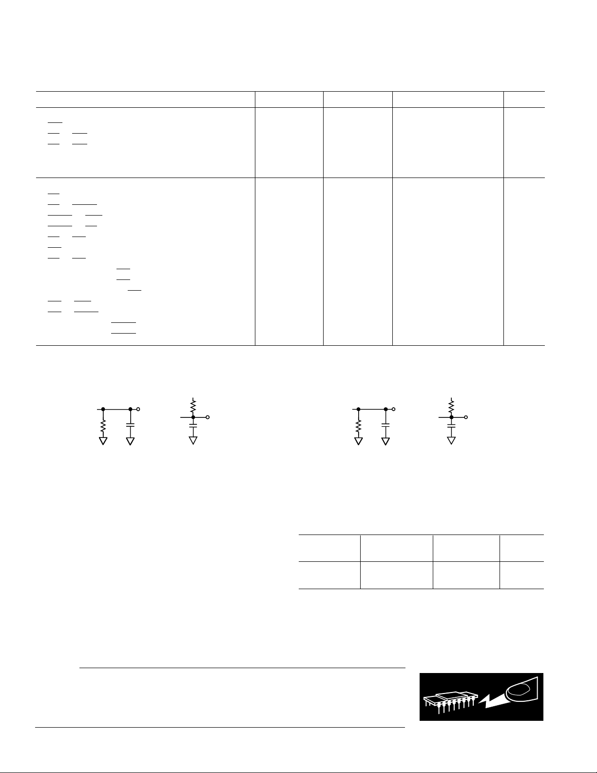
a. High Z to V
OH
b. High Z to V
OL
Figure 1. Load Circuits for Data Access Time Test
a. V
OH
Figure 2. Load Circuits for Bus Relinquish Time Test
ABSOLUTE MAXIMUM RATINGS*
Supply Voltage (VDD) . . . . . . . . . . . . . . . . . . . . . . . . . . . +8 V
Input Voltages . . . . . . . . . . . . . . . . . . . –0.3 V to V
+ 0.3 V
DD
Output Short-Circuit Duration . . . . . . . . . . . . . . . . Indefinite
Package Power Dissipation . . . . . . . . . . . . . . (T
Thermal Resistance θ
JA
28-Lead SOIC (R) . . . . . . . . . . . . . . . . . . . . . . . . . 53°C/W
Storage Temperature Range . . . . . . . . . . . . –65°C to +150°C
Operating Temperature Range . . . . . . . . . . . . –40°C to +85°C
Junction Temperature Range (T
max) . . . . –65°C to +150°C
J
Lead Temperature Range (Soldering, 60 sec) . . . . . . +300°C
*Stresses above those listed under “Absolute Maximum Ratings” may cause
permanent damage to the device. This is a stress rating only and functional
operation of the device at these or any other conditions above those indicated in the
operational sections of this specification is not implied. Exposure to absolute
maximum rating conditions for extended periods may affect device reliability.
max–TA)/θ
J
JA
Model* Range Description Option
AD8401AR –40°C to +85°C 28-Lead SOIC SOL-28
AD8401Chips +25°C Die
*The AD8401 contains 1257 transistors.
CAUTION
ESD (electrostatic discharge) sensitive device. Electrostatic charges as high as 4000 V readily
accumulate on the human body and test equipment and can discharge without detection.
Although the AD8401 features proprietary ESD protection circuitry, permanent damage may
occur on devices subjected to high energy electrostatic discharges. Therefore, proper ESD
–4–
precautions are recommended to avoid performance degradation or loss of functionality.
to High Z
b. VOL to High Z
ORDERING GUIDE
Temperature Package Package
WARNING!
ESD SENSITIVE DEVICE
REV. 0
 Loading...