a
500 MHz Four-Quadrant Multiplier
AD834
FEATURES
DC to >500 MHz Operation
Differential ⴞ1 V Full-Scale Inputs
Differential ⴞ4 mA Full-Scale Output Current
Low Distortion (≤0.05% for 0 dBm Input)
Supply Voltages from ⴞ4 V to ⴞ9 V
Low Power (280 mW typical at V
APPLICATIONS
High Speed Real Time Computation
Wideband Modulation and Gain Control
Signal Correlation and RF Power Measurement
Voltage Controlled Filters and Oscillators
Linear Keyers for High Resolution Television
Wideband True RMS
PRODUCT DESCRIPTION
The AD834 is a monolithic laser-trimmed four-quadrant analog
multiplier intended for use in high frequency applications, having a transconductance bandwidth (R
500 MHz from either of the differential voltage inputs. In multiplier modes, the typical total full-scale error is 0.5%, dependent
on the application mode and the external circuitry. Performance
is relatively insensitive to temperature and supply variations, due
to the use of stable biasing based on a bandgap reference generator and other design features.
To preserve the full bandwidth potential of the high speed
bipolar process used to fabricate the AD834, the outputs appear
as a differential pair of currents at open collectors. To provide a
single ended ground referenced voltage output, some form of external current to voltage conversion is needed. This may take the
form of a wideband transformer, balun, or active circuitry such
as an op amp. In some applications (such as power measurement) the subsequent signal processing may not need to have
high bandwidth.
The transfer function is accurately trimmed such that when
X = Y = ±1 V, the differential output is ±4 mA. This absolute
calibration allows the outputs of two or more AD834s to be
summed with precisely equal weighting, independent of the
accuracy of the load circuit.
The AD834J is specified for use over the commercial temperature range of 0°C to +70°C and is available in an 8-lead DIP
package and an 8-lead plastic SOIC package. AD834A is available in cerdip and 8-lead plastic SOIC packages for operation
over the industrial temperature range of –40°C to +85°C. The
AD834S/883B is specified for operation over the military temperature range of –55°C to +125°C and is available in the 8-lead
cerdip package. S-Grade chips are also available.
= ⴞ5 V)
S
= 50 Ω) in excess of
L
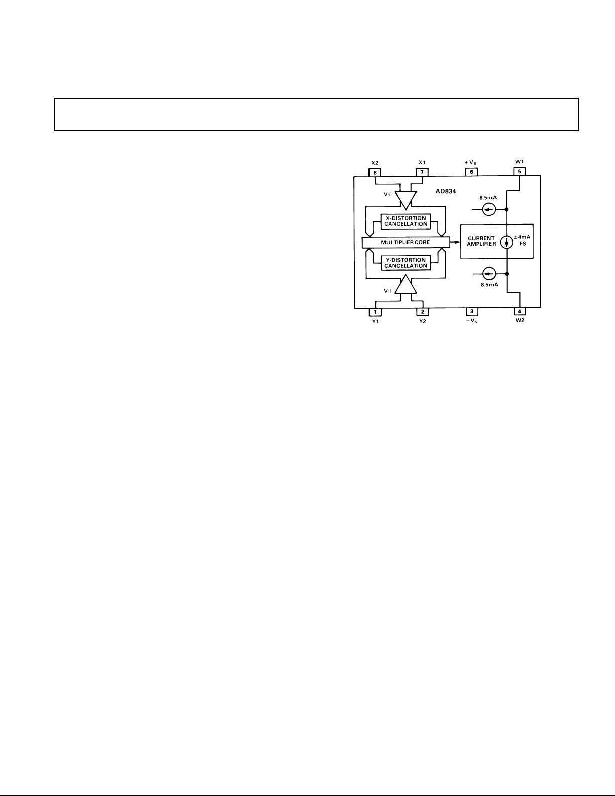
FUNCTIONAL BLOCK DIAGRAM
(W)
Two application notes featuring the AD834 (AN-212 and
AN-216) can now be obtained by calling 1-800-ANALOG-D.
For additional applications circuits consult the AD811 data sheet.
PRODUCT HIGHLIGHTS
l. The AD834 combines high static accuracy (low input and
output offsets and accurate scale factor) with very high bandwidth. As a four-quadrant multiplier or squarer, the response
extends from dc to an upper frequency limited mainly by
packaging and external board layout considerations. A large
signal bandwidth of over 500 MHz is attainable under optimum conditions.
2. The AD834 can be used in many high speed nonlinear
operations, such as square rooting, analog division, vector
addition and rms-to-dc conversion. In these modes, the
bandwidth is limited by the external active components.
3. Special design techniques result in low distortion levels (better
than –60 dB on either input) at high frequencies and low signal
feedthrough (typically –65 dB up to 20 MHz).
4. The AD834 exhibits low differential phase error over the input
range—typically 0.08° at 5 MHz and 0.8° at 50 MHz. The
large signal transient response is free from overshoot, and has
an intrinsic rise time of 500 ps, typically settling to within 1%
in under 5 ns.
5. The nonloading, high impedance, differential inputs simplify
the application of the AD834.
REV. C
Information furnished by Analog Devices is believed to be accurate and
reliable. However, no responsibility is assumed by Analog Devices for its
use, nor for any infringements of patents or other rights of third parties
which may result from its use. No license is granted by implication or
otherwise under any patent or patent rights of Analog Devices.
One Technology Way, P.O. Box 9106, Norwood, MA 02062-9106, U.S.A.
Tel: 781/329-4700 World Wide Web Site: http://www.analog.com
Fax: 781/326-8703 © Analog Devices, Inc., 2000

AD834–SPECIFICATIONS
(TA = +25ⴗC and ⴞVS = ⴞ5 V, unless otherwise noted; dBm assumes 50 ⍀ load.)
Model Conditions Min Typ Max Min Typ Max Units
AD834J AD834A, S
MULTIPLIER PERFORMANCE
XY
Transfer Function
Total Error1 (Figure 6) –1 V ≤ X, Y < +1 V ±0.5 ⴞ2 ±0.5 ⴞ2 % FS
vs. Temperature T
vs. Supplies
Linearity
Bandwidth
2
3
4
to T
MIN
MAX
±4 V to ±6 V 0.1 0.3 0.1 0.3 % FS/V
See Figure 5 500 500 MHz
W =
±0.5 ⴞ1 ± 0.5 ⴞ1 % FS
(1V )
× 4 mA
2
XY
W =
(1V )
× 4 mA
2
±1.5 ⴞ3 % FS
Feedthrough, X X = ±1 V, Y = Nulled 0.2 0.3 0.2 0.3 % FS
Feedthrough, Y X = Nulled, Y = ± 1 V 0.1 0.2 0.1 0.2 % FS
AC Feedthrough, X
5
X = 0 dBm, Y = Nulled
f = 10 MHz –65 –65 dB
AC Feedthrough, Y
5
f = 100 MHz –50 –50 dB
X = Nulled, Y = 0 dBm
f = 10 MHz –70 –70 dB
f = 100 MHz –50 –50 dB
INPUTS (X1, X2, Y1, Y2)
Full-Scale Range Differential ±1 ±1V
Clipping Level Differential ⴞ1.1 ±1.3 ⴞ1.1 ±1.3 V
Input Resistance Differential 25 25 kΩ
Offset Voltage 0.5 3 0.5 3 mV
vs. Temperature T
vs. Supplies
2
MIN
to T
MAX
10 10 µV/°C
44mV
±4 V to ±6 V 100 300 100 300 µV/V
Bias Current 45 45 µA
Common-Mode Rejection f ≤ 100 kHz; 1 V p-p 70 70 dB
Nonlinearity, X Y = 1 V; X = ±1 V 0.2 0.5 0.2 0.5 % FS
Nonlinearity, Y X = 1 V; Y = ± 1 V 0.1 0.3 0.1 0.3 % FS
Distortion, X X = 0 dBm, Y = 1 V
f = 10 MHz –60 –60 dB
f = 100 MHz –44 –44 dB
Distortion, Y X = 1 V, Y = 0 dBm
f = 10 MHz –65 –65 dB
f = 100 MHz –50 –50 dB
OUTPUTS (W1, W2)
Zero Signal Current Each Output 8.5 8.5 mA
Differential Offset X = 0, Y = 0 ±20 ⴞ60 ±20 ⴞ60 µA
vs. Temperature T
MIN
to T
MAX
40 40 nA/°C
ⴞ60 µA
Scaling Current Differential 3.96 4 4.04 3.96 4 4.04 mA
Output Compliance 4.75 9 4.75 9 V
Noise Spectral Density f = 10 Hz to 1 MHz 16 16 nV/√Hz
Outputs into 50 Ω Load
POWER SUPPLIES
Operating Range ±4 ±9 ±4 ±9V
Quiescent Current
+V
S
–V
S
6
T
to T
MIN
MAX
11 14 11 14 mA
28 35 28 35 mA
TEMPERATURE RANGE
Operating, Rated Performance
Commercial (0°C to +70°C) AD834J
Military (–55°C to +125°C) AD834S
Industrial (–40°C to +85°C) AD834A
PACKAGE OPTIONS
8-Pin SOIC (R) AD834JR, REEL, REEL7 AD834AR
8-Pin Cerdip (Q) AD834AQ, SQ/883B
8-Pin Plastic DIP (N) AD834JN
NOTES
1
Error is defined as the maximum deviation from the ideal output, and expressed as a percentage of the full-scale output.
2
Both supplies taken simultaneously; sinusoidal input at f ≤ 10 kHz.
3
Linearity is defined as residual error after compensating for input offset voltage, output offset current and scaling current errors.
4
Bandwidth is guaranteed when configured in squarer mode. See Figure 5.
5
Sine input; relative to full-scale output; zero input port nulled; represents feedthrough of the fundamental.
6
Negative supply current is equal to the sum of positive supply current, the signal currents into each output, W1 and W2, and the input bias currents.
Specifications in boldface are tested on all production units at final electrical test. Results from those tests are used to calculate outgoing quality levels.
Specifications subject to c
hange without notice.
–2–
REV. C

AD834
ABSOLUTE MAXIMUM RATINGS*
Supply Voltage (+VS to –VS) . . . . . . . . . . . . . . . . . . . . . . 18 V
Internal Power Dissipation . . . . . . . . . . . . . . . . . . . . 500 mW
Input Voltages (X1, X2, Y1, Y2) . . . . . . . . . . . . . . . . . . . .+V
S
Operating Temperature Range
AD834J . . . . . . . . . . . . . . . . . . . . . . . . . . . . . 0°C to +70°C
AD834A . . . . . . . . . . . . . . . . . . . . . . . . . . . –40°C to +85°C
AD834S/883B . . . . . . . . . . . . . . . . . . . . . –55°C to +125°C
Storage Temperature Range (Q) . . . . . . . . . –65°C to +150°C
Storage Temperature Range (R, N) . . . . . . . –65°C to +125°C
Lead Temperature (Soldering 60 sec) . . . . . . . . . . . . .+300°C
ESD Rating . . . . . . . . . . . . . . . . . . . . . . . . . . . . . . . . . . 500 V
*Stresses above those listed under Absolute Maximum Ratings may cause perma-
nent damage to the devices. This is a stress rating only; functional operation of the
device at these or any other conditions above those indicated in the operational
section of this specification is not implied. Exposure to absolute maximum rating
conditions for extended periods may affect device reliability.
THERMAL CHARACTERISTICS
JC
JA
8-Pin Cerdip Package (Q) 30°C/W 110°C/W
8-Pin Plastic SOIC (R) 45°C/W 165°C/W
8-Pin Plastic Mini-DIP (N) 50°C/W 99°C/W
ORDERING GUIDE
Temperature Package
Model Range Option*
AD834JN 0°C to +70°C N-8
AD834JR 0°C to +70°C SO-8
AD834JR-REEL 0°C to +70°C SO-8
AD834JR-REEL7 0°C to +70°C SO-8
AD834AR –40°C to +85°C SO-8
AD834AQ –40°C to +85°C Q-8
AD834SQ/883B –55°C to +125°C Q-8
AD834S CHIPS –55°C to +125°C DIE
*N = Plastic DIP; Q = Cerdip; SO = Small Outline IC (SOIC) Package.
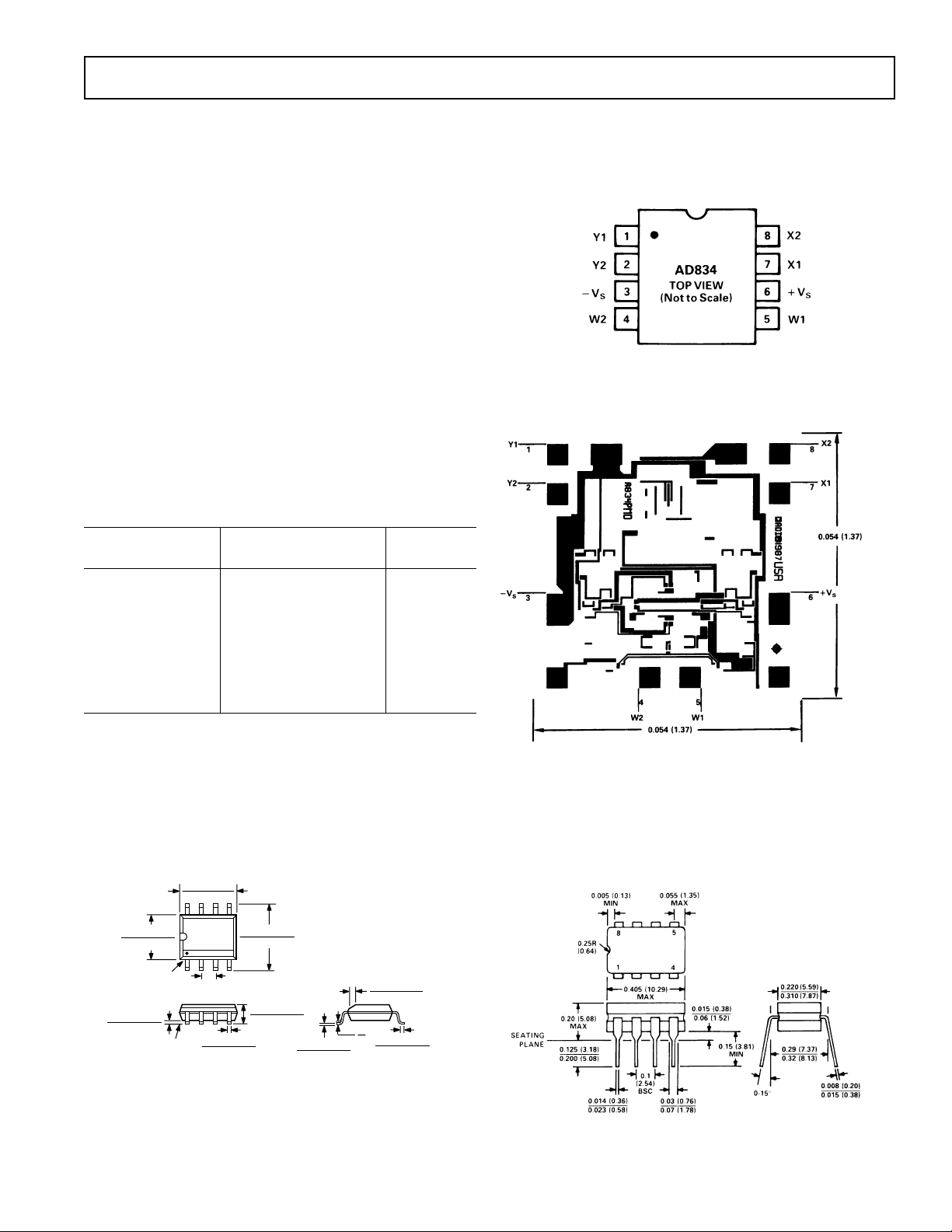
CONNECTION DIAGRAM
Small Outline (R) Package
Plastic DIP (N) Package
Cerdip (Q) Package
METALIZATION PHOTOGRAPH
CHIP DIMENSIONS AND BONDING DIAGRAM
Dimensions shown in inches and (mm).
Contact factory for latest dimensions.
0.0098 (0.25)
0.0040 (0.10)
REV. C
0.1574 (4.00)
0.1497 (3.80)
PIN 1
SEATING
PLANE
Small Outline (SO-8) Package
0.1968 (5.00)
0.1890 (4.80)
85
0.0500 (1.27)
0.2440 (6.20)
0.2284 (5.80)
41
BSC
0.0192 (0.49)
0.0138 (0.35)
0.0688 (1.75)
0.0532 (1.35)
0.0098 (0.25)
0.0075 (0.19)
0.0196 (0.50)
0.0099 (0.25)
8ⴗ
0.0500 (1.27)
0ⴗ
0.0160 (0.41)
OUTLINE DIMENSIONS
Dimensions shown in inches and (mm).
Cerdip (Q) Package
ⴛ 45ⴗ
–3–
 Loading...