Ultralow Noise VGAs with
VINV
V
Preamplifier and Programmable R
FEATURES
Ultralow noise preamplifier
Voltage noise = 0.74 nV/√Hz
Current noise = 2.5 pA/√Hz
3 dB bandwidth
AD8331: 120 MHz
AD8332, AD8334: 100 MHz
Low power
AD8331: 125 mW/channel
AD8332, AD8334: 145 mW/channel
Wide gain range with programmable postamp
−4.5 dB to +43.5 dB
+7.5 dB to +55.5 dB
Low output-referred noise: 48 nV/√Hz typical
Active input impedance matching
Optimized for 10-bit/12-bit ADCs
Selectable output clamping level
Single 5 V supply operation
AD8332 and AD8334 available in lead frame chip scale package
APPLICATIONS
Ultrasound and sonar time-gain controls
High performance AGC systems
I/Q signal processing
High speed, dual ADC drivers
GENERAL DESCRIPTION
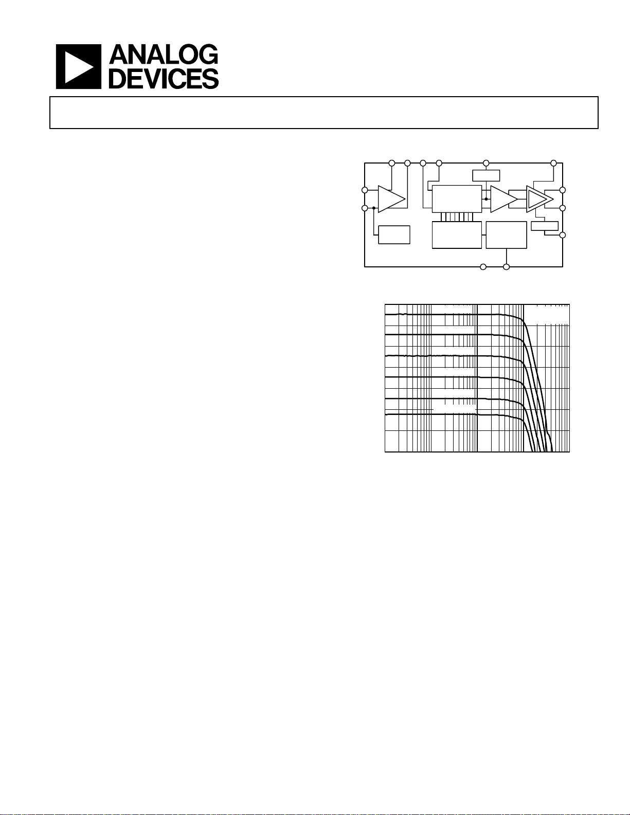
The AD8331/AD8332/AD8334 are single-, dual-, and quadchannel ultralow noise, linear-in-dB, variable gain amplifiers
(VGAs). Optimized for ultrasound systems, they are usable as a
low noise variable gain element at frequencies up to 120 MHz.
Included in each channel are an ultralow noise preamplifier
(LNA), an X-AMP® VGA with 48 dB of gain range, and a
selectable gain postamplifier with adjustable output limiting.
The LNA gain is 19 dB with a single-ended input and
differential outputs. Using a single resistor, the LNA input
impedance can be adjusted to match a signal source without
compromising noise performance.
The 48 dB gain range of the VGA makes these devices suitable
for a variety of applications. Excellent bandwidth uniformity is
maintained across the entire range. The gain control interface
provides precise linear-in-dB scaling of 50 dB/V for control
voltages between 40 mV and 1 V. Factory trim ensures excellent
part-to-part and channel-to-channel gain matching.
Rev. E
Information furnished by Analog Devices is believed to be accurate and reliable. However, no
responsibility is assumed by Anal og Devices for its use, nor for any infringements of patents or ot her
rights of third parties that may result from its use. Specifications subject to change without notice. No
license is granted by implication or otherwise under any patent or patent rights of Analog Devices.
Trademarks and registered trademarks are the property of their respective owners.
AD8331/AD8332/AD8334
FUNCTIONAL BLOCK DIAGRAM
IPLOPLON
LNA
INH
LMD
+
19dB
–
LNA VCM
BIAS
AD8331/AD8332/AD8334
–
48dB
ATTENUATOR
+
VGA BIAS AND
INTERPOL ATOR
Figure 1. Signal Path Block Diagram
60
50
40
30
20
GAIN (dB)
10
0
–10
100k 1M 10M 100M 1G
V
GAIN
V
GAIN
V
GAIN
V
GAIN
V
GAIN
V
GAIN
FREQUENCY (Hz)
Figure 2. Frequency Response vs. Gain
Differential signal paths result in superb second- and thirdorder distortion performance and low crosstalk.
The VGA’s low output-referred noise is advantageous in driving
high speed differential ADCs. The gain of the postamplifier can
be pin selected to 3.5 dB or 15.5 dB to optimize gain range and
output noise for 12-bit or 10-bit converter applications. The
output can be limited to a user-selected clamping level,
preventing input overload to a subsequent ADC. An external
resistor adjusts the clamping level.
The operating temperature range is −40°C to +85°C. The
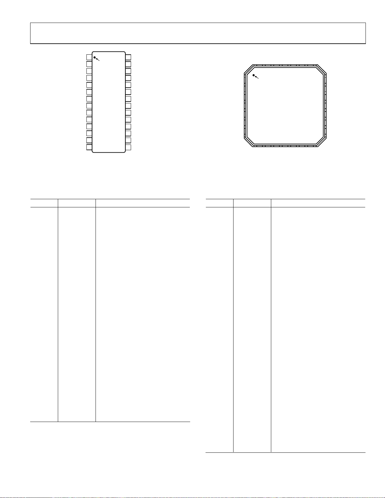
AD8331 is available in a 20-lead QSOP package, the AD8332 is
available in 28-lead TSSOP and 32-lead LFCSP packages, and
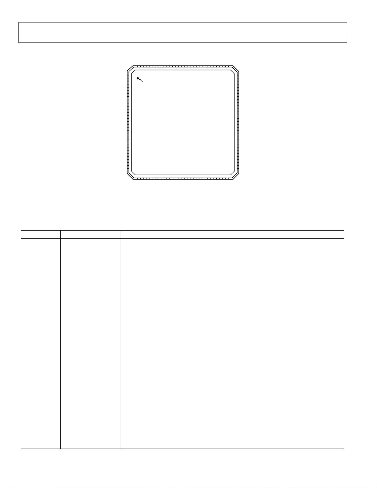
the AD8334 is available in a 64-lead LFCSP package.
One Technology Way, P.O. Box 9106, Norwood, MA 02062-9106, U.S.A.
Tel: 781.329.4700 www.analog.com
Fax: 781.461.3113 ©2006 Analog Devices, Inc. All rights reserved.
= 1V
= 0.8V
= 0.6V
= 0.4V
= 0.2V
= 0V
V
ENB
CM
MID
3.5dB/15. 5dB
21dB
GAIN
CONTROL
INTERFACE
GAIN
PA
CLAMP
HIGH GAIN
MODE
HILO
VOH
VOL
RCLMP
03199-002
IN
03199-001

AD8331/AD8332/AD8334
TABLE OF CONTENTS
Features .............................................................................................. 1
Variable Gain Amplifier ............................................................ 27
Applications....................................................................................... 1
General Description......................................................................... 1
Functional Block Diagram .............................................................. 1
Revision History ............................................................................... 3
Specifications..................................................................................... 4
Absolute Maximum Ratings............................................................ 7
ESD Caution.................................................................................. 7
Pin Configurations and Function Descriptions ...........................8
Typical Performance Characteristics........................................... 12
Test Circ uit s .....................................................................................20
Measurement Considerations................................................... 20
Theory of Operation ...................................................................... 24
Overview...................................................................................... 24
Low Noise Amplifier (LNA)..................................................... 25
Postamplifier............................................................................... 28
Applications..................................................................................... 30
LNA—External Components.................................................... 30
Driving ADCs............................................................................. 32
Overload...................................................................................... 32
Optional Input Overload Protection. ...................................... 33
Layout, Grounding, and Bypassing.......................................... 33
Multiple Input Matching ........................................................... 33
Disabling the LNA...................................................................... 33
Ultrasound TGC Application................................................... 34
High Density Quad Layout ....................................................... 34
Outline Dimensions .......................................................................39
Ordering Guide .......................................................................... 40
Rev. E | Page 2 of 40

AD8331/AD8332/AD8334
REVISION HISTORY
4/06—Rev. D to Rev. E
Added AD8334................................................................... Universal
Changes to Figure 1 and Figure 2....................................................1
Changes to Table 1 ............................................................................4
Changes to Table 2 ............................................................................7
Changes to Figure 7 through Figure 9 and Figure 12.................12
Changes to Figure 13, Figure 14, Figure 16, and Figure 18.......13
Changes to Figure 23 and Figure 24 .............................................14
Changes to Figure 25 through Figure 27......................................15
Changes to Figure 31 and Figure 33 through Figure 36.............16
Changes to Figure 37 through Figure 42......................................17
Changes to Figure 43, Figure 44, and Figure 48..........................18
Changes to Figure 49, Figure 50, and Figure 54..........................19
Inserted Figure 56 and Figure 57 ..................................................20
Inserted Figure 58, Figure 59, and Figure 61...............................21
Changes to Figure 60 ......................................................................21
Inserted Figure 63 and Figure 65 ..................................................22
Changes to Figure 64 ......................................................................22
Moved Measurement Considerations Section ............................2
Inserted Figure 67 and Figure 68 ..................................................23
Inserted Figure 70 and Figure 71 ..................................................24
Change to Figure 72........................................................................24
Changes to Figure 73 and Low Noise Amplifier Section ...........25
Changes to Postamplifier Section .................................................28
Changes to Figure 80 ......................................................................29
Changes to LNA—External Components Section......................30
Changes to Logic Inputs—ENB, MODE, and HILO Section....31
Changes to Output Decoupling and Overload Sections ............32
Changes to Layout, Grounding, and Bypassing Section............33
Changes to Ultrasound TGC Application Section......................34
Added High Density Quad Layout Section .................................34
Inserted Figure 94............................................................................38
Updated Outline Dimensions........................................................39
Changes to Ordering Guide...........................................................40
3/06—Rev. C to Rev. D
Updated Format .................................................................Universal
Changes to Features and General Description..............................1
Changes to Table 1 ............................................................................3
Changes to Table 2 ............................................................................6
Changes to Ordering Guide...........................................................34
11/03—Rev. B to Rev. C
Addition of New Part......................................................... Universal
Changes to Figures............................................................. Universal
Updated Outline Dimensions........................................................32
5/03—Rev. A to Rev. B
Edits to Ordering Guide.................................................................32
Edits to Ultrasound TGC Application Section ...........................25
Added Figure 71, Figure 72, and Figure 73..................................26
Updated Outline Dimensions........................................................31
2/03—Rev. 0 to Rev. A
0
Edits to Ordering Guide.................................................................32
Rev. E | Page 3 of 40

AD8331/AD8332/AD8334
SPECIFICATIONS
TA = 25°C, VS = 5 V, RL = 500 Ω, RS = RIN = 50 Ω, RFB = 280 Ω, CSH = 22 pF, f = 10 MHz, R
−4.5 dB to +43.5 dB gain (HILO = LO), and differential output voltage, unless otherwise specified.
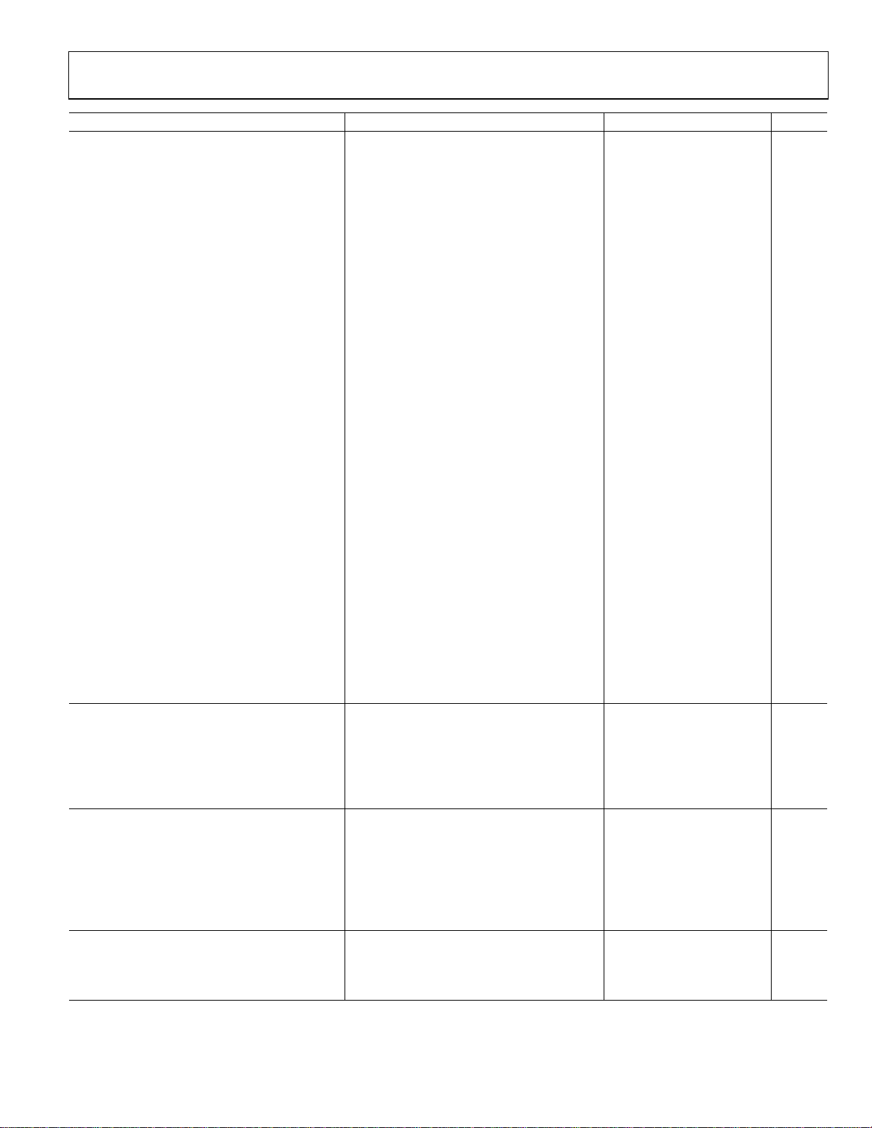
Table 1.
Parameter Conditions Min Typ Max Unit
LNA CHARACTERISTICS
Gain Single-ended input to differential output 19 dB
Input to output (single ended) 13 dB
Input Voltage Range AC-coupled ±275 mV
Input Resistance RFB = 280 Ω 50 Ω
R
R
R
R
= 412 Ω 75 Ω
FB
= 562 Ω 100 Ω
FB
= 1.13 kΩ 200 Ω
FB
= ∞ 6 kΩ
FB
Input Capacitance 13 pF
Output Impedance Single-ended, either output 5 Ω
−3 dB Small Signal Bandwidth V
= 0.2 V p-p 130 MHz
OUT
Slew Rate 650 V/μs
Input Voltage Noise RS = 0 Ω, HI or LO gain, RFB = ∞, f = 5 MHz 0.74 nV/√Hz
Input Current Noise RFB = ∞, HI or LO gain, f = 5 MHz 2.5 pA/√Hz
Noise Figure f = 10 MHz, LOP output
Active Termination Match RS = RIN = 50 Ω 3.7 dB
Unterminated RS = 50 Ω, RFB = ∞ 2.5 dB
Harmonic Distortion @ LOP1 or LOP2 V
= 0.5 V p-p, single-ended, f = 10 MHz
OUT
HD2 −56 dBc
HD3 −70 dBc
Output Short-Circuit Current Pin LON, Pin LOP 165 mA
LNA + VGA CHARACTERISTICS
−3 dB Small Signal Bandwidth V
= 0.2 V p-p
OUT
AD8331 120 MHz
AD8332, AD8334 100 MHz
−3 dB Large Signal Bandwidth V
= 2 V p-p
OUT
AD8331 110 MHz
AD8332, AD8334 90 MHz
Slew Rate
AD8331 LO gain 300 V/μs
HI gain 1200 V/μs
AD8332, AD8334 LO gain 275 V/μs
HI gain 1100 V/μs
Input Voltage Noise RS = 0 Ω, HI or LO gain, RFB = ∞, f = 5 MHz 0.82 nV/√Hz
Noise Figure V
= 1.0 V
GAIN
Active Termination Match RS = RIN = 50 Ω, f = 10 MHz, measured 4.15 dB
R
= RIN = 200 Ω, f = 5 MHz, simulated 2.0 dB
S
Unterminated RS = 50 Ω, RFB = ∞, f = 10 MHz, measured 2.5 dB
R
= 200 Ω, RFB = ∞, f = 5 MHz, simulated 1.0 dB
S
Output-Referred Noise
AD8331 V
V
AD8332, AD8334 V
V
= 0.5 V, LO gain 48 nV/√Hz
GAIN
= 0.5 V, HI gain 178 nV/√Hz
GAIN
= 0.5 V, LO gain 40 nV/√Hz
GAIN
= 0.5 V, HI gain 150 nV/√Hz
GAIN
Output Impedance, Postamplifier DC to 1 MHz 1 Ω
= ∞, CL = 1 pF, VCM pin floating,
CLMP
Rev. E | Page 4 of 40
AD8331/AD8332/AD8334
Parameter Conditions Min Typ Max Unit
Output Signal Range, Postamplifier RL ≥ 500 Ω, unclamped, either pin VCM ± 1.125 V
Differential 4.5 V p-p
Output Offset Voltage V
AD8331 Differential −50 ±5 +50 mV
Common mode −125 −25 +100 mV
AD8332, AD8334 Differential −20 ±5 +20 mV
Common mode −125 –25 +100 mV
Output Short-Circuit Current 45 mA
Harmonic Distortion V
AD8331
HD2 f = 1 MHz −88 dBc
HD3 −85 dBc
HD2 f = 10 MHz −68 dBc
HD3 −65 dBc
AD8332, AD8334
HD2 f = 1 MHz −82 dBc
HD3 −85 dBc
HD2 f = 10 MHz −62 dBc
HD3 −66 dBc
Input 1 dB Compression Point V
Two-Tone Intermodulation Distortion (IMD3)
AD8331 V
V
AD8332, AD8334 V
V
Output Third-Order Intercept
AD8331 V
V
AD8332, AD8334 V
V
Channel-to-Channel Crosstalk (AD8332, AD8334) V
Overload Recovery V
Group Delay Variation 5 MHz < f < 50 MHz, full gain range ±2 ns
ACCURACY
Absolute Gain Error
2
0.10 V < V
0.95 V < V
Gain Law Conformance
3
Channel-to-Channel Gain Matching 0.1 V < V
GAIN CONTROL INTERFACE (Pin GAIN)
Gain Scaling Factor 0.10 V < V
Gain Range LO gain −4.5 to +43.5 dB
HI gain 7.5 to 55.5 dB
Input Voltage (V
) Range 0 to 1.0 V
GAIN
Input Impedance 10 MΩ
Response Time 48 dB gain change to 90% full scale 500 ns
COMMON-MODE INTERFACE (PIN VCMn)
Input Resistance
4
Output CM Offset Voltage VCM = 2.5 V −125 −25 +100 mV
Voltage Range V
= 0.5 V
GAIN
= 0.5 V, V
GAIN
= 0.25 V, V
GAIN
= 0.72 V, V
GAIN
= 0.5 V, V
GAIN
= 0.72 V, V
GAIN
= 0.5 V, V
GAIN
= 0.5 V, V
GAIN
= 0.5 V, V
GAIN
= 0.5 V, V
GAIN
= 0.5 V, V
GAIN
= 0.5 V, V
GAIN
= 1.0 V, VIN = 50 mV p-p/1 V p-p, f = 10 MHz 5 ns
GAIN
0.05 V < V
0.1 V < V
GAIN
GAIN
= 1 V p-p, HI gain
OUT
= 1 V p-p, f = 1 MHz to 10 MHz 1 dBm
OUT
= 1 V p-p, f = 1 MHz −80 dBc
OUT
= 1 V p-p, f = 10 MHz −72 dBc
OUT
= 1 V p-p, f = 1 MHz −78 dBc
OUT
= 1 V p-p, f = 10 MHz −74 dBc
OUT
= 1 V p-p, f = 1 MHz 38 dBm
OUT
= 1 V p-p, f = 10 MHz 33 dBm
OUT
= 1 V p-p, f = 1 MHz 35 dBm
OUT
= 1 V p-p, f = 10 MHz 32 dBm
OUT
= 1 V p-p, f = 1 MHz −98 dB
OUT
< 0.10 V −1 +0.5 +2 dB
GAIN
< 0.95 V −1 ±0.3 +1 dB
GAIN
< 1.0 V −2 −1 +1 dB
GAIN
< 0.95 V ±0.2 dB
< 0.95 V ±0.1 dB
< 0.95 V 48.5 50 51.5 dB/V
GAIN
1
Current limited to ±1 mA 30 Ω
= 2.0 V p-p 1.5 to 3.5 V
OUT
Rev. E | Page 5 of 40

AD8331/AD8332/AD8334
Parameter Conditions Min Typ Max Unit
ENABLE INTERFACE
(PIN ENB, PIN ENBL, PIN ENBV)
Logic Level to Enable Power 2.25 5 V
Logic Level to Disable Power 0 1.0 V
Input Resistance Pin ENB 25 kΩ
Pin ENBL 40 kΩ
Pin ENBV 70 kΩ
Power-Up Response Time V
V
HILO GAIN RANGE INTERFACE (PIN HILO)
Logic Level to Select HI Gain Range 2.25 5 V
Logic Level to Select LO Gain Range 0 1.0 V
Input Resistance 50 kΩ
OUTPUT CLAMP INTERFACE
(PIN RCLMP; HI OR LO GAIN)
Accuracy
HILO = LO R
HILO = HI R
MODE INTERFACE (PIN MODE)
Logic Level for Positive Gain Slope 0 1.0 V
Logic Level for Negative Gain Slope 2.25 5 V
Input Resistance 200 kΩ
POWER SUPPLY (PIN VPS1, PIN VPS2,
PIN VPSV, PIN VPSL, PIN VPOS)
Supply Voltage 4.5 5.0 5.5 V
Quiescent Current per Channel
AD8331 20 25 mA
AD8332, AD8334 20 29 mA
Power Dissipation per channel No signal
AD8331 125 mW
AD8332, AD8334 145 mW
Power-Down Current
AD8332 (VGA and LNA Disabled) 50 300 600 μA
AD8331 (VGA and LNA Disabled) 50 240 400 μA
LNA Current
AD8331 (ENBL) Each channel 7.5 11 15 mA
AD8332, AD8334 (ENBL) Each channel 7.5 12 15 mA
VGA Current
AD8331 (ENBV) 7.5 14 20 mA
AD8332, AD8334 (ENBV) 7.5 17 20 mA
PSRR V
1
All dBm values are referred to 50 Ω.
2
The absolute gain refers to the theoretical gain expression in Equation 1.
3
Best-fit to linear-in-dB curve.
4
The current is limited to ±1 mA typical.
= 30 mV p-p 300 μs
INH
= 150 mV p-p 4 ms
INH
= 2.74 kΩ, V
CLMP
= 2.21 kΩ, V
CLMP
= 1 V p-p (clamped) ±50 mV
OUT
= 1 V p-p (clamped) ±75 mV
OUT
= 0 V, f = 100 kHz −68 dB
GAIN
Rev. E | Page 6 of 40
AD8331/AD8332/AD8334
ABSOLUTE MAXIMUM RATINGS
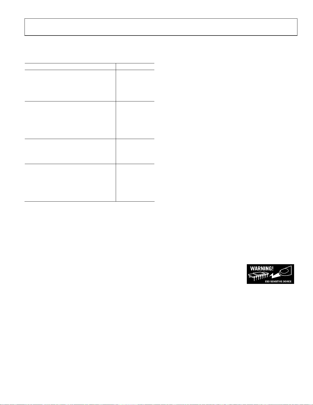
Table 2.
Parameter Rating
Voltage
Supply Voltage (VPSn, VPSV, VPSL, VPOS) 5.5 V
Input Voltage (INHn) VS + 200 mV
ENB, ENBL, ENBV, HILO Voltage VS + 200 mV
GAIN Voltage 2.5 V
Power Dissipation
AR Package
1
0.96 W
CP-20 Package (AD8331) 1.63 W
CP-32 Package (AD8332) 1.97 W
RQ Package
1
0.78 W
CP-64 Package (AD8334) 0.91 W
Temperature
Operating Temperature Range −40°C to +85°C
Storage Temperature Range −65°C to +150°C
Lead Temperature (Soldering 60 sec) 300°C
θ
JA
AR Package
CP-20 Package
CP-32 Package
RQ Package
CP-64 Package
1
Four-layer JEDEC board (2S2P).
2
Exposed pad soldered to board, nine thermal vias in pad—JEDEC, 4-layer
board J-STD-51-9.
3
Exposed pad soldered to board, 25 thermal vias in pad—JEDEC, 4-layer
board J-STD-51-9.
1
2
2
1
3
68°C/W
40°C/W
33°C/W
83°C/W
24.2°C/W
Stresses above those listed under Absolute Maximum Ratings
may cause permanent damage to the device. This is a stress
rating only; functional operation of the device at these or any
other conditions above those indicated in the operational
section of this specification is not implied. Exposure to absolute
maximum rating conditions for extended periods may affect
device reliability.
ESD CAUTION
ESD (electrostatic discharge) sensitive device. Electrostatic charges as high as 4000 V readily accumulate on
the human body and test equipment and can discharge without detection. Although this product features
proprietary ESD protection circuitry, permanent damage may occur on devices subjected to high energy
electrostatic discharges. Therefore, proper ESD precautions are recommended to avoid performance
degradation or loss of functionality.
Rev. E | Page 7 of 40
AD8331/AD8332/AD8334
PIN CONFIGURATIONS AND FUNCTION DESCRIPTIONS
LMD
INH
VPSL
LON
LOP
COML
VIP
VIN
MODE
GAIN
1
2
3
4
5
6
(Not to Scale)
7
8
9
10
PIN 1
INDICAT OR
AD8331
TOP VIEW
20
19
18
17
16
15
14
13
12
11
COMM
ENBL
ENBV
COMM
VOL
VOH
VPOS
HILO
RCLMP
VCM
03199-003
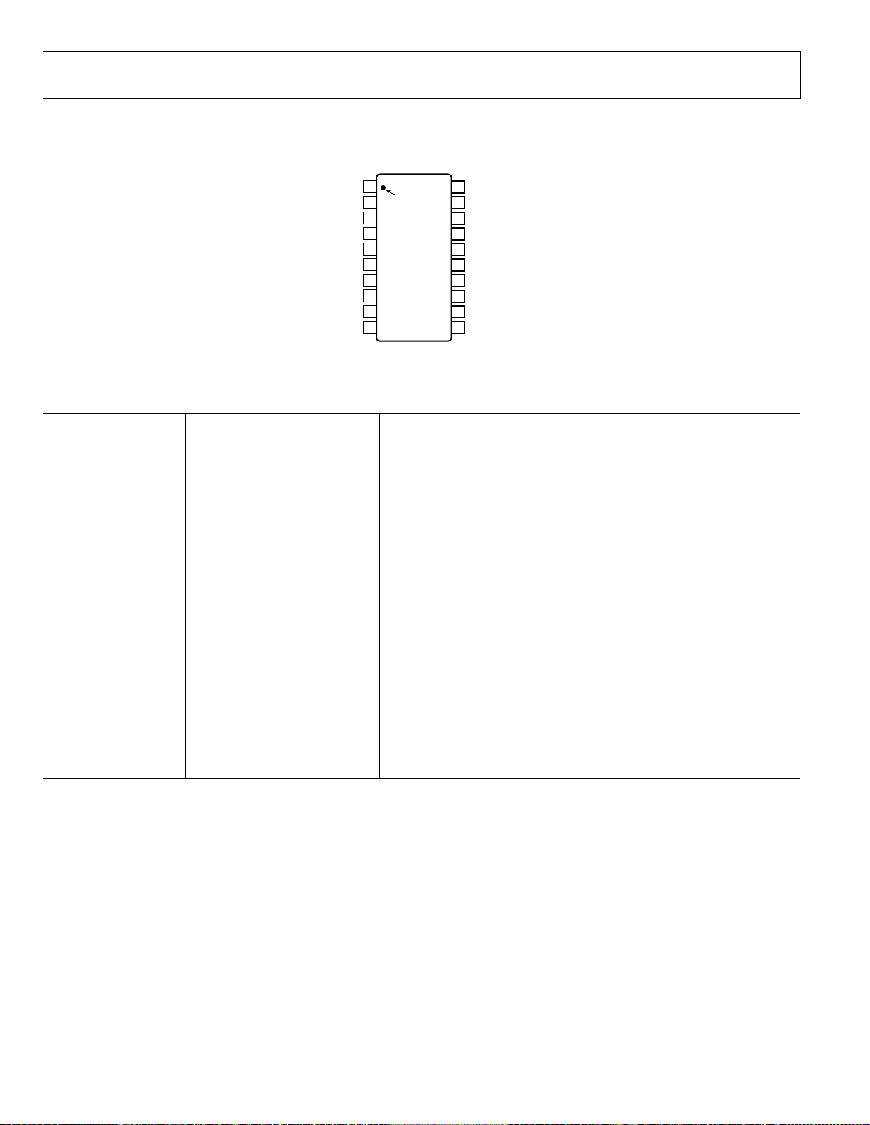
Figure 3. 20-Lead QSOP Pin Configuration (AD8331)
Table 3. 20-Lead QSOP Pin Function Description (AD8331)
Pin No. Mnemonic Description
1 LMD LNA Signal Ground
2 INH LNA Input
3 VPSL LNA 5 V Supply
4 LON LNA Inverting Output
5 LOP LNA Noninverting Output
6 COML LNA Ground
7 VIP VGA Noninverting Input
8 VIN VGA Inverting Input
9 MODE Gain Slope Logic Input
10 GAIN Gain Control Voltage
11 VCM Common Mode Voltage
12 RCLMP Output Clamping Level
13 HILO Gain Range Select (HI or LO)
14 VPOS VGA 5 V Supply
15 VOH Noninverting VGA Output
16 VOL Inverting VGA Output
17 COMM VGA Ground
18 ENBV VGA Enable
19 ENBL LNA Enable
20 COMM VGA Ground
Rev. E | Page 8 of 40
AD8331/AD8332/AD8334
1
LMD2
INH2
VPS2
LON2
LOP2
COM2
VIP2
VIN2
VCM2
GAIN
RCLMP
VOH2
VOL2
COMM
2
3
4
5
6
7
(Not to Scale)
8
9
10
11
12
13
14
PIN 1
INDICATO R
AD8332
TOP VIEW
Figure 4. 28-Lead TSSOP Pin Configuration (AD8332)
28
LMD1
27
INH1
26
VPS1
25
LON1
24
LOP1
23
COM1
22
VIP1
21
VIN1
20
VCM1
19
HILO
18
ENB
17
VOH1
16
VOL1
15
VPSV
03199-004
LON1
VPS1
INH1
LMD1
LMD2
INH2
VPS2
LON2
NC = NO CONNECT
1
2
3
4
5
6
7
8
LOP1
COM1
PIN 1
INDICATO R
LOP2
COM2
VIP1
VIN1
VCM1
29303132 28 252627
AD8332
TOP VIEW
(Not to Scale)
VIP2
VIN2
VCM2
HILO
ENBL
ENBV
COMM
24
VOH1
23
VOL1
22
VPSV
21
20
NC
19
VOL2
18
VOH2
17
14139121110
15 16
GAIN
MODE
COMM
RCLMP
03199-005
Figure 5. 32-Lead LFCSP Pin Configuration (AD8332)
Table 4. 28-Lead TSSOP Pin Function Description (AD8332)
Pin No. Mnemonic Description
1 LMD2 CH2 LNA Signal Ground
2 INH2 CH2 LNA Input
3 VPS2 CH2 Supply LNA 5 V
4 LON2 CH2 LNA Inverting Output
5 LOP2 CH2 LNA Noninverting Output
6 COM2 CH2 LNA Ground
7 VIP2 CH2 VGA Noninverting Input
8 VIN2 CH2 VGA Inverting Input
9 VCM2 CH2 Common-Mode Voltage
10 GAIN Gain Control Voltage
11 RCLMP Output Clamping Resistor
12 VOH2 CH2 Noninverting VGA Output
13 VOL2 CH2 Inverting VGA Output
14 COMM VGA Ground (Both Channels)
15 VPSV VGA Supply 5 V (Both Channels)
16 VOL1 CH1 Inverting VGA Output
17 VOH1 CH1 Noninverting VGA Output
18 ENB Enable—VGA/LNA
19 HILO VGA Gain Range Select (HI or LO)
20 VCM1 CH1 Common-Mode Voltage
21 VIN1 CH1 VGA Inverting Input
22 VIP1 CH1 VGA Noninverting Input
23 COM1 CH1 LNA Ground
24 LOP1 CH1 LNA Noninverting Output
25 LON1 CH1 LNA Inverting Output
26 VPS1 CH1 LNA Supply 5 V
27 INH1 CH1 LNA Input
28 LMD1 CH1 LNA Signal Ground
Table 5. 32-Lead LFCSP Pin Function Description (AD8332)
Pin No. Mnemonic Description
1 LON1 CH1 LNA Inverting Output
2 VPS1 CH1 LNA Supply 5 V
3 INH1 CH1 LNA Input
4 LMD1 CH1 LNA Signal Ground
5 LMD2 CH2 LNA Signal Ground
6 INH2 CH2 LNA Input
7 VPS2 CH2 LNA Supply 5 V
8 LON2 CH2 LNA Inverting Output
9 LOP2 CH2 LNA Noninverting Output
10 COM2 CH2 LNA Ground
11 VIP2 CH2 VGA Noninverting Input
12 VIN2 CH2 VGA Inverting Input
13 VCM2 CH2 Common-Mode Voltage
14 MODE Gain Slope Logic Input
15 GAIN Gain Control Voltage
16 RCLMP Output Clamping Level Input
17 COMM VGA Ground
18 VOH2 CH2 Noninverting VGA Output
19 VOL2 CH2 Inverting VGA Output
20 NC No Connect
21 VPSV VGA Supply 5 V
22 VOL1 CH1 Inverting VGA Output
23 VOH1 CH1 Noninverting VGA Output
24 COMM VGA Ground
25 ENBV VGA Enable
26 ENBL LNA Enable
27 HILO VGA Gain Range Select (HI or LO)
28 VCM1 CH1 Common-Mode Voltage
29 VIN1 CH1 VGA Inverting Input
30 VIP1 CH1 VGA Noninverting Input
31 COM1 CH1 LNA Ground
32 LOP1 CH1 LNA Noninverting Output
Rev. E | Page 9 of 40
AD8331/AD8332/AD8334
COM2
COM1
INH1
LMD1
COM1X
LON1
LOP1
VIP1
VIN1
VPS1
GAIN12
CLMP12
EN12
EN34
VCM1
VCM2
LMD4
COM4X
58 5764 63 5962 61 60
AD8334
TOP VIEW
(Not to Scale)
VIP4
VIN4
LOP4
LON4
VPS4
2825 26 272017 18 19 21 22 23 24
GAIN34
CLMP34
29 30 31 32
HILO
VCM4
INH2
1
LMD2
LON2
LOP2
VIP2
VIN2
VPS2
VPS3
VIN3
VIP3
LOP3
LON3
LMD3
INH3
2
3
4
5
6
7
8
9
10
11
12
13
14
15
16
COM3
COM2X
COM3X
NC = NO CONNECT
PIN 1
INDICATO R
INH4
COM4
Figure 6. 64-Lead LFCSP Pin Configuration (AD8334)
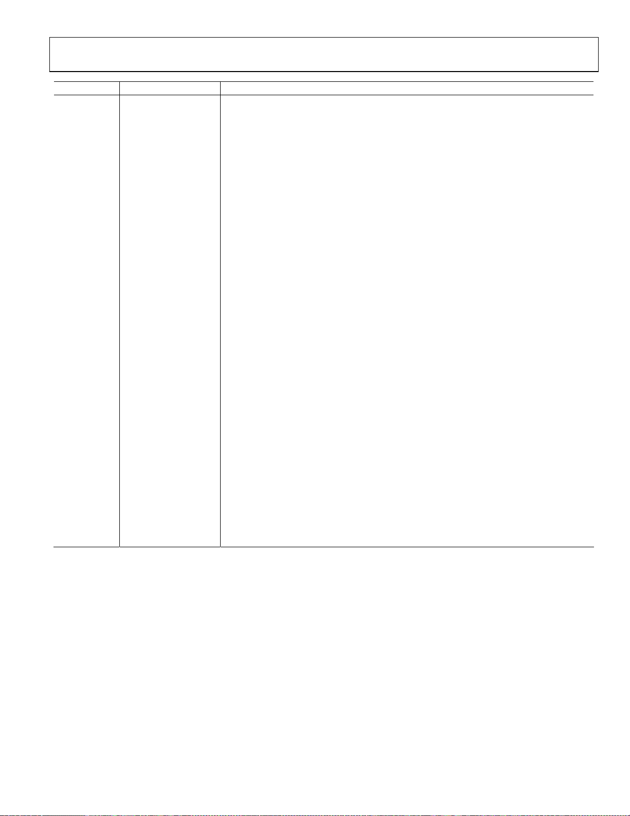
Table 6. 64-Lead LFCSP Pin Function Description (AD8334)
Pin No. Mnemonic Description
1 INH2 CH2 LNA Input
2 LMD2 CH2 LNA V
Bypass (AC-Coupled to GND)
MID
3 COM2X CH2 LNA Ground Shield
4 LON2 CH2 LNA Feedback Output (for R
FBK
)
5 LOP2 CH2 LNA Output
6 VIP2 CH2 VGA Positive Input
7 VIN2 CH2VGA Negative Input
8 VPS2 CH2 LNA Supply 5 V
9 VPS3 CH3 LNA Supply 5 V
10 VIN3 CH3VGA Negative Input
11 VIP3 CH3 VGA Positive Input
12 LOP3 CH3 LNA Positive Output
13 LON3 CH3 LNA Feedback Output (for R
FBK
)
14 COM3X CH3 LNA Ground Shield
15 LMD3 CH3 LNA V
Bypass (AC-Coupled to GND)
MID
16 INH3 CH3 LNA Input
17 COM3 CH3 LNA Ground
18 COM4 CH4 LNA Ground
19 INH4 CH4 LNA Input
20 LMD4 CH4 LNA V
Bypass (AC-Coupled to GND)
MID
21 COM4X CH4 LNA Ground Shield
22 LON4 CH4 LNA Feedback Output (for R
FBK
)
23 LOP4 CH4 LNA Positive Output
24 VIP4 CH4 VGA Positive Input
25 VIN4 CH4VGA Negative Input
26 VPS4 CH4 LNA Supply 5 V
27 GAIN34 Gain Control Voltage for CH3 and CH4
28 CLMP34 Output Clamping Level Input for CH3 and CH4
50 4956 55 5154 53 52
48
COM12
47
VOH1
46
VOL1
45
VPS12
44
VOL2
43
VOH2
42
COM12
41
MODE
40
NC
NC
39
COM34
38
VOH3
37
VOL3
36
VPS34
35
VOL4
34
VOH4
33
COM34
NC
VCM3
03199-006
Rev. E | Page 10 of 40
AD8331/AD8332/AD8334
Pin No. Mnemonic Description
29 HILO Gain Select for Postamp 0 dB or 12 dB
30 VCM4 CH4 Common-Mode Voltage—AC Bypass
31 VCM3 CH3 Common-Mode Voltage—AC Bypass
32 NC No Connect
33 COM34 VGA Ground, CH3 and CH4
34 VOH4 CH4 Positive VGA Output
35 VOL4 CH4 Negative VGA Output
36 VPS34 VGA Supply 5V CH3 and CH4
37 VOL3 CH3 Negative VGA Output
38 VOH3 CH3 Positive VGA Output
39 COM34 VGA ground CH3 and CH4
40 NC No Connect
41 MODE Gain Control SLOPE, Logic Input, 0 = Positive
42 COM12 VGA Ground CH1 and CH2
43 VOH2 CH2 Positive VGA Output
44 VOL2 CH2 Negative VGA Output
45 VPS12 CH2 VGA Supply 5 V CH1 and CH2
46 VOL1 CH1 Negative VGA Output
47 VOH1 CH1 Positive VGA Output
48 COM12 VGA Ground CH1 and CH2
49 VCM2 CH2 Common-Mode Voltage—AC Bypass
50 VCM1 CH1 Common-Mode Voltage—AC Bypass
51 EN34 Shared LNA/VGA Enable, CH3 and CH4
52 EN12 Shared LNA/VGA Enable, CH1 and CH2
53 CLMP12 Output Clamping Level Input, CH1 and CH2
54 GAIN12 Gain Control Voltage CH1 and CH2
55 VPS1 CH1 LNA Supply 5 V
56 VIN1 CH1 VGA Negative Input
57 VIP1 CH1 VGA Positive Input
58 LOP1 CH1 LNA Positive Output
59 LON1 CH1 LNA Feedback Output (for R
60 COM1X CH1 LNA Ground Shield
61 LMD1 CH1 LNA V
Bypass (AC-Coupled to GND)
MID
62 INH1 CH1 LNA Input
63 COM1 CH1 LNA Ground
64 COM2 CH2 LNA Ground
FBK
)
Rev. E | Page 11 of 40
AD8331/AD8332/AD8334
TYPICAL PERFORMANCE CHARACTERISTICS
TA = 25°C, VS = 5 V, RL = 500 Ω, RS = RIN = 50 Ω, RFB = 280 Ω, CSH = 22 pF, f = 10 MHz, R
−4.5 dB to +43.5 dB gain (HILO = LO), and differential output voltage, unless otherwise specified.
60
50
40
30
20
GAIN (dB)
10
0
–10
0 0.2 0.4 0.6 0.8 1.0 1.1
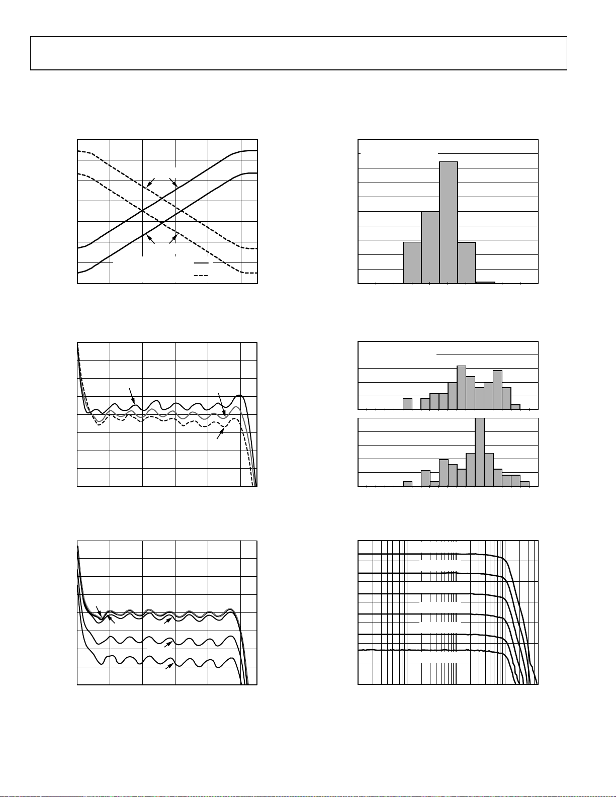
Figure 7. Gain vs. V
ASCENDING GAIN MODE
DESCENDI NG GAI N MODE
(WHERE AVAILABLE)
GAIN
HILO = HI
HILO = LO
V
(V)
GAIN
and MODE (MODE Available on AC Package)
2.0
1.5
1.0
0.5
0
–0.5
GAIN ERROR (dB)
–1.0
–1.5
–2.0
0 0.2 0.4 0.6 0.8 1.0 1.1
Figure 8. Absolute Gain Error vs. V
2.0
1.5
1.0
0.5
0
–0.5
GAIN ERROR (dB)
–1.0
–1.5
–2.0
0 0.2 0.4 0.6 0.8 1.0 1.1
Figure 9. Absolute Gain Error vs. V
1MHz
–40°C
10MHz
V
GAIN
30MHz
50MHz
70MHz
V
GAIN
(V)
at Three Temperatures
GAIN
(V)
at Various Frequencies
GAIN
03199-007
+25°C
+85°C
03199-008
03199-009
50
40
30
20
PERCENT OF UNI TS (%)
10
0
–0.5 –0.4 –0. 3 –0.2 –0. 1 0 0.1 0. 2 0.3 0.4 0.5
25
20
15
10
5
0
25
20
15
PERCENT OF UNI TS (%)
10
5
0
Figure 11. Gain Match Histogram for V
50
40
30
20
10
GAIN (dB)
0
–10
–20
100k 1M 10M 100M 500M
Figure 12. Frequency Response for Various Values of V
= ∞, CL = 1 pF, VCM pin floating,
CLMP
SAMPLE SIZE = 80 UNITS
V
= 0.5V
GAIN
GAIN ERROR (dB)
Figure 10. Gain Error Histogram
SAMPLE SIZE = 50 UNITS
V
= 0.2V
GAIN
V
= 0.7V
GAIN
0.01
–0.17
–0.15
–0.13
–0.11
–0.09
–0.07
CHANNEL TO CHANNEL G AIN MATCH (d B)
–0.05
V
V
V
V
V
V
FREQUENCY (Hz)
–0.03
GAIN
GAIN
GAIN
GAIN
GAIN
GAIN
–0.01
= 1V
= 0.8V
= 0.6V
= 0.4V
= 0.2V
= 0V
0.03
0.05
0.07
0.09
0.11
= 0.2 V and 0.7 V
GAIN
03199-010
03199-011
0.13
0.15
0.17
0.19
0.21
03199-012
GAIN
Rev. E | Page 12 of 40
 Loading...