Analog Devices AD8330 b Datasheet
Low Cost DC-150 MHz
Variable Gain Amplifier
FEATURES
Fully Differential Signal Path
May also be Used with Single-Sided Signals
Inputs from 0.3 mV to 1 V rms, Rail-to-Rail Outputs
Differential R
= 1 k; R
IN
(Each Output) 75
OUT
Automatic Offset Compensation (Optional)
Linear-in-dB and Linear-in-Magnitude Gain Modes
0 dB to 50 dB, for 0 V < V
< 1.5 V (30 mV/dB)
DBS
Inverted Gain Mode: 50 dB to 0 dB at –30 mV/dB
0.03 to 10 Nominal Gain for 15 mV < V
MAG
< 5 V
Constant Bandwidth: 150 MHz at All Gains
Low Noise: 5 nV/√Hz Typical at Maximum Gain
Low Distortion: ≤–62 dBc Typ
Low Power: 20 mA Typ at V
of 2.7 V – 6 V
S
Available in Space-Saving 3 3 LFCSP Package
APPLICATIONS
Pre-ADC Signal Conditioning
75 Cable Driving Adjust
AGC Amplifiers
GENERAL DESCRIPTION
The AD8330 is a wideband variable gain amplifier for use in
applications requiring a fully differential signal path, low noise, welldefined gain, and moderately low distortion, from dc to 150 MHz.
The input pins can also be driven from a single ended source. The
peak differential input is ±2V, allowing sine wave operation at
1V rms with generous headroom. The output pins can optionally
drive single-sided loads and each swing essentially rail-to-rail.
The differential output resistance is 150 Ω. The output swing is
a linear function of the voltage applied to the VMAG pin, which
internally defaults to 0.5 V, to provide a peak output of ±2 V.
This may be raised to 10 V p-p, limited by the supply voltage.
The basic gain function is linear-in-dB, controlled by the voltage
applied to pin VDBS. The gain ranges from 0 dB to 50 dB for
control voltages between 0 V and 1.5 V—a slope of 30 mV dB.
The gain linearity is typically within ±0.1 dB. By changing the
logic level on pin MODE, the gain will decrease over the same
range, with opposite slope. A second gain control port is provided
at pin VMAG and allows the user to vary the numeric gain from a
factor of 0.03 to 10. All the parameters of the AD8330 have low
sensitivities to temperature and supply voltages.
Using V
, the basic 0 dB to 50 dB range can be repositioned to any
MAG
value from 20 dB higher (that is, 20 dB to 70 dB) to at least 30 dB
lower (that is, –30 dB to +20 dB) to suit the application, providing
an unprecedented gain range of over 100 dB. A unique aspect of
the AD8330 is that its bandwidth and pulse response are essentially
constant for all gains, not only over the basic 50 dB linear-in-dB
*Protected by U.S.Patent No. 5,969,657; other patents pending.
REV. B
Information furnished by Analog Devices is believed to be accurate and
reliable. However, no responsibility is assumed by Analog Devices for its
use, nor for any infringements of patents or other rights of third parties that
may result from its use. No license is granted by implication or otherwise
under any patent or patent rights of Analog Devices. Trademarks and
registered trademarks are the property of their respective owners.
AD8330
*
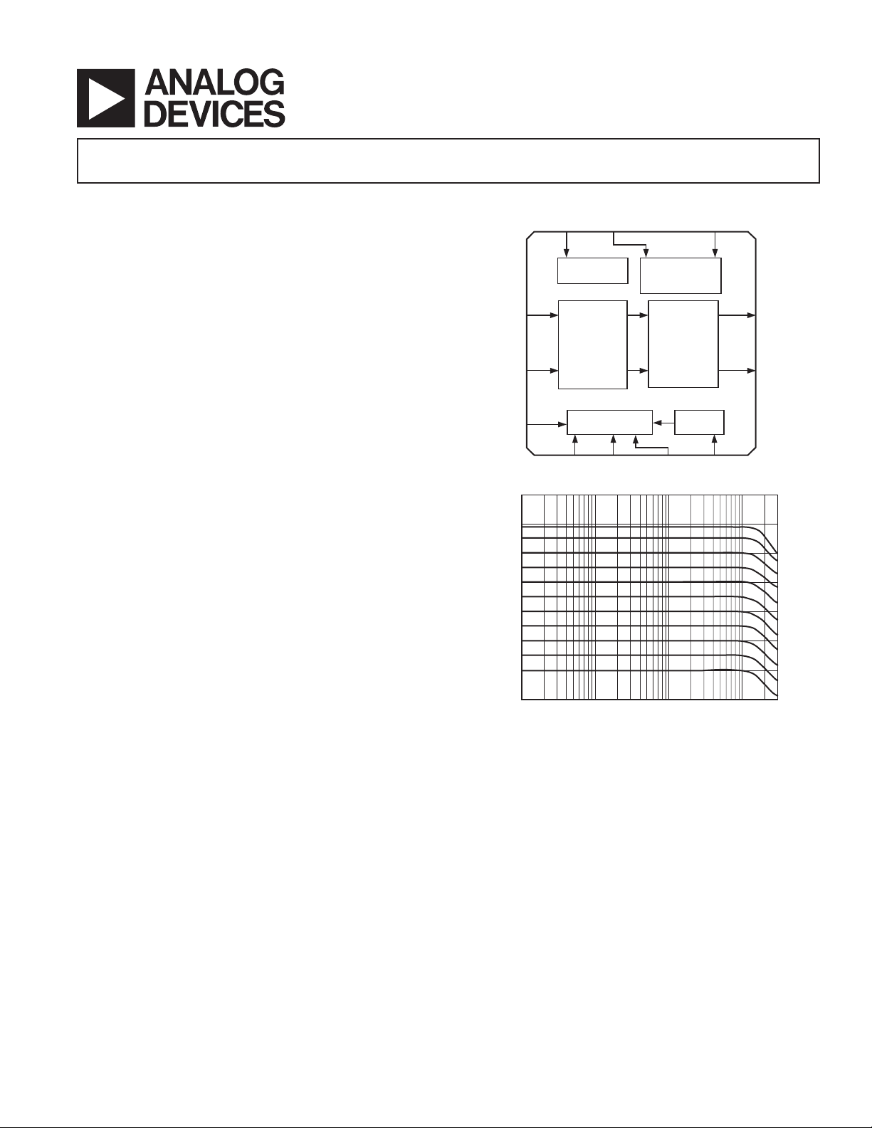
FUNCTIONAL BLOCK DIAGRAM
16 15 14 13
OFSTENBL CNTRVPOS
1
VPSI
INHI
2
INLO
3
MODE
4
90
70
50
30
10
GAIN – dB
–10
–30
–50
100k
BIAS AND V
VDBS CMGN VMAG
5678
REF
VGA CORE
GAIN INTERFACE
1M 10M 100M 300M
FREQUENCY – Hz
CM AND
OFFSET
CONTROL
OUTPUT
STAGES
OUTPUT
CONTROL
COMM
VPSO
OPHI
OPLO
CMOP
12
11
10
9
Figure 1. AC Response over the Extended Gain Range
range, but also when using the linear-in-magnitude function. The
exceptional stability of the HF response over the gain range is of
particular value in those VGA applications where it is essential
to maintain accurate gain law-conformance at high frequencies.
An external capacitor at pin OFST sets the high-pass corner of an
offset reduction loop, whose frequency may be as low as 5 Hz.
When this pin is grounded, the signal path becomes dc-coupled.
When used to drive an ADC, an external common-mode control
voltage at pin CNTR can be driven to within 0.5 V of either
ground or V
to accommodate a wide variety of requirements. By
S
default, the two outputs are positioned at the midpoint of the
supply, V
/2. Other features, such as two levels of power-down
S
(fully off and a hibernate mode), further extend the practical
value of this exceptionally versatile VGA.
The AD8330 is available in 16-lead LFCSP and 16-lead QSOP
packages and is specified for operation from –40°C to +85°C.
One Technology Way, P.O. Box 9106, Norwood, MA 02062-9106, U.S.A.
Tel: 781/329-4700 www.analog.com
Fax: 781/326-8703 © 2004 Analog Devices, Inc. All rights reserved.

AD8330–SPECIFICATIONS
(VS = 5 V, TA = 25C, CL = 12 pF on OPHI and OPLO, RL = 0/C, V
V
MAG
= 0/C, V
= 0 V, Differential Operation, unless otherwise noted.)
OFST
= 0.75 V, V
DBS
MODE
= HI,
Parameter Conditions Min Typ Max Unit
INPUT INTERFACE Pins INHI, INLO
Full-Scale Input V
= 0 V, Differential Drive ±1.4 ± 2V
DBS
V
= 1.5 V ±4.5 ± 6.3 mV
DBS
Input Resistance Pin-to-Pin 800 1k 1.2k Ω
Input Capacitance Either Pin to COMM 4 pF
Voltage Noise Spectral Density f = 1 MHz, V
= 1.5 V; 5 nV/√Hz
DBS
Inputs ac-shorted
Common-Mode Voltage Level 3.0 V
Input Offset Pin OFST Connected to COMM 1 mV rms
Drift 2 µV/°C
Permissible CM Range
1
0V
S
V
Common-Mode AC Rejection f = 1 MHz, 0.1 V rms –60 dB
f = 50 MHz –55 dB
OUTPUT INTERFACE Pins OPHI, OPLO
Small Signal –3 dB Bandwidth 0 V < V
Peak Slew Rate V
DBS
< 1.5 V 150 MHz
DBS
= 0 1500 V/µs
Peak-to-Peak Output Swing ±1.8 ± 2 ± 2.2 V
≥ 2 V (Peaks are Supply Limited) ±4 ±4.5 V
V
MAG
Common-Mode Voltage Pin CNTR O/C 2.4 2.5 2.6 V
Voltage Noise Spectral Density f = 1 MHz, V
Differential Output Impedance Pin-to-Pin 120 150 180 Ω
HD2
HD3
2
2
V
= 1 V p-p, f = 10 MHz, RL = 1 kΩ –62 dBc
OUT
V
= 1 V p-p, f = 10 MHz, RL = 1 kΩ –53 dBc
OUT
= 0 62 nV/√Hz
DBS
OUTPUT OFFSET CONTROL Pin OFST
AC-Coupled Offset C
High-Pass Corner Frequency C
on Pin OFST (0 V< V
HPF
= 3.3 nF, from OFST 100 kHz
HPF
to CNTR (Scales as 1/C
< 1.5 V) 10 mV rms
DBS
)
HPF
COMMON-MODE CONTROL Pin CNTR
Usable Voltage Range 0.5 4.5 V
Input Resistance From Pin CNTR to VS/2 4 kΩ
DECIBEL GAIN CONTROL Pins VDBS, CMGN, MODE
Normal Voltage Range CMGN Connected to COMM 0 to 1.5 V
Elevated Range CMGN O/C (V
Rises to 0.2 V) 0.2 to 1.7 V
CMGN
Gain Scaling Mode HIGH or LOW 27 30 33 mV/dB
Gain Linearity Error 0.3 V ≤ V
Absolute Gain Error V
= 0 –2 ± 0.5 +2 dB
DBS
≤ 1.2 V –0.35 ± 0.1 +0.35 dB
DBS
Bias Current Flows out of pin VDBS 100 nA
Incremental Resistance 100 MΩ
Gain Settling Time to 0.5 dB Error V
Stepped from 0.05 V–1.45 V 250 ns
DBS
or 1.45 V–0.05 V
Mode Up/Down Pin MODE
Mode Up Logic Level Gain Increases with V
Mode Down Logic Level Gain Decreases with V
, MODE = O/C 1.5 V
DBS
DBS
0.5 V
LINEAR GAIN INTERFACE Pins VMAG, CMGN
Peak Output Scaling, Gain vs. V
Gain Multiplication Factor vs. V
See Circuit Description Section 3.8 4.0 4.2 V/V
MAG
Gain is Nominal when V
MAG
= 0.5 V ⫻2
MAG
Usable Input Range 0 5 V
Default Voltage V
O/C 0.48 0.5 0.52 V
MAG
Incremental Resistance 4kΩ
Bandwidth For V
≥ 0.1 V 150 MHz
MAG
REV. B–2–

AD8330
Parameter Conditions Min Typ Max Unit
CHIP ENABLE Pin ENBL
Logic Voltage for Full Shutdown 0.5 V
Logic Voltage for Hibernate Mode Output Pins Remain at CNTR 1.3 1.5 1.7 V
Logic Voltage for Full Operation 2.3 V
Current in Full Shutdown 20 100 µA
Current in Hibernate Mode 1.5 mA
Minimum Time Delay
POWER SUPPLY Pins VPSI, VPOS, VPSO,
Supply Voltage 2.7 6 V
Quiescent Current V
NOTES
1
The use of an input common-mode voltage significantly different than the internally set value is not recommended due to its effect on noise performance.
See Figure 13.
2
See Typical Performance Characteristics for more detailed information on distortion in a variety of operating conditions.
3
For minimum sized coupling capacitors.
3
1.7 µs
COMM, CMOP
= 0.75 V 20 27 mA
DBS
REV. B
–3–
AD8330
ABSOLUTE MAXIMUM RATINGS
1
Supply Voltage . . . . . . . . . . . . . . . . . . . . . . . . . . . . . . . . . . . 6 V
Power Dissipation
RQ Package
2
. . . . . . . . . . . . . . . . . . . . . . . . . . . . . . 0.62 W
CP Package . . . . . . . . . . . . . . . . . . . . . . . . . . . . . . . .1.67 W
Input Voltage at Any Pin . . . . . . . . . . . . . . . . . . . V
+ 200 mV
S
Storage Temperature . . . . . . . . . . . . . . . . . . . –65°C to +105°C
JA
RQ-16 Package . . . . . . . . . . . . . . . . . . . . . . . . . 105.4°C/W
CP-16 Package . . . . . . . . . . . . . . . . . . . . . . . . . . . . . 60°C/W
JC
RQ-16 Package . . . . . . . . . . . . . . . . . . . . . . . . . . . . 39°C/W
ORDERING GUIDE
Model Temperature Range Package Description Package Option Branding
AD8330ACP-R2 –40°C to +85°C LFCSP CP-16-3 JFA
AD8330ACP-REEL –40°C to +85°C LFCSP CP-16-3 JFA
AD8330ACP-REEL7 –40°C to +85°C LFCSP CP-16-3 JFA
AD8330ACPZ-R2* –40°C to +85°C LFCSP CP-16-3 JFA
AD8330ACPZ-REEL* –40°C to +85°C LFCSP CP-16-3 JFA
AD8330ACPZ-REEL7*
–40°C to +85°C LFCSP CP-16-3 JFA
AD8330ARQ –40°C to +85°C QSOP RQ-16
AD8330ARQ-REEL –40°C to +85°C QSOP RQ-16
AD8330ARQ-REEL7 –40°C to +85°C QSOP RQ-16
AD8330ARQZ* –40°C to +85°C QSOP RQ-16
AD8330ARQZ-REEL* –40°C to +85°C QSOP RQ-16
AD8330ARQZ-REEL7*
–40°C to +85°C QSOP RQ-16
AD8330-EVAL Evaluation Board
*Z = Pb-free part.
Operating Temperature Range . . . . . . . . . . . . –40°C to +85°C
Lead Temperature (Soldering 60 sec) . . . . . . . . . . . . . . 300°C
NOTES
1
Stresses above those listed under Absolute Maximum Ratings may cause
permanent damage to the device. This is a stress rating only and functional
operation of the device at these or any other conditions above those indicated
in the operational section of this specification is not implied. Exposure to absolute
maximum rating conditions for extended periods may affect device reliability.
2
Four-Layer JEDEC Board (252P).
CAUTION
ESD (electrostatic discharge) sensitive device. Electrostatic charges as high as 4000 V readily
accumulate on the human body and test equipment and can discharge without detection. Although the
AD8330 features proprietary ESD protection circuitry, permanent damage may occur on devices
subjected to high energy electrostatic discharges. Therefore, proper ESD precautions are
recommended to avoid performance degradation or loss of functionality.
REV. B–4–
16-Lead LFCSP
AD8330
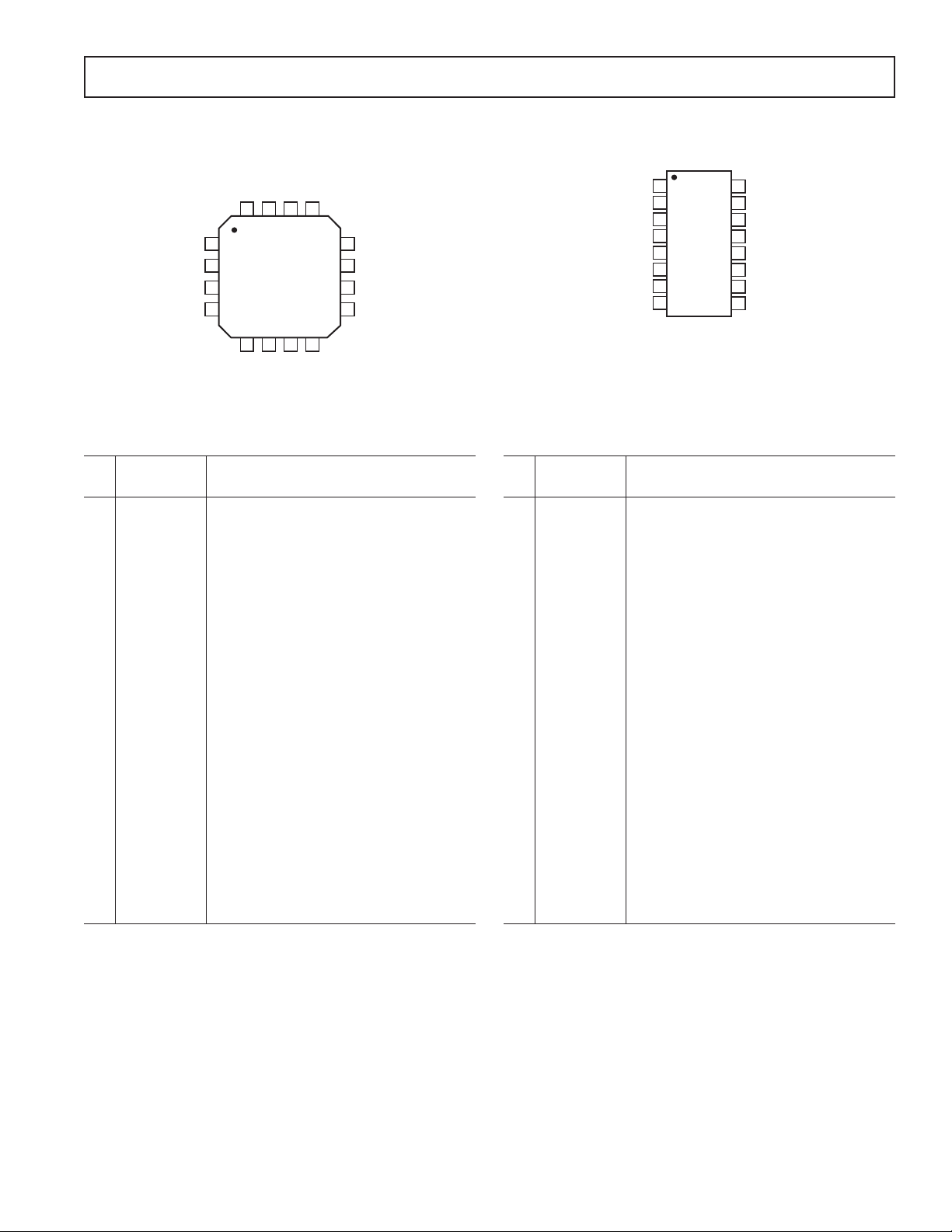
PIN CONFIGURATIONS
16-Lead QSOP
ENBL
OFST
VPOS
14
CMGN
13
COMM
CNTR
VMAG
12
11
10
9
VPSO
OPHI
OPLO
CMOP
VSPI
INHI
INLO
MODE
16
1
2
3
4
5678
VDBS
15
AD8330
TOP VIEW
(Not to Scale)
PIN FUNCTION DESCRIPTIONS
16-Lead LFCSP
Pin
No. Mnemonic Description
1 VPSI Positive Supply for Input Stages
2 INHI Differential Signal Input, Positive Polarity
3 INLO Differential Signal Input, Negative Polarity
4 MODE Logic Input: Selects Gain Slope. High =
Gain Up versus V
DBS
5 VDBS Input for Linear-in-dB Gain Control
Voltage, V
DBS
6 CMGN Common Baseline for Gain Control Interfaces
7 COMM Ground for Input and Gain Control Bias
Circuitry
8 VMAG Input for Gain/Amplitude Control, V
MAG
9 CMOP Ground for Output Stages
10 OPLO Differential Signal Output, Negative Polarity
11 OPHI Differential Signal Output, Positive Polarity
12 VPSO Positive Supply for Output Stages
13 CNTR Common-Mode Output Voltage Control
14 VPOS Positive Supply for Inner Stages
15 OFST Used in Offset Control Modes
16 ENBL Power Enable, Active High
1
OFST VPOS
2
ENBL CNTR
3
VPSI VPSO
INLO OPLO
MODE CMOP
VDBS VMAG
CMGN COMM
AD8330
4
INHI OPHI
TOP VIEW
(Not to Scale)
5
6
7
8
16
15
14
13
12
11
10
9
16-Lead QSOP
Pin
No. Mnemonic Description
1 OFST Used in Offset Control Modes
2 ENBL Power Enable, Active High
3 VPSI Positive Supply for Input Stages
4 INHI Differential Signal Input, Positive Polarity
5 INLO Differential Signal Input, Negative Polarity
6 MODE Logic Input: Selects Gain Slope. High =
Gain Up versus V
DBS
7 VDBS Input for Linear-in-dB Gain Control
Voltage, V
DBS
8 CMGN Common Baseline for Gain Control Interfaces
9 COMM Ground for Input and Gain Control Bias
Circuitry
10 VMAG Input for Gain/Amplitude Control, V
MAG
11 CMOP Ground for Output Stages
12 OPLO Differential Signal Output, Negative Polarity
13 OPHI Differential Signal Output, Positive Polarity
14 VPSO Positive Supply for Output Stages
15 CNTR Common-Mode Output Voltage Control
16 VPOS Positive Supply for Inner Stages
REV. B
–5–
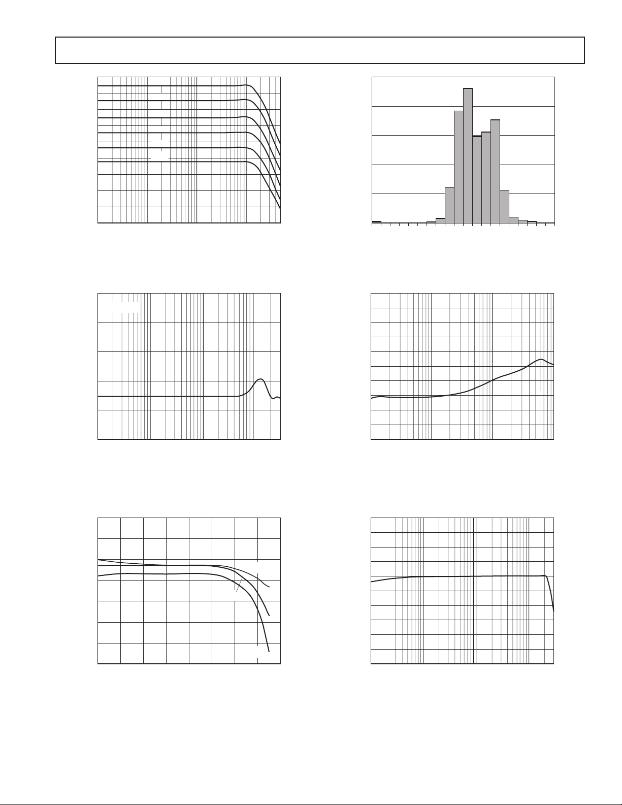
AD8330–Typical Performance Characteristics
VS = 5 V, TA = 25C, CL = 12 pF, V
50
45
40
35
30
25
GAIN – dB
20
15
10
5
0
0 0.25 0.50 1.00 1.25 1.50
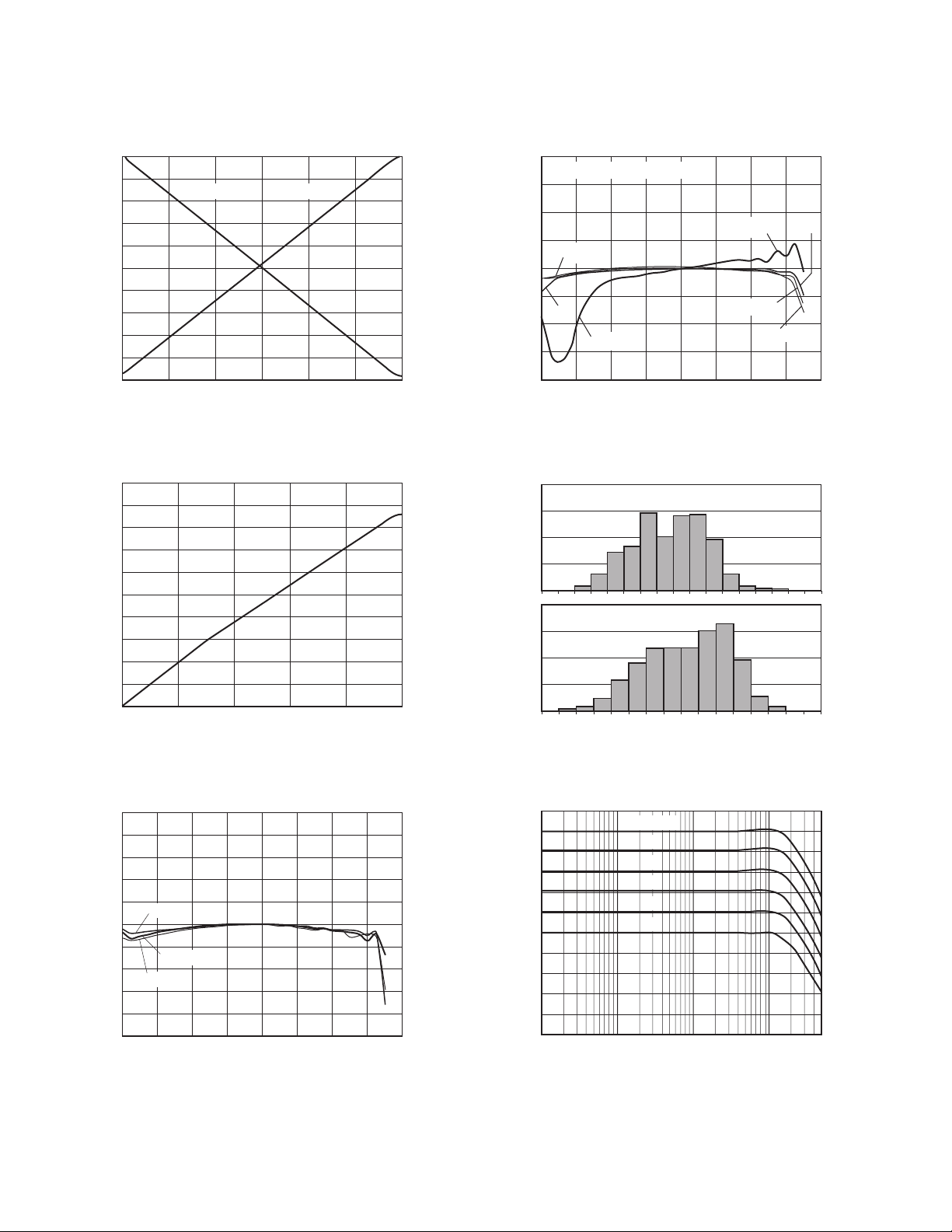
TPC 1. Gain vs. V
10
9
8
7
6
5
4
3
2
GAIN MULTIPLICATION FACTOR
1
0
01 345
= 0.75 V, V
DBS
0.75
V
DBS
2
V
MAG
– V
– V
= High (or O/C) V
MODE
HI MODELO MODE
DBS
= O/C, RL = O/C, V
MAG
= 0, Differential Operation, unless otherwise stated.
OFST
2.0
NORMALIZED @ V
1.5
1.0
0.5
10, 50MHz
0
–0.5
GAIN ERROR – dB
1MHz
–1.0
–1.5
–2.0
0 0.2 0.8 1.2 1.6
100MHz
0.4
TPC 4. Gain Error vs. V
20
2340 UNITS
MODE = LO
15
10
5
0
–30.6–30.5 –30.4 –30.3–30.2 –30.1–30.0 –29.9–29.8 –29.7–29.6 –29.5 –29.4–29.3 –29.2–29.1 –29.0
20
MODE = HI
% OF UNITS
15
10
5
0
29.1 29.2 29.3 29.4 29.5 29.6 29.7 29.8 29.9 30.0 30.1 30.2 30.3 30.4 30.5 30.6
= 0.75V
DBS
100MHz
1MHz
0.6 1.0 1.4
V
– V
DBS
at Various Frequencies
DBS
GAIN SCALING – mV/dB
50MHz
10MHz
TPC 2. Linear Gain Multiplication Factor vs. V
1.0
0.8
0.6
0.4
0.2
T = –40C
0
–0.2
GAIN ERROR – dB
–0.4
–0.6
–0.8
–1.0
T = +85C
T = +25C
0.6
0 0.2 1.0 1.4 1.6
0.8 1.20.4
V
– V
DBS
MAG
TPC 3. Gain Linearity Error Normalized at 25°C vs.
V
, at Three Temperatures, f = 1 MHz
DBS
TPC 5. Gain Slope Histogram
60
50
40
30
20
10
0
GAIN – dB
–10
–20
–30
–40
–50
100k
V
= 1.5V
DBS
1.2V
0.9V
0.6V
0.3V
0V
1M 10M 100M 500M
FREQUENCY – Hz
TPC 6. Frequency Response in 10 dB Steps for
Various Values of V
DBS
REV. B–6–
AD8330
FREQUENCY – Hz
10
100k
OUTPUT BALANCE – dB
–90
–70
–50
–30
–10
1M 10M 100M
0
–80
–60
–40
–20
FREQUENCY – Hz
200
100k
OUTPUT RESISTANCE –
100
120
140
160
180
1M 10M 300M
190
110
130
150
170
100M
50
40
30
20
10
0
GAIN – dB
–10
–20
–30
–40
100k
4.8V
1.52V
.48V
.15V
.048V
.015V
1M 10M 100M 500M
FREQUENCY – Hz
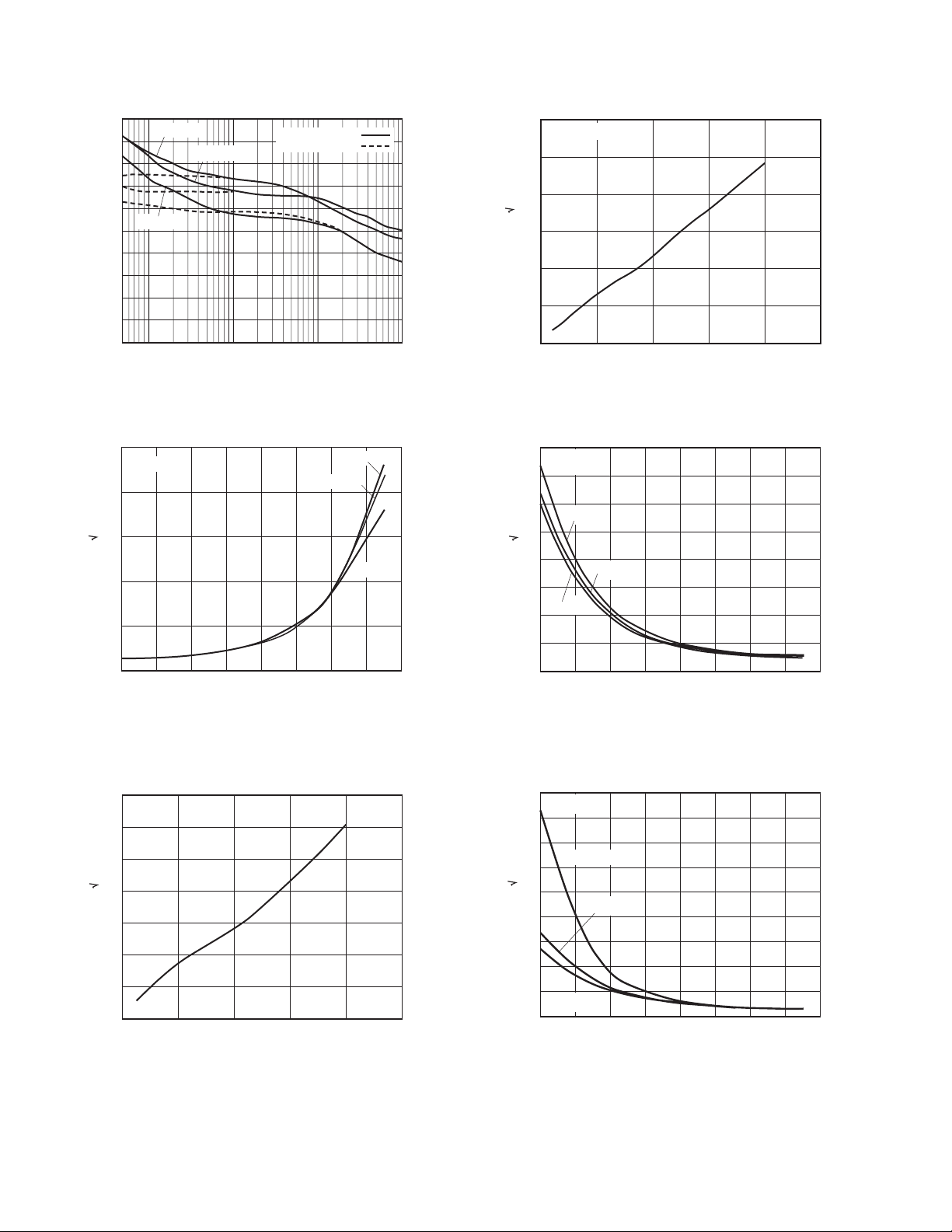
TPC 7. Frequency Response for Various Values of V
10
V
= 0.1V
DBS
8
6
MAG
25
1048 UNITS
ENABLE MODE
20
15
10
% OF UNITS
5
0
–0.9
–0.8
–0.7
–0.6
–0.5
–0.4
DIFFERENTIAL OFFSET – mV
–0.3
–0.2
–0.1
0
0.1
0.2
0.3
0.4
0.5
0.6
0.7
0.8
TPC 10. Differential Input Offset Histogram
0.9
1.0
4
GROUP DELAY – ns
2
0
100k
1M 10M 100M 300M
FREQUENCY – Hz
TPC 8. Group Delay vs. Frequency
0
–1
–2
–3
T = +25C
– V
OFFSET VOLTAGE – mV
–4
–5
–6
–7
0.2 0.4 0.6 0.8 1.0 1.2 1.4 1.6
0
V
DBS
TPC 9. Differential Output Offset vs. V
Three Temperatures, for a Representative Part
REV. B
T = –40C
T = +85C
DBS
for
TPC 11. Output Balance Error vs. Frequency for
a Representative Part
TPC 12. Output Impedance vs. Frequency
–7–
AD8330
90
V
= 1.5V
80
70
60
50
40
30
CMRR – dB
20
10
–10
DBS
= .75V
V
DBS
= 0V
V
DBS
0
50k
100k 1M 100M
FREQUENCY – Hz
OFST: ENABLED
DISABLED
10M
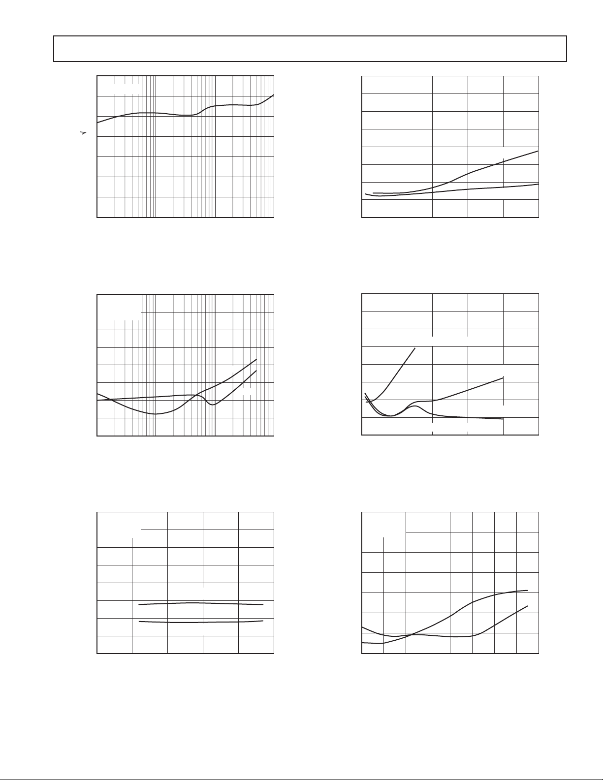
TPC 13. CMRR vs. Frequency
1500
f = 1MHz
1200
900
600
NOISE – nV/ Hz
300
T = +85C
T = +25C
T = –40C
6000
V
= 1.5V
DBS
f = 1MHz
5000
4000
3000
NOISE – nV/ Hz
2000
1000
0
0
0.5 1.0 2.51.5
V
– V
MAG
TPC 16. Output Referred Noise vs. V
80
V
= 0.5V
MAG
f = 1MHz
70
60
T = +85C
50
40
30
NOISE – nV/ Hz
20
10
T = +25C
T = –40C
2.0
MAG
0
0
0.2 0.4 0.6 0.8 1.0 1.2 1.4 1.6
VOLTA G E – V
TPC 14. Output Referred Noise vs. V
Three Temperatures
700
f = 1MHz
600
500
400
300
NOISE – nV/ Hz
200
100
0
0
0.5 1.0 2.51.5
V
– V
MAG
TPC 15. Output Referred Noise vs. V
2.0
DBS
for
MAG
0
0
0.2 0.4 0.6 0.8 1.0 1.2 1.4
V
– V
DBS
TPC 17. Input Referred Noise vs. V
Three Temperatures
180
f = 1MHz
160
140
V
= 0.125V
MAG
120
100
80
NOISE – nV/ Hz
60
40
20
0
0
V
= 0.5V
MAG
V
= 2V
MAG
0.2 0.4 0.6 0.8 1.0 1.2 1.4
V
– V
DBS
TPC 18. Input Referred Noise vs. V
Values of V
MAG
DBS
for Three
DBS
1.6
for
1.6
REV. B–8–
AD8330
V
OUT
– V p-p
0
0
DISTORTION – dBc
–80
–70
–60
–50
–20
1.5
–40
–10
–30
0.3 0.6 0.9 1.2
f = 10MHz
HD3, RL = 1k
HD2, RL = 1k
V
OUT
– V p-p
0
0
DISTORTION – dBc
–80
–70
–60
–50
–20
5
–40
–10
–30
1234
f = 10MHz
HD3, RL = 1k
HD2, RL = 1k
HD2 AND HD3, RL = 150*
*OUTPUT AMPLITUDE HARD LIMITED
V
DBS
– V
0
0
DISTORTION – dBc
–70
–60
–50
–20
1.6
–40
–10
–30
0.2 0.6 1.0 1.4
HD2
1.20.80.4
f = 10MHz
V
OUT
– 1V p-p
R
L
– 1k
HD3
7
V
= 1.5V
DBS
6
5
4
3
NOISE – nV/ Hz
2
1
0
100k
1M 10M
FREQUENCY – Hz
TPC 19. Input Referred Noise vs. Frequency
0
V
= 0.75V
DBS
= 1V p-p
V
OUT
–10
= 1k
R
L
–20
–30
–40
–50
DISTORTION – dBc
–60
–70
–80
100k
1M 10M
FREQUENCY – Hz
HD 3
HD 2
TPC 20. Harmonic Distortion vs. Frequency
100M
100M
TPC 22. Harmonic Distortion vs.
V
OUT-DIFFERENTIAL VMAG
= 0.5 V
TPC 23. Harmonic Distortion vs.
V
OUT-DIFFERENTIAL VMAG
= 2.0 V
–10
–20
–30
–40
–50
DISTORTION – dBc
REV. B
–60
–70
–80
0
V
= 0.75V
DBS
= 1V p-p
V
OUT
= 1k
R
L
HD 3
HD 2
0
TPC 21. Harmonic Distortion vs. C
10 20 30 40
C
LOAD
– pF
LOAD
50
TPC 24. Harmonic Distortion vs. V
DBS
–9–
 Loading...