ANALOG DEVICES AD8328 Service Manual

5 V Upstream
–
www.BDTIC.com/ADI
FEATURES
Supports DOCSIS and EuroDOCSIS standards for reverse
path transmission systems
Gain programmable in 1 dB steps over a 59 dB range
Low distortion at 60 dBmV output
−57.5 dBc SFDR at 21 MHz
−54 dBc SFDR at 65 MHz
Output noise level @ minimum gain 1.2 nV/√Hz
Maintains 300 Ω output impedance Tx-enable and
Tx-disable condition
Upper bandwidth: 107 MHz (full gain range)
5 V supply operation
Supports SPI interfaces
APPLICATIONS
DOCSIS and EuroDOCSIS cable modems
CATV set-top boxes
CATV telephony modems
Coaxial and twisted pair line drivers
Cable Line Driver
AD8328
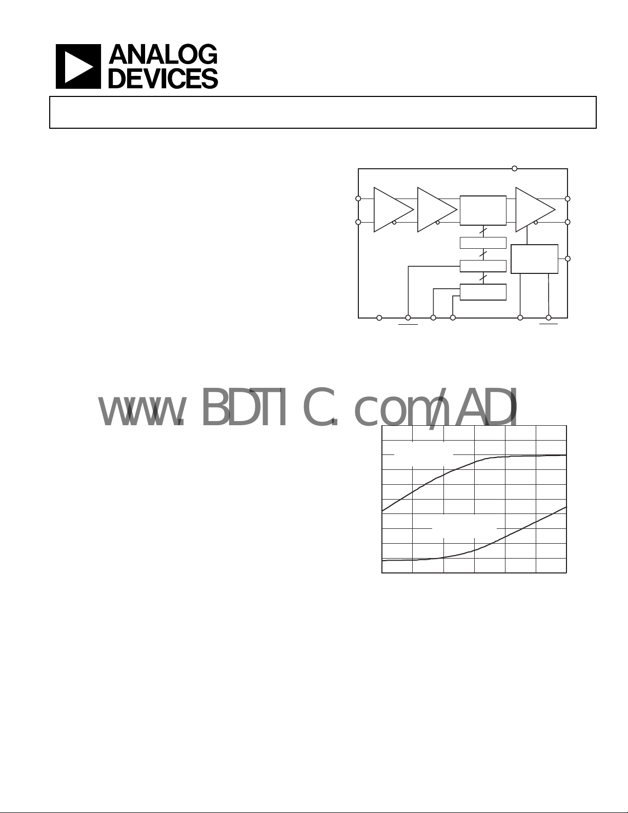
FUNCTIONAL BLOCK DIAGRAM
BYP
AD8328
IN+
IN–
DIFF
OR
SINGLE
INPUT
AMP
ZIN (SINGLE) = 800Ω
(DIFF) = 1.6kΩ
Z
IN
GND
VERNIER
DATEN
ATTENUATIO N
CORE
8
DECODE
8
DATA LATCH
8
SHIFT
REGISTER
SDATA CLK TXEN
POWER
POWER- DOWN
Figure 1.
AMP
Z
300Ω
LOGIC
OUT
SLEEP
DIFF =
V
OUT+
V
OUT–
RAMP
03158-001
V
V
GENERAL DESCRIPTION
The AD83281 is a low cost amplifier designed for coaxial line
driving. The features and specifications make the AD8328
ideally suited for MCNS-DOCSIS and EuroDOCSIS applications.
The gain of the AD8328 is digitally controlled. An 8-bit serial
word determines the desired output gain over a 59 dB range,
resulting in gain changes of 1 dB/LSB.
The AD8328 accepts a differential or single-ended input signal.
The o
utput is specified for driving a 75 Ω load through a 2:1
transformer.
Distortion performance of −53 dBc is achieved with an output
el up to 60 dBmV at 65 MHz bandwidth over a wide
lev
temperature range.
This device has a sleep mode function that reduces the quiescent
urrent to 2.6 mA and a full power-down function that reduces
c
power-down current to 20 µA.
The AD8328 is packaged in a low cost 20-lead LFCSP and
a 20-lead QSO
and has an operational temperature range of −40°C to +85°C.
P. The AD8328 operates from a single 5 V supply
50
–52
–54
–56
–58
–60
–62
DISTORTION (dBc)
–64
–66
–68
–70
5 152535455565
Figure 2. Worst Harmonic Distortion vs. Frequency
1
Patent pending.
V
= 60dBmV
OUT
@ MAX GAIN,
THIRD HARMONIC
V
OUT
@ MAX GAIN,
SECOND HARMONIC
= 60dBmV
FREQUENCY (MHz )
03158-002
Rev. A
Information furnished by Analog Devices is believed to be accurate and reliable. However, no
responsibility is assumed by Anal og Devices for its use, nor for any infringements of patents or ot her
rights of third parties that may result from its use. Specifications subject to change without notice. No
license is granted by implication or otherwise under any patent or patent rights of Analog Devices.
Trademarks and registered trademarks are the property of their respective owners.
One Technology Way, P.O. Box 9106, Norwood, MA 02062-9106, U.S.A.
Tel: 781.329.4700 www.analog.com
Fax: 781.461.3113 © 2005 Analog Devices, Inc. All rights reserved.

AD8328
www.BDTIC.com/ADI
TABLE OF CONTENTS
Features.............................................................................................. 1
Signal Integrity Layout Considerations................................... 11
Applications....................................................................................... 1
Functional Block Diagram ..............................................................1
General Description......................................................................... 1
Revision History ...............................................................................2
Specifications..................................................................................... 3
Logic Inputs (TTL-/CMOS-Compatible Logic)....................... 4
Timing Requirements.................................................................. 4
Absolute Maximum Ratings............................................................ 6
ESD Caution.................................................................................. 6
Pin Configurations and Function Descriptions........................... 7
Typical Performance Characteristics............................................. 8
Applications..................................................................................... 10
General Applications..................................................................10
Circuit Description.....................................................................10
SPI Programming and Gain Adjustment................................ 10
Initial Power-Up......................................................................... 12
RAMP Pin and BYP Pin Features............................................ 12
Transmit Enable (TXEN) and
Distortion, Adjacent Channel Power, and DOCSIS .............. 12
Noise and DOCSIS..................................................................... 12
Evaluation Board Features and Operation.............................. 12
Differential Signal Source ......................................................... 13
Differential Signal from Single-Ended Source....................... 13
Single-Ended Source.................................................................. 13
Overshoot on PC Printer Ports ................................................ 13
Installing Visual Basic Control Software................................. 13
Running AD8328 Software....................................................... 14
Controlling Gain/Attenuation of the AD8328....................... 14
Transmit Enable and Sleep Mode............................................. 14
Memory Functions..................................................................... 14
SLEEP
...................................... 12
Input Bias, Impedance, and Termination................................ 10
Output Bias, Impedance, and Termination............................. 10
Power Supply............................................................................... 11
REVISION HISTORY
10/05—Rev. 0 to Rev. A
Updated Format..................................................................Universal
Changes to Table 4............................................................................ 6
Updated Outline Dimensions....................................................... 17
Changes to Ordering Guide.......................................................... 18
11/02—Revision 0: Initial Version
Outline Dimensions....................................................................... 17
Ordering Guide............................................................................... 18
Rev. A | Page 2 of 20

AD8328
www.BDTIC.com/ADI
SPECIFICATIONS
TA = 25°C, VS = 5 V, RL = RIN = 75 Ω, VIN (differential) = 29 dBmV. The AD8328 is characterized using a 2:1 transformer1 at the device output.
Table 1.
Parameter Conditions Min Typ Max Unit
INPUT CHARACTERISTICS
Specified AC Voltage Output = 60 dBmV, max gain 29 dBmV
Input Resistance Single-ended input 800 Ω
Differential input 1600 Ω
Input Capacitance 2 pF
GAIN CONTROL INTERFACE
Voltage Gain Range 58 59.0 60 dB
Maximum Gain Gain code = 60 decimal codes 30.5 31.5 32.5 dB
Minimum Gain Gain code = 1 decimal code −28.5 −27.5 −26.5 dB
Output Step Size 0.6 1.0 1.4 dB/LSB
Output Step Size Temperature Coefficient TA = −40°C to +85°C ±0.0005 dB/°C
OUTPUT CHARACTERISTICS
Bandwidth (−3 dB) All gain codes (1 to 60 decimal codes) 107 MHz
Bandwidth Roll-Off f = 65 MHz 1.2 dB
1 dB Compression Point2 Maximum gain, f = 10 MHz, output referred 17.9 18.4 dBm
Minimum gain, f = 10 MHz, input referred 2.2 3.3 dBm
Output Noise2
Maximum Gain f = 10 MHz 135 151 nV/√Hz
Minimum Gain f = 10 MHz 1.2 1.3 nV/√Hz
Tx Disable f = 10 MHz 1.1 1.2 nV/√Hz
Noise Figure2
Maximum Gain f = 10 MHz 16.7 17.7 dB
Differential Output Impedance Tx enable and Tx disable 75 ± 30%3 Ω
OVERALL PERFORMANCE
Second-Order Harmonic Distortion
f = 33 MHz, V
f = 65 MHz, V
Third-Order Harmonic Distortion
f = 65 MHz, V
POWER CONTROL
POWER SUPPLY
Minimum gain 18 26 34 mA
Tx disable (TXEN = 0) 1 2.6 3.5 mA
OPERATING TEMPERATURE RANGE −40 +85 °C
2, 6
ACPR
−58 −56 dBc
Isolation (Tx Disable)2 Maximum gain, f = 65 MHz −85 −81 dB
Tx Enable Settling Time Maximum gain, VIN = 0 2.5 μs
Tx Disable Settling Time Maximum gain, VIN = 0 3.8 μs
Output Switching Transients2 Equivalent output = 31 dBmV 2.5 6 mV p-p
Equivalent output = 61 dBmV 16 54 mV p-p
Output Settling
Due to Gain Change Minimum to maximum gain 60 ns
Due to Input Step Change Maximum gain, VIN = 29 dBmV 30 ns
Operating Range 4.75 5 5.25 V
Quiescent Current Maximum gain 98 120 140 mA
4, 5
4, 5
f = 21 MHz, V
= 60 dBmV @ maximum gain −67 −56 dBc
OUT
= 60 dBmV @ maximum gain −61 −55 dBc
OUT
= 60 dBmV @ maximum gain −57.5 −56 dBc
OUT
= 60 dBmV @ maximum gain −54 −52.5 dBc
OUT
mode (power-down)
SLEEP
1 20 100 μA
Rev. A | Page 3 of 20

AD8328
www.BDTIC.com/ADI
1
TOKO 458 PT-1087 used for above specifications. Typical insertion loss of 0.3 dB @ 10 MHz.
2
Guaranteed by design and characterization to ±4 sigma for TA = 25°C.
3
Measured through a 2:1 transformer.
4
Specification is worst case over all gain codes.
5
Guaranteed by design and characterization to ±3 sigma for TA = 25°C.
6
VIN = 29 dBmV, QPSK modulation, 160 kSPS symbol rate.
LOGIC INPUTS (TTL-/CMOS-COMPATIBLE LOGIC)
DATEN
, CLK, SDATA, TXEN,
Table 2.
Parameter Min Typ Max Unit
Logic 1 Voltage 2.1 5.0 V
Logic 0 Voltage 0 0.8 V
Logic 1 Current (V
Logic 0 Current (V
Logic 1 Current (V
Logic 0 Current (V
Logic 1 Current (V
Logic 0 Current (V
= 5 V) CLK, SDATA, DATEN
INH
= 0 V) CLK, SDATA, DATEN
INL
= 5 V) TXEN 50 190 μA
INH
= 0 V) TXEN −250 −30 μA
INL
= 5 V) SLEEP
INH
= 0 V) SLEEP
INL
SLEEP
, VCC = 5 V; full temperature range.
0 20 nA
–600 –100 nA
50 190 μA
−250 −30 μA
TIMING REQUIREMENTS
Full temperature range, VCC = 5 V, tR = tF = 4 ns, f
Table 3.
Parameter Min Typ Max Unit
Clock Pulse Width (tWH) 16.0 ns
Clock Period (tC) 32.0 ns
Setup Time SDATA vs. Clock (tDS) 5.0 ns
Setup Time DATEN vs. Clock (tES)
Hold Time SDATA vs. Clock (tDH) 5.0 ns
Hold Time DATEN vs. Clock (tEH)
Input Rise and Fall Times, SDATA, DATEN, Clock (tR, tF)
= 8 MHz, unless otherwise noted.
CLK
15.0 ns
3.0 ns
10 ns
Rev. A | Page 4 of 20

AD8328
S
A
www.BDTIC.com/ADI
t
DS
SDATA
CLK
VALID DATA- WORD G 1
MSB. . . .LSB
t
C
t
WH
VALID DATA- WORD G 2
t
EH
GAIN TRANSFER (G1)
t
GS
GAIN TRANSFER (G2)
t
OFF
t
ON
03158-003
DATEN
TXEN
ANALOG
OUTPUT
t
ES
8 CLOCK CYCLES
SIGNAL AMPL ITUDE (p -p)
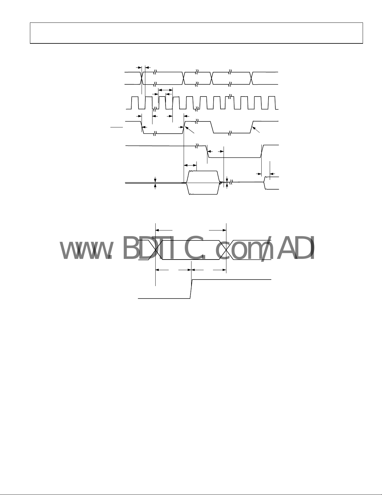
Figure 3. Serial Interface Timing
VALID DATA BIT
DAT
CLK
MSB-1MSB MSB-2
t
DS
t
DH
Figure 4. SDATA Timing
3158-004
Rev. A | Page 5 of 20

AD8328
www.BDTIC.com/ADI
ABSOLUTE MAXIMUM RATINGS
Table 4.
Parameter Rating
Supply Voltage VCC 6 V
Input Voltage
V
, V
1.5 V p-p
IN+
IN−
DATEN, SDATA, CLK, SLEEP, TXEN
Internal Power Dissipation
QSOP (θJA = 83.2°C/W)
LFCSP (θJA = 30.4°C/W)
Operating Temperature Range −40°C to +85°C
Storage Temperature Range −65°C to +150°C
Lead Temperature, Soldering 60 sec 300°C
1
Thermal resistance measured on SEMI standard 4-layer board.
2
Thermal resistance measured on SEMI standard 4-layer board, paddle
soldered to board.
1
2
−0.8 V to +5.5 V
700 mW
700 mW
Stresses above those listed under Absolute Maximum Ratings
may cause permanent damage to the device. This is a stress
rating only; functional operation of the device at these or any
other conditions above those indicated in the operational
section of this specification is not implied. Exposure to absolute
maximum rating conditions for extended periods may affect
device reliability.
ESD CAUTION
ESD (electrostatic discharge) sensitive device. Electrostatic charges as high as 4000 V readily accumulate on
the human body and test equipment and can discharge without detection. Although this product features
proprietary ESD protection circuitry, permanent damage may occur on devices subjected to high energy
electrostatic discharges. Therefore, proper ESD precautions are recommended to avoid performance
degradation or loss of functionality.
Rev. A | Page 6 of 20
 Loading...