Analog Devices AD8326 Datasheet
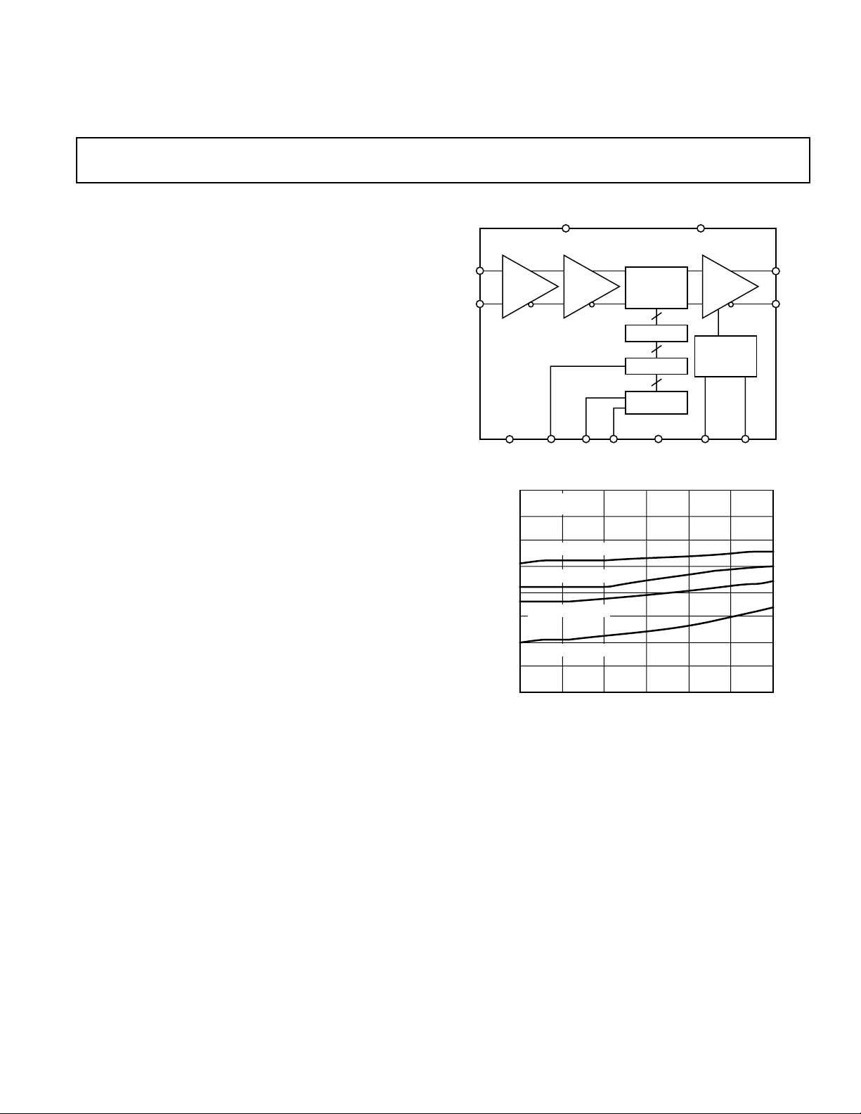
High Output Power
–40
–45
–50
–55
–60
–65
–70
–75
–80
5 15 25 35 45 55 65
DISTORTION – dBc
FREQUENCY – MHz
ARP(VS = +12V)
ARE(VS = ⴞ5V)
ARP(VO = 69dBmV)
ARP(VO = 67dBmV)
ARE(VO = 65dBmV)
ARE(VO = 62dBmV)
a
FEATURES
Supports DOCSIS Standard for Reverse Path
Transmission
Gain Programmable in 0.75 dB Steps over a 53.5 dB Range
Low Distortion at 65 dBmV Output
–62 dBc SFDR at 21 MHz
–58 dBc SFDR at 65 MHz
1 dB Compression of 25 dBm at 10 MHz
Output Noise Level
–45 dBmV in 160 kHz
Maintains 75 ⍀ Output Impedance
Power-Up and Power-Down Condition
Upper Bandwidth: 100 MHz (Full Gain Range)
Single or Dual Supply Operation
APPLICATIONS
Gain-Programmable Line Driver
CATV Telephony Modems
CATV Terminal Devices
General-Purpose Digitally Controlled Variable Gain Block
Programmable CATV Line Driver
AD8326
FUNCTIONAL BLOCK DIAGRAM
V
IN+
V
IN–
ZIN (SINGLE) = 800⍀
Z
(DIFF) = 1.6k⍀
IN
DIFF OR
SINGLE
INPUT
AMP
GND
VCC (7 PINS)
VERNIER
DATEN
AD8326
DATA CLK V
ATTENUATION
CORE
DECODE
DATA LATCH
SHIFT
REGISTER
(10 PINS)
EE
8
8
8
BYP
POWER
AMP
Z
OUT
POWER-DOWN
LOGIC
TXEN
SLEEP
DIFF =
75⍀
V
V
OUT+
OUT–
GENERAL DESCRIPTION
The AD8326 is a high-output power, digitally controlled, variable gain amplifier optimized for coaxial line driving applications
such as data and telephony cable modems that are designed to
the MCNS-DOCSIS upstream standard. An 8-bit serial word
determines the desired output gain over a 53.5 dB range resulting in gain changes of 0.75 dB/LSB. The AD8326 is offered in
two models, each optimized to support the desired output power
and resulting performance.
The AD8326 comprises a digitally controlled variable attenuator
of 0 dB to –54 dB, that is preceded by a low noise, fixed-gain
buffer and is followed by a low distortion high-power amplifier.
The AD8326 accepts a differential or single-ended input signal.
The output is designed to drive a 75 Ω load, such as coaxial
cable, although the AD8326 is capable of driving other loads.
When driving 67 dBm into a 75 Ω load, the AD8326ARP
provides a worst harmonic of only –59 dBc at 21 MHz and
–57 dBc at 42 MHz. When driving 65 dBmV into a 75 Ω load,
the AD8326ARE provides a worst harmonic of only –62 dBc at
21 MHz and –60 dBc at 42 MHz.
REV. 0
Information furnished by Analog Devices is believed to be accurate and
reliable. However, no responsibility is assumed by Analog Devices for its
use, nor for any infringements of patents or other rights of third parties that
may result from its use. No license is granted by implication or otherwise
under any patent or patent rights of Analog Devices.
Figure 1. Worst Harmonic Distortion vs. Frequency
The differential output of the AD8326 is compliant with DOCSIS
paragraph 4.2.10.2 for “Spurious Emissions During Burst On/Off
Transients.” In addition, this device has a sleep mode function
that reduces the quiescent current to 4 mA.
The AD8326 is packaged in a low-cost 28-lead TSSOP and a
28-lead P (power) SOIC. Both devices have an operational tem-
perature range of –40°C to +85°C.
One Technology Way, P.O. Box 9106, Norwood, MA 02062-9106, U.S.A.
Tel: 781/329-4700 www.analog.com
Fax: 781/326-8703 © Analog Devices, Inc., 2001

AD8326–SPECIFICA TIONS
(TA = 25ⴗC, VS = 12 V, RL = RIN = 75 ⍀, VIN = 259 mV p-p, V
transformer with an insertion loss of 0.5 dB @ 10 MHz, unless otherwise noted.)
measured through a 1:1
OUT
AD8326ARP
Parameter Conditions Min Typ Max Unit
INPUT CHARACTERISTICS
Specified AC Voltage Output = 67 dBmV, Max Gain 259 mV p-p
Noise Figure Max Gain, f = 10 MHz 16.6 dB
Input Resistance Differential Input 1600 Ω
Single-Ended Input 800 Ω
Input Capacitance 2pF
GAIN CONTROL INTERFACE
Gain Range 52.5 53.5 54.5 dB
Maximum Gain Gain Code = 71 Dec 26.5 27.5 28.5 dB
Minimum Gain Gain Code = 0 Dec –27 –26 –25 dB
Gain Scaling Factor 0.7526 dB/LSB
Gain Linearity Error f = 10 MHz, Code-to-Code ±0.2 dB
OUTPUT CHARACTERISTICS
Bandwidth (–3 dB) All Gain Codes 100 MHz
Bandwidth Roll-Off f = 65 MHz 1.2 dB
Bandwidth Peaking f = 65 MHz 0 dB
Output Noise Spectral Density Max Gain, f = 10 MHz –28 dBmV in
160 kHz
Min Gain, f = 10 MHz –45.5 dBmV in
160 kHz
Transmit Disable Mode, f = 10 MHz –65 dBmV in
160 kHz
1 dB Compression Point Max Gain, f = 10 MHz 26.5 dBm
Differential Output Impedance Transmit Enable and Transmit Disable Mode 75 ± 20% Ω
OVERALL PERFORMANCE
Worst Harmonic Distortion f = 14 MHz, V
f = 21 MHz, V
f = 42 MHz, V
f = 65 MHz, V
Adjacent Channel Power 16 QAM, V
= 67 dBmV @ Max Gain –59 dBc
OUT
= 67 dBmV @ Max Gain –59 dBc
OUT
= 67 dBmV @ Max Gain –57 dBc
OUT
= 67 dBmV @ Max Gain –55 dBc
OUT
= 67 dBmV –56 dBc
OUT
Adj Ch Wid = Tr Ch Wid = 160 KSYM/SEC
Output Settling
Due to Gain Change (T
Due to Input Step Change Max Gain, V
Signal Isolation Min Gain, TXEN = 0, 65 MHz, V
) Min to Max Gain 60 ns
GS
Max Gain, TXEN = 0, 42 MHz, V
Max Gain, TXEN = 0, 65 MHz, V
= 0 V to 0.25 V p-p 30 ns
IN
= 0.25 V p-p –85 dBc
IN
= 0.25 V p-p –31 dBc
IN
= 0.25 V p-p –28 dBc
IN
All Gains, SLEEP, 65 MHz, VIN = 0.25 V p-p –85 dBc
POWER CONTROL
Transmit Enable Response Time (t
Transmit Disable Response Time (t
Between Burst Transients
1
) Max Gain, VIN = 0 250 ns
ON
) Max Gain, VIN = 0 40 ns
OFF
Equivalent Output = 31 dBmV 5 mV p-p
Equivalent Output = 61 dBmV 60 mV p-p
POWER SUPPLY
Operating Range 11.4 12 12.6 V
Quiescent Current Transmit Enable Mode (TXEN = 1) 147 157 167 mA
Transmit Disable Mode (TXEN = 0) 38 44 50 mA
Sleep Mode 1.5 4.5 7.5 mA
OPERATING TEMPERATURE –40 +85 °C
RANGE
NOTES
1
Between Burst Transients measured at the output of diplexer.
Specifications subject to change without notice.
–2–
REV. 0

AD8326
SPECIFICA TIONS
(TA = 25ⴗC, VS = ⴞ5 V, RL = RIN = 75 ⍀, VIN = 206 V p-p, V
transformer with an insertion loss of 0.5 dB @ 10 MHz, unless otherwise noted.)
measured through a 1:1
OUT
AD8326ARE
Parameter Conditions Min Typ Max Unit
INPUT CHARACTERISTICS
Specified AC Voltage Output = 65 dBmV, Max Gain 206 mV p-p
Noise Figure Max Gain, f = 10 MHz 16.6 dB
Input Resistance Differential Input 1600 Ω
Single-Ended Input 800 Ω
Input Capacitance 2pF
GAIN CONTROL INTERFACE
Gain Range 52.5 53.5 54.5 dB
Maximum Gain Gain Code = 71 Dec 26.5 27.5 28.5 dB
Minimum Gain Gain Code = 0 Dec –27 –26 –25 dB
Gain Scaling Factor 0.7526 dB/LSB
Gain Linearity Error f = 10 MHz, Code-to-Code ±0.2 dB
OUTPUT CHARACTERISTICS
Bandwidth (–3 dB) All Gain Codes 100 MHz
Bandwidth Roll-Off f = 65 MHz 1.1 dB
Bandwidth Peaking f = 65 MHz 0 dB
Output Noise Spectral Density Max Gain, f = 10 MHz –28 dBmV in
160 kHz
Min Gain, f = 10 MHz –45.5 dBmV in
160 kHz
Transmit Disable Mode, f = 10 MHz –65 dBmV in
160 kHz
1 dB Compression Point Max Gain, f = 10 MHz 25.0 dBm
Differential Output Impedance Transmit Enable and Transmit Disable Mode 75 ± 20% Ω
OVERALL PERFORMANCE
Worst Harmonic Distortion f = 14 MHz, V
f = 21 MHz, V
f = 42 MHz, V
f = 65 MHz, V
Adjacent Channel Power 16 QAM, V
= 65 dBmV @ Max Gain –62 dBc
OUT
= 65 dBmV @ Max Gain –62 dBc
OUT
= 65 dBmV @ Max Gain –60 dBc
OUT
= 65 dBmV @ Max Gain –58 dBc
OUT
= 65 dBmV –58 dBc
OUT
Adj Ch Wid = Tr Ch Wid = 160 KSYM/SEC
Output Settling
Due to Gain Change (T
Due to Input Step Change Max Gain, V
Signal Isolation Min Gain, TXEN = 0, 65 MHz, V
) Min to Max Gain 60 ns
GS
Max Gain, TXEN = 0, 42 MHz, V
Max Gain, TXEN = 0, 65 MHz, V
= 0 V to 0.19 V p-p 30 ns
IN
= 0.19 V p-p –85 dBc
IN
= 0.19 V p-p –31 dBc
IN
= 0.19 V p-p –28 dBc
IN
All Gains, SLEEP, 65 MHz, VIN = 0.19 V p-p –85 dBc
POWER CONTROL
Transmit Enable Response Time (tON) Max Gain, VIN = 0 250 ns
Transmit Disable Response Time (t
Between Burst Transients
1
) Max Gain, VIN = 0 40 ns
OFF
Equivalent Output = 31 dBmV 5 mV p-p
Equivalent Output = 61 dBmV 60 mV p-p
POWER SUPPLY
Operating Range ±4.75 ±5.0 ±5.25 V
Quiescent Current Transmit Enable Mode (TXEN = 1) 140 150 160 mA
Transmit Disable Mode (TXEN = 0) 36 42 48 mA
Sleep Mode 1 4 7 mA
OPERATING TEMPERATURE –40 +85 °C
RANGE
NOTES
1
Between Burst Transients measured at the output of diplexer.
Specifications subject to change without notice.
REV. 0
–3–
AD8326
LOGIC INPUTS (TTL/CMOS Compatible Logic)
(DATEN, CLK, SDATA, TXEN, SLEEP, V
= 12 V: Full Temperature Range)
CC
Parameter Min Typ Max Unit
Logic “1” Voltage 2.1 5.0 V
Logic “0” Voltage 0 0.8 V
Logic “1” Current (V
Logic “0” Current (V
Logic “1” Current (V
Logic “0” Current (V
Logic “1” Current (V
Logic “0” Current (V
Specifications subject to change without notice.
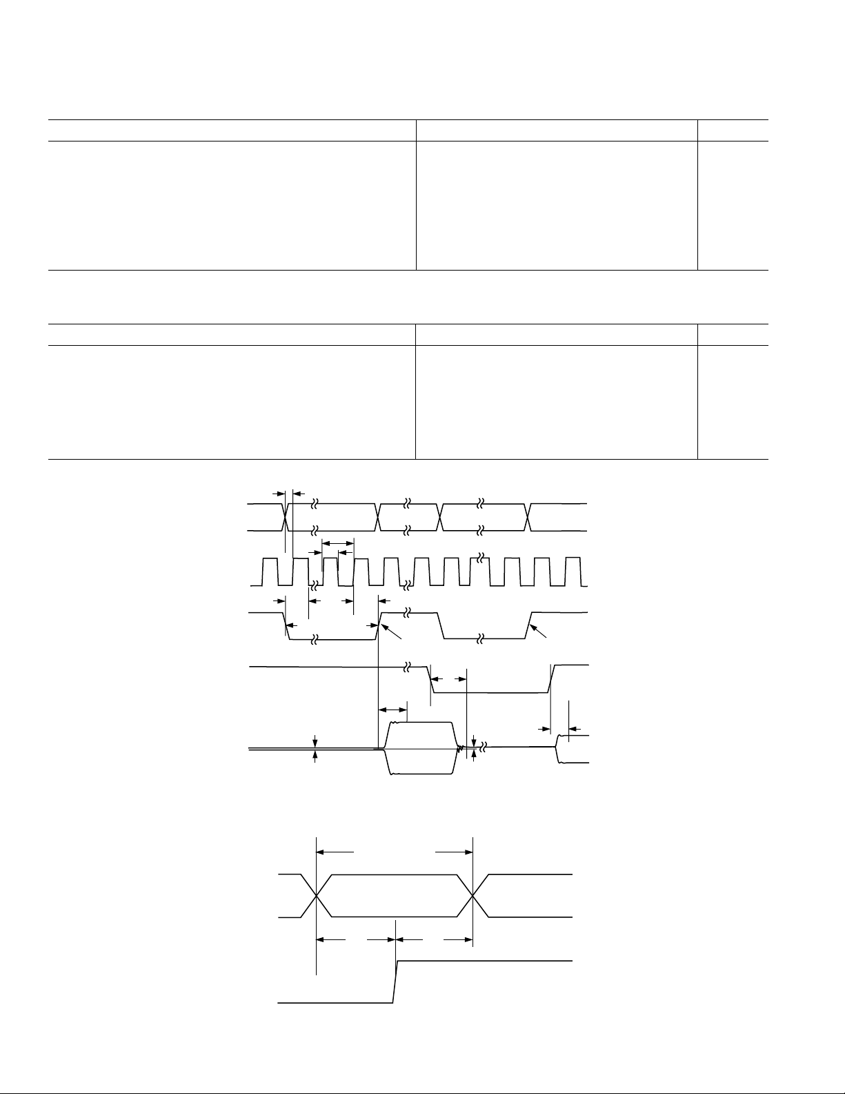
TIMING REQUIREMENTS
= 5 V) CLK, SDATA, DATEN 020nA
INH
= 0 V) CLK, SDATA, DATEN –600 –100 nA
INL
= 5 V) TXEN 50 190 µA
INH
= 0 V) TXEN –250 –30 µA
INL
= 5 V) SLEEP 50 190 µA
INH
= 0 V) SLEEP –250 –30 µA
INL
(Full Temperature Range, VCC = 12 V, tR = tF = 4 ns, f
= 8 MHz unless otherwise noted.)
CLK
Parameter Min Typ Max Unit
Clock Pulsewidth (t
Clock Period (t
Setup Time SDATA vs. Clock (t
Setup Time DATEN vs. Clock (t
Hold Time SDATA vs. Clock (t
Hold Time DATEN vs. Clock (t
) 16.0 ns
WH
) 32.0 ns
C
) 5.0 ns
DS
) 15.0 ns
ES
) 5.0 ns
DH
) 3.0 ns
EH
Input Rise and Fall Times, SDATA, DATEN, Clock (tR, tF)10ns
Specifications subject to change without notice.
t
DS
SDATA
CLK
VALID DATA WORD G1
MSB. . . .LSB
t
C
t
WH
VALID DATA WORD G2
DATEN
TXEN
ANALOG
OUTPUT
t
ES
8 CLOCK CYCLES
SIGNAL AMPLITUDE (p-p)
Figure 2. Serial Interface Timing
SDATA
MSB
CLK
t
EH
GAIN TRANSFER (G1)
t
GS
VALID DATA BIT
MSB-1 MSB-2
t
DS
GAIN TRANSFER (G2)
t
OFF
t
ON
t
DH
Figure 3. SDATA Timing
–4–
REV. 0
ABSOLUTE MAXIMUM RATINGS*
Supply Voltage V
CC
Pins 5, 9, 10, 19, 20, 23, 27 . For ARP, Max VCC = VEE + 13 V;
. . . . . . . . . . . . . . . . . . . . . . . For ARE, Max V
= VEE + 11 V
CC
Input Voltages
Pins 25, 26 . . . . . . . . . . . . . . . . . . . . . . . . . . . . . . . . ±0.5 V
Pins 1, 2, 3, 6, 7 . . . . . . . . . . . . . . . . . . . . . –0.8 V to +5.5 V
Internal Power Dissipation
TSSOP EPAD . . . . . . . . . . . . . . . . . . . . . . . . . . . . . . 1.5 W
PSOP . . . . . . . . . . . . . . . . . . . . . . . . . . . . . . . . . . . . . .2.0 W
Operating Temperature Range . . . . . . . . . . . –40°C to +85°C
Storage Temperature Range . . . . . . . . . . . . –65°C to +150°C
Lead Temperature, Soldering 60 seconds . . . . . . . . . . . 300°C
*Stresses above those listed under Absolute Maximum Ratings may cause perma-
nent damage to the device. This is a stress rating only; functional operation of the
device at these or any other conditions above those indicated in the operational
section of this specification is not implied. Exposure to absolute maximum rating
conditions for extended periods may affect device reliability.
ORDERING GUIDE
AD8326
Model Temperature Range Package Description
JA
Package Option
AD8326ARP –40°C to +85°C 28-Lead Power SOIC with Slug 23°C/W* RP-28
AD8326ARP-REEL
AD8326ARP-EVAL Evaluation Board
AD8326ARE –40°C to +85°C 28-Lead TSSOP with Exposed Pad 39°C/W* RE-28
AD8326ARE-REEL
AD8326ARE-EVAL Evaluation Board
*Thermal Resistance measured on SEMI standard 4-layer board.
CAUTION
ESD (electrostatic discharge) sensitive device. Electrostatic charges as high as 4000 V readily
accumulate on the human body and test equipment and can discharge without detection. Although
the AD8326 features proprietary ESD protection circuitry, permanent damage may occur on
devices subjected to high-energy electrostatic discharges. Therefore, proper ESD precautions are
recommended to avoid performance degradation or loss of functionality.
WARNING!
ESD SENSITIVE DEVICE
REV. 0
–5–
AD8326
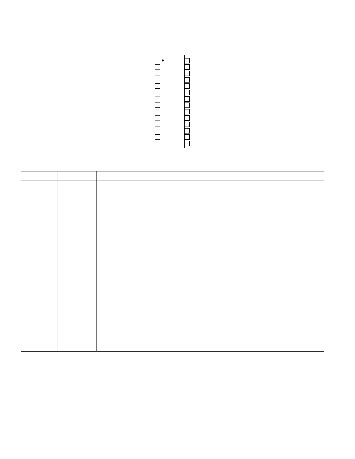
PIN CONFIGURATION
1
DATEN
2
SDATA V
3
CLK V
4
GND V
5
V
CC
6
TXEN
SLEEP
OUT– OUT+
AD8326
7
TOP VIEW
(Not to Scale)
8
NC BYP
9
V
CC
10
V
CC
11
V
EE
12
NC NC
13
V
EE
14
NC = NO CONNECT
GND
28
27
CC
26
IN–
25
IN+
V
24
EE
V
23
CC
V
22
EE
21
V
20
CC
V
19
CC
V
18
EE
17
V
16
EE
15
PIN FUNCTION DESCRIPTIONS
Pin No. Mnemonic Description
1 DATEN Data Enable Low Input. This port controls the 8-bit parallel data latch and shift register. A Logic
0-to-1 transition transfers the latched data to the attenuator core (updates the gain) and simultaneously inhibits serial data transfer into the register. A 1-to-0 transition inhibits the data latch
(holds the previous gain state) and simultaneously enables the register for serial data load.
2 SDATA Serial Data Input. This digital input allows for an 8-bit serial (gain) word to be loaded into the
internal register with the MSB (Most Significant Bit) first and ignored.
3 CLK Clock Input. The clock port controls the serial attenuator data transfer rate to the 8-bit master-
slave register. A Logic 0-to-1 transition latches the data bit and a 1-to-0 transfers the data bit to
the slave. This requires the input serial data word to be valid at or before this clock transition.
4, 28 GND Common External Ground Reference
5, 9, 10, 19, V
CC
Common Positive External Supply Voltage. A 0.1 µF capacitor must decouple each pin.
20, 23, 27
6 TXEN Transmit Enable pin. Logic 1 powers up the part.
7 SLEEP Low Power Sleep Mode. In the Sleep mode, the AD8326’s supply current is reduced to 4 mA. A
Logic 0 powers down the part (High Z
State) and a Logic 1 powers up the part.
OUT
8, 12, 17 NC No Connection to these pins.
11, 13, 16, 18, V
EE
Common Negative External Supply Voltage. A 0.1 µF capacitor must decouple each pin.
22, 24
14 OUT– Negative Output Signal
15 OUT+ Positive Output Signal
21 BYP Internal Bypass. This pin must be externally ac-coupled (0.1 µF capacitor).
25 V
IN+
Noninverting Input. DC-biased to approximately VCC/2. Should be ac-coupled with a
0.1 µF capacitor.
26 V
IN–
Inverting Input. DC-biased to approximately V
CC
/2. Should be ac-coupled with a 0.1 µF capacitor.
–6–
REV. 0
+1/2 V
–26
–30
–34
–38
–42
–46
–50
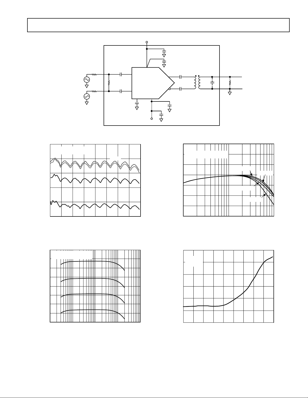
GAIN CONTROL – Decimal
OUTPUT NOISE – dBmV in 160 kHz
0 8 16 24 32 40 48 56 64 72
f = 10MHz
TXEN = 1
V
S
= 12V
–1/2 V
Typical Performance Characteristics–
V
CC
10F
0.1F
75⍀
IN
75⍀
IN
0.1F
165⍀
0.1F
0.1F
V
V
BYP
IN+
IN–
V
CC
AD8326
V
EE
V
EE
OUT+
OUT–
10F
0.1F
0.1F
0.1F
1:1
TOKO
617DB-A0070
C
L
75⍀
+
V
–
AD8326
O
TPC 1. Test Circuit
1.0
VS = 12V
= 67dBmV@ MAX GAIN
P
O
0.5
0
–0.5
GAIN ERROR – dB
–1.0
–1.5
0 9 18 27 36 45 54 63 72
GAIN CONTROL – Decimal
10MHz
5MHz
42MHz
65MHz
TPC 2. Gain Error vs. Gain Control
40
VS = 12V
= 67dBmV @ MAX GAIN
V
O
30
20
10
0
GAIN – dB
–10
–20
–30
–40
0.1 1 10 100 1000
FREQUENCY – MHz
71D
46D
23D
00D
TPC 3. AC Response
32.0
VS = 12V
GAIN – dB
30.5
29.0
27.5
26.0
24.5
23.0
21.5
= 67dBmV @ MAX GAIN
P
OUT
1
10
FREQUENCY – MHz
CL = 0pF
CL = 10pF
CL = 20pF
CL = 50pF
100
TPC 4. AC Response for Various Capacitor Loads
TPC 5. Output Referred Noise vs. Gain Control
REV. 0
–7–
AD8326
–50
VS = 12V
–55
f
= 42MHz
P
= 67dBmV @ MAX GAIN
O
–60
–65
–70
–75
DISTORTION – dBc
–80
–85
–90
0 9 18 27 36 45 54 63 72
GAIN CODE – Decimal
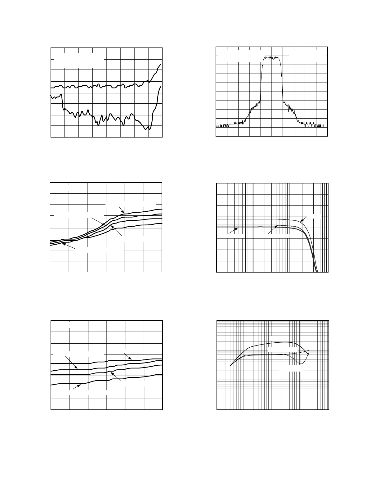
HD3
HD2
TPC 6. Harmonic Distortion vs. Gain Code for
AD8326-ARP
–50
VS = 12V(ARP)
–55
–60
VO = 68dBmV @ MAX GAIN
–65
–70
–75
DISTORTION – dBc
–80
–85
–90
5 15 25 35 45 55 65
VO = 65dBmV @ MAX GAIN
FREQUENCY – MHz
VO = 69dBmV @ MAX GAIN
VO = 67dBmV @ MAX GAIN
0
RBW 500Hz RF ATT 30dB
–10
VBW 5kHz
SWT 20s UNIT dBm
–20
–30
–40
–50
–60
–70
–80
–90
–100
CENTER 21MHz 100kHz/ SPAN 1MHz
CH PWR +12.27dBm
ACP UP –56.72dB
ACP LOW –56.71dB
TPC 9. Adjacent Channel Power for AD8326-ARP
190
180
170
160
150
IMPEDANCE – ⍀
140
130
120
110
1 10 100 1000
POWER-DOWNPOWER-UP
FREQUENCY – MHz
SLEEP
TPC 7. Second Order Harmonic Distortion vs. Frequency
for Various Output Powers
–35
VS = +12V(ARP)
–40
–45
VO = 68dBmV @ MAX GAIN
–50
–55
–60
DISTORTION – dBc
–65
VO = 65dBmV @ MAX GAIN
–70
–75
5 15 25 35 45 55 65
FREQUENCY – MHz
VO = 69dBmV @ MAX GAIN
VO = 67dBmV @ MAX GAIN
TPC 8. Third Order Harmonic Distortion vs. Frequency
for Various Output Powers
TPC 10. Input Impedance vs. Frequency (Inputs
Ω
Shunted with 165
1000
100
10
IMPEDANCE – ⍀
1
0.1 1 10 100 1000
)
SLEEP
POWER-DOWN
POWER-UP
FREQUENCY – MHz
TPC 11. Output Impedance vs. Frequency
–8–
REV. 0
 Loading...