ANALOG DEVICES AD8322 Service Manual

CAT-5 Receiver with
FEATURES
Tuned to compensate for Category-5 (CAT-5) cable losses
Up to 100 meters @ 120 MHz
2 voltage-controlled frequency response adjustment pins
High frequency peaking adjustment
Broadband gain adjustment
2700 V/μs slew rate
Low output noise
1.5 mV rms integrated noise (1 GHz) @ 100 meters
equalized bandwidth
DC output offset adjust
Low offset voltage error: 7 mV typ
Equalized pass-band ripple ±1 dB to 70 MHz
Input: differential or single ended
Supply current: 24 mA on ±5 V
Small 8-lead 3 mm × 3 mm LFCSP
APPLICATIONS
Keyboard-video-mouse (KVM)
RGB video over unshielded twisted pair (UTP) cable receivers
Professional video projection and distribution
Security video
Adjustable Line Equalization
AD8128
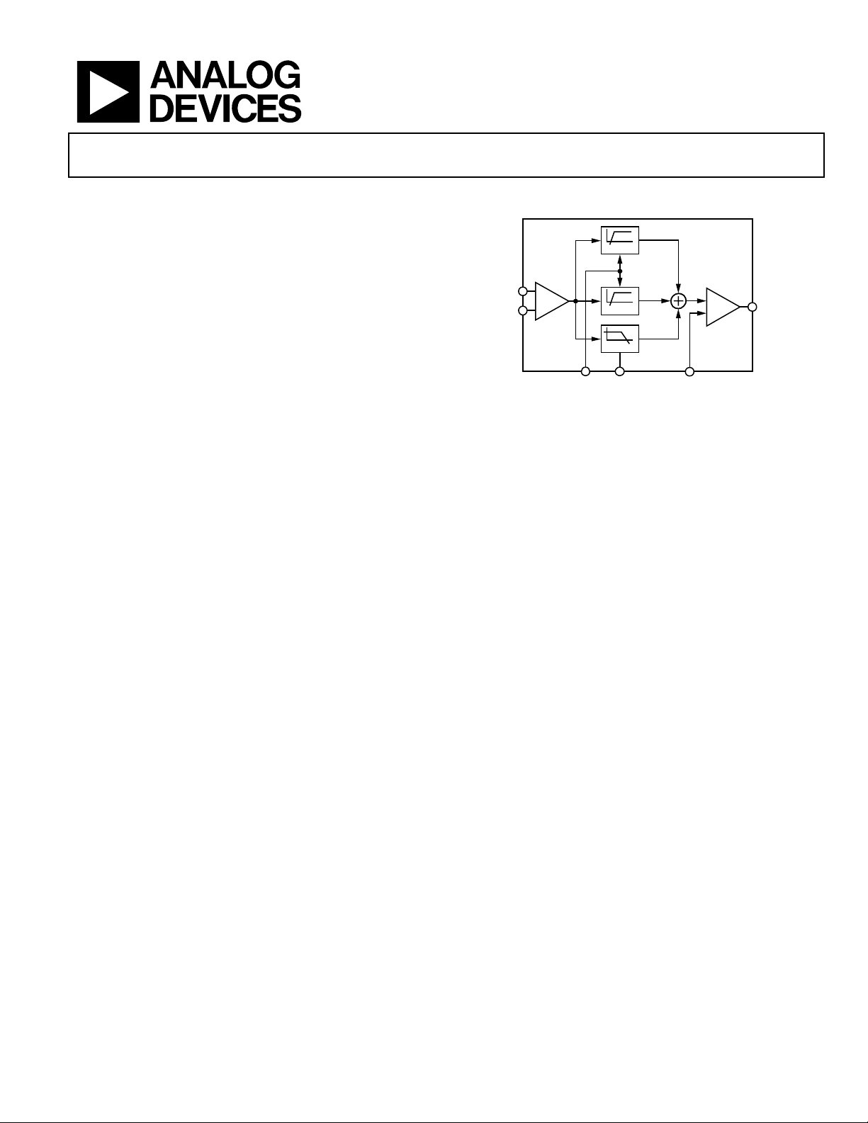
FUNCTIONAL BLOCK DIAGRAM
V
OFFSET
AD8128
V
OUT
05699-001
HPF
V
IN+
V
PEAK
V
HPF
LPF
GAIN
Figure 1.
V
IN–
GENERAL DESCRIPTION
The AD8128 is a high speed, differential receiver/equalizer that
compensates for the transmission losses of unshielded twisted
pair (UTP) CAT-5 cables. Various frequency dependent gain
stages are summed together to best approximate the inverse
frequency response of CAT-5/CAT-5e cable. An equalized
bandwidth of 120 MHz can be achieved for 100 meters of cable.
The AD8128 can be used as a standalone receiver/equalizer or
in conjunction with the AD8143, triple differential receiver, to
provide a complete low cost solution for receiving RGB over
UTP cable in such applications as KVM.
The AD8128 has three control pins for optimal CAT-5/CAT-5e
compensation. The equalized cable length is directly proportional
to the voltage applied to the V
amount of high frequency peaking. V
gain from 0 dB to 3 dB, compensating for the resistive cable
loss. V
allows the output to be shifted by ±2.5 V, adding
OFFSET
flexibility for dc-coupled systems.
Rev. 0
Information furnished by Analog Devices is believed to be accurate and reliable. However, no
responsibility is assumed by Anal og Devices for its use, nor for any infringements of patents or ot her
rights of third parties that may result from its use. Specifications subject to change without notice. No
license is granted by implication or otherwise under any patent or patent rights of Analog Devices.
Trademarks and registered trademarks are the property of their respective owners.
pin, which controls the
PEAK
adjusts the broadband
GAIN
Low integrated output noise and offset voltage adjust make the
AD8128 an excellent choice for dc-coupled wideband RGBover-CAT-5 applications. For systems where the UTP cable is
longer than 100 meters, two AD8128s can be cascaded to
compensate for up to 200 meters of CAT-5/CAT-5e.
The AD8128 is available in a 3 mm × 3 mm 8-lead LFCSP and
is rated to operate over the extended temperature range of
−40°C to +85°C.
One Technology Way, P.O. Box 9106, Norwood, MA 02062-9106, U.S.A.
Tel: 781.329.4700 www.analog.com
Fax: 781.461.3113 © 2005 Analog Devices, Inc. All rights reserved.

AD8128
TABLE OF CONTENTS
Features .............................................................................................. 1
Theory of Operation .........................................................................9
Applications....................................................................................... 1
Functional Block Diagram .............................................................. 1
General Description......................................................................... 1
Revision History ............................................................................... 2
Specifications..................................................................................... 3
Absolute Maximum Ratings............................................................ 4
Thermal Resistance ...................................................................... 4
ESD Caution.................................................................................. 4
Pin Configuration and Function Descriptions............................. 5
Typical Performance Characteristics ............................................. 6
Test Cir c ui t .................................................................................... 8
REVISION HISTORY
10/05—Revision 0: Initial Version
Input Common-Mode Voltage Range Considerations ............9
Applications..................................................................................... 10
KVM Applications ..................................................................... 10
DC Control Pins......................................................................... 10
Cascaded Applications............................................................... 11
Exposed Pad (EP)....................................................................... 11
Layout and Power Supply Decoupling Considerations......... 11
Evaluation Boards ...................................................................... 11
Outline Dimensions ....................................................................... 12
Ordering Guide .......................................................................... 12
Rev. 0 | Page 2 of 12

AD8128
SPECIFICATIONS
TA = 25°C, VS = ±5 V, RL = 150 Ω, Belden Cable, V
Table 1.
Parameter Conditions Min Typ Max Unit
DYNAMIC PERFORMANCE
–3 dB Large Signal Bandwidth V
±1 dB Equalized Bandwidth Flatness V
Rise/Fall Time V
Rise/Fall Time V
Settling Time to 2% V
Settling Time to 2% V
Integrated Output Voltage Noise V
DC PERFORMANCE
Input Bias Current 15.5 24 μA
V
Pin Current 1.7 8.2 μA
OFFSET
V
Pin Current 2 3.4 μA
GAIN
V
Pin Current 4.2 6.8 μA
PEAK
INPUT CHARACTERISTICS
Input Differential Voltage ±2.8 V
Input Common-Mode Voltage ±3.0 V
Input Resistance Common mode 380 kΩ
Differential 675 kΩ
Input Capacitance 1.7 pF
Common-Mode Rejection Ratio (CMRR) 200 kHz, ΔV
ADJUSTMENT PINS
V
Input Voltage Relative to ground 0 1 V
PEAK
Maximum Peak Gain @ 120 MHz, V
V
Input Relative to ground 0 1 V
GAIN
Maximum Broadband Gain V
V
Input Range Relative to ground ±2.5 V
OFFSET
V
to V
OFFSET
OUT
Gain
OUTPUT CHARACTERISTICS
Output Voltage Swing −2.55 +2.7 V
Output Offset Voltage V
Output Offset Voltage Drift −5.5 μV/°C
Short-Circuit Output Current 100 mA
POWER SUPPLY
Operating Voltage Range ±4.5 ±5.5 V
Quiescent Supply Current, ICC/I
Supply Current Drift, ICC/I
EE
EE
+Power Supply Rejection Ratio (PSRR) RTO −48 −59 dB
−Power Supply Rejection Ratio (PSRR) RTO −48 −61 dB
TEMPERATURE RANGE −40 +85 °C
= 0 V, V
OFFSET
= 2 V p-p, 100 meter CAT-5 120 MHz
OUT
= 2 V p-p 70 MHz
OUT
= 2 V step, 50 meter CAT-5 2 ns
OUT
= 2 V step, 100 meter CAT-5 3.6 ns
OUT
= 2 V step, 50 meter CAT-5 26 ns
OUT
= 2 V step, 100 meter CAT-5 36.4 ns
OUT
= 0.9 V, V
PEAK
= 1 V 3 dB
GAIN
= 0 V, RTO −10.9 +7 +18.7 mV
OFFSET
and V
GAIN
= 225 mV, BW = 1 GHz 1.5 mV rms
GAIN
/ΔV
OUT
IN, cm
= 1 V 20 dB
PEAK
set to optimized settings (see Figure 4), unless otherwise noted.
PEAK
−63 −74 dB
1 V/V
@ ±5 V +24/−21 +31/−27 mA
+86/−77 μA/°C
Rev. 0 | Page 3 of 12

AD8128
A
ABSOLUTE MAXIMUM RATINGS
Table 2.
Parameter Rating
Supply Voltage ±5.5 V
Input Voltage ±V
V
V
PEAK
OFFSET
and V
Control Pins −3 V to +V
GAIN
Control Pins ±V
S
S
S
Operating Temperature Range −40°C to +85°C
Storage Temperature Range −65°C to +125°C
Lead Temperature (Soldering 10 sec) 300°C
Junction Temperature 150°C
Stresses above those listed under Absolute Maximum Ratings
may cause permanent damage to the device. This is a stress
rating only; functional operation of the device at these or any
other conditions above those indicated in the operational
section of this specification is not implied. Exposure to absolute
maximum rating conditions for extended periods may affect
device reliability.
THERMAL RESISTANCE
θJA is specified for the worst-case conditions, that is, a device
soldered in a circuit board for surface-mount packages.
Table 3. Thermal Resistance
Package Type θ
JA
8-Lead LFCSP 77 14 °C/W
Maximum Power Dissipation
θ
JC
Unit
The power dissipated in the package (P
quiescent power dissipation and the power dissipated in the
package due to the load drive for the output. The quiescent
power is the voltage between the supply pins (V
quiescent current (I
drive depends upon the particular application. For each output,
the power due to load drive is calculated by multiplying the load
current by the associated voltage drop across the
Airflow increases heat dissipation, effectively reducing θ
more metal directly in contact with the package leads from
metal traces, through-holes, ground, and power planes reduces
the θ
. The exposed paddle on the underside of the package
JA
must be soldered to a pad on the PCB surface, which is
thermally connected to a copper plane to achieve the specified θ
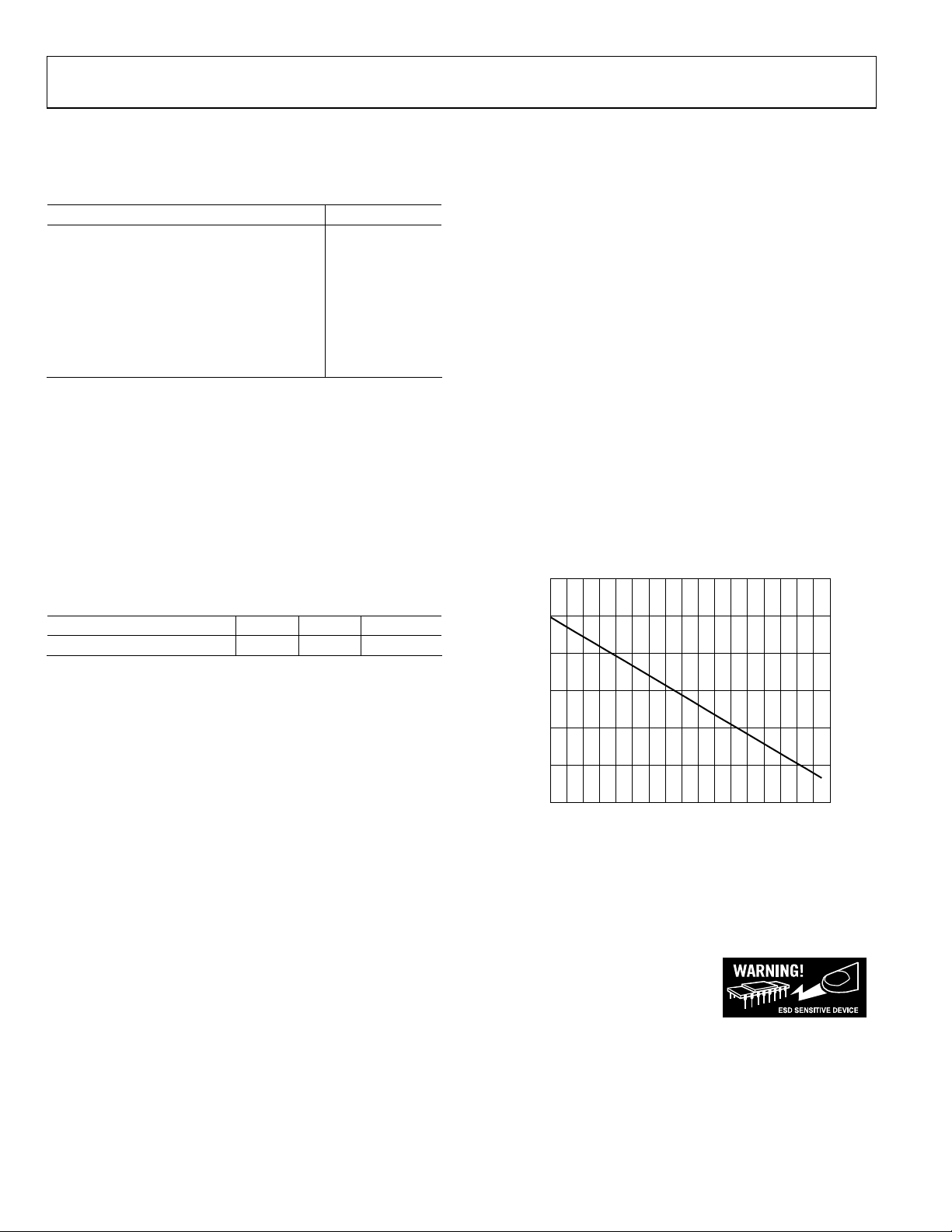
Figure 2 shows the maximum safe power dissipation in the
package vs. the ambient temperature for the 8-lead LFCSP
(48.5°C/W) on a JEDEC standard 4-layer board with the
underside paddle soldered to a pad that is thermally connected
to a PCB plane. Extra thermal relief is required for operation at
high supply voltages.
3.0
2.5
TION (W)
2.0
1.5
The maximum safe power dissipation in the AD8128 package is
limited by the associated rise in junction temperature (T
) on
J
1.0
the die. At approximately 150°C, which is the glass transition
temperature, the plastic changes its properties. Even
0.5
MAXIMUM POWER DISSIP
temporarily exceeding this temperature limit can change the
stresses that the package exerts on the die, permanently shifting
the parametric performance of the AD8128. Exceeding a
junction temperature of 150°C for an extended period can
0
–30–40 –10–20 1003020 5040 7060 9080 110100 130120
Figure 2. Maximum Power Dissipation vs. Temperature
result in changes in the silicon devices potentially causing
failure.
). The power dissipated due to the load
S
AMBIENT T EMPERATURE (°C)
) is the sum of the
D
) times the
S
. Also,
JA
.
JA
05699-020
ESD CAUTION
ESD (electrostatic discharge) sensitive device. Electrostatic charges as high as 4000 V readily accumulate on
the human body and test equipment and can discharge without detection. Although this product features
proprietary ESD protection circuitry, permanent damage may occur on devices subjected to high energy
electrostatic discharges. Therefore, proper ESD precautions are recommended to avoid performance
degradation or loss of functionality.
Rev. 0 | Page 4 of 12
 Loading...