Serial Digital Controlled
a
FEATURES
8-Bit Serial Gain Control
V/V/LSB Linear Gain Response
36 dB Gain Range
60.20 dB Gain Accuracy
Upper Bandwidth: 150 MHz
22 dBm 1 dB Compression Point (75 V)
Drives Low Distortion Signals into 75 V Load:
–57 dBc SFDR at 42 MHz and 12 dBm Out
–46 dBc SFDR at 42 MHz and 18 dBm Out
Single Supply Operation from 5 V to 12 V
Maintains 75 V Output Impedance
Power-Up and Power-Down Condition
Supports SPI Input Control Standard
APPLICATIONS
Coaxial Cable Driver
HFC Cable Telephony Systems
HFC High Speed Data Modems
Interactive Set-Top Boxes
PC Plug-In Modems
Interfaces with AD9853 I
High Performance Digitally Controlled Variable Gain
Block
2
C Controlled Digital Modulator
Variable Gain Line Driver
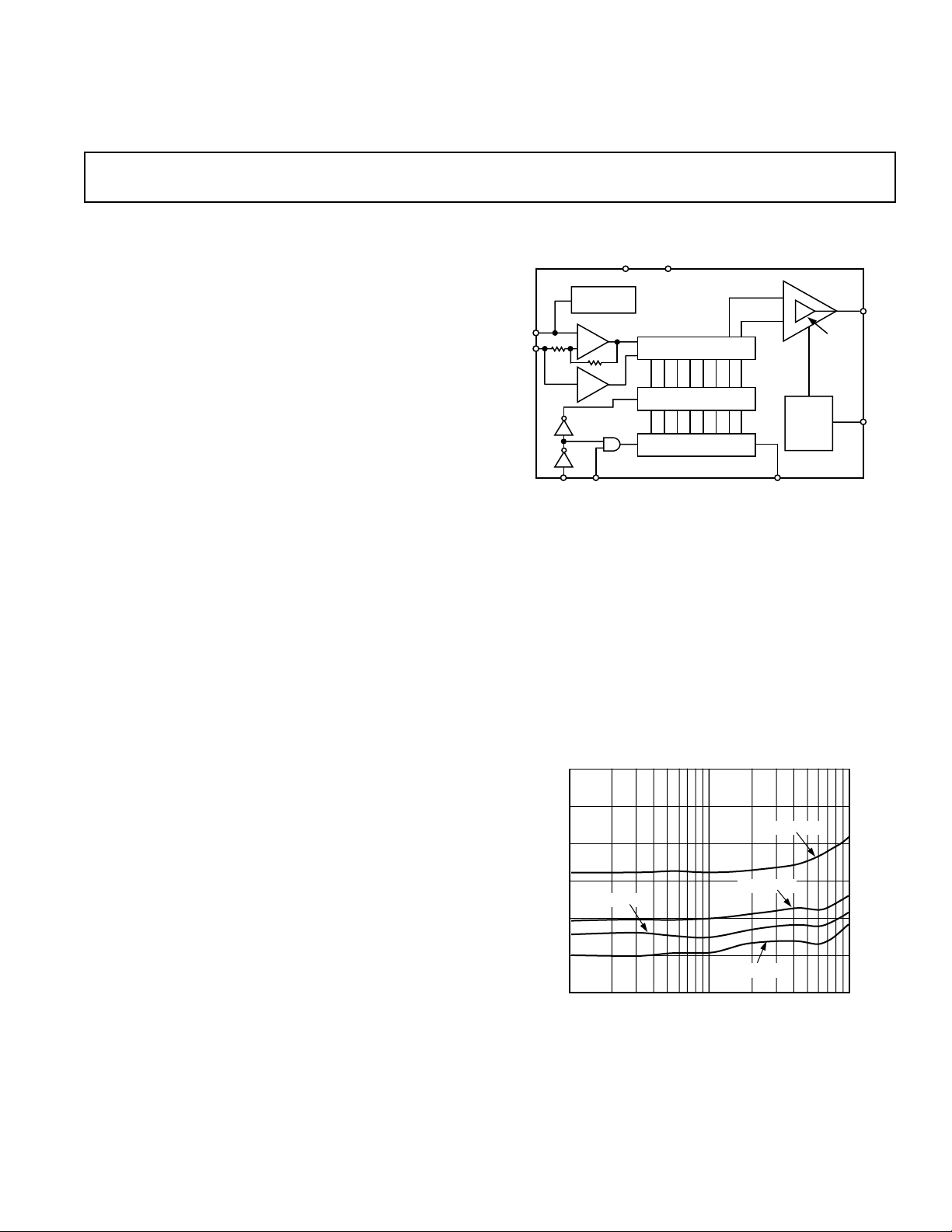
FUNCTIONAL BLOCK DIAGRAM
GNDVCC
REFERENCE
VREF
VIN
INV.
BUF.
DATEN CLK SDATA
AD8320
ATTENUATOR CORE
DATA LATCH
DATA SHIFT REGISTER
AD8320
PWR AMP
REVERSE
AMP
POWER-
DOWN/
SWITCH
INTER.
VOUT
PD
DESCRIPTION
The AD8320 is a digitally controlled variable gain amplifier
optimized for coaxial line driving applications. An 8-bit serial
word determines the desired output gain over a 36 dB range
(256 gain levels). The AD8320 provides linear gain response.
The AD8320 is made up of a digitally controlled variable attenuator of 0 dB to –36 dB, which is preceded by a low noise,
fixed gain buffer and followed by a low distortion high power
amplifier. The AD8320 has a 220 Ω input impedance and accepts a single-ended input signal with a specified analog input
level of up to 0.310 V p-p. The output is specified for driving a
75 Ω load, such as coaxial cable, although the AD8320 is capable of driving other loads. Distortion performance of –57 dBc
is achieved with an output level up to 12 dBm (3.1 V p-p) at
42 M H z, while –46 dBc distortion is achieved with an output
level up to 18 dBm (6.2 V p-p).
A key performance and cost advantage of the AD8320 results
from the ability to maintain a constant 75 Ω output impedance
during power-up and power-down conditions. This eliminates
the need for external 75 Ω back-termination, resulting in twice
the effective output voltage when compared to a standard operational amplifier. Additionally, the on-chip 75Ω termination
REV. 0
Information furnished by Analog Devices is believed to be accurate and
reliable. However, no responsibility is assumed by Analog Devices for its
use, nor for any infringements of patents or other rights of third parties
which may result from its use. No license is granted by implication or
otherwise under any patent or patent rights of Analog Devices.
results in low glitch output during power-down and power-up
transitions, eliminating the need for an external switch.
The AD8320 is packaged in a 20-lead SOIC and operates from
a single +5 V through +12 V supply and has an operational
temperature range of –40°C to +85°C.
220
230
PO = 18dBm
240
250
PO = 8dBm
260
DISTORTION – dBc
270
280
1
FREQUENCY – MHz
PO = 12dBm
PO = 4dBm
10 100
Figure 1. Worst Harmonic Distortion vs. Frequency for
Various Output Levels at V
One Technology Way, P.O. Box 9106, Norwood, MA 02062-9106, U.S.A.
Tel: 781/329-4700 World Wide Web Site: http://www.analog.com
Fax: 781/326-8703 © Analog Devices, Inc., 1998
= 12 V
CC

(@ VCC = 12 V, TA = +258C, VIN = 0.310 V p-p, RL = 75 V, RS = 75 V unless
AD8320–SPECIFICA TIONS
otherwise noted)
Parameter Conditions Min Typ Max Units
INPUT CHARACTERISTICS
Full-Scale Input Voltage Max Gain, P
Max Gain, P
= 18 dBm, VCC = 12 V 0.310 V p-p
OUT
= 12 dBm, VCC = 5 V 0.155 V p-p
OUT
Input Resistance 220 Ω
Input Capacitance 2.0 pF
GAIN CONTROL INTERFACE
Gain Range 36 dB
Full Scale (Max) Gain 26 (20) dB (V/V)
Gain Offset (Min) Gain –10.0 (0.316) dB (V/V)
Gain Scaling Factor 0.077 V/V/LSB
OUTPUT CHARACTERISTICS
Bandwidth (–3 dB) All Gain Codes 150 MHz
Bandwidth Roll-Off F = 65 MHz 0.7 dB
Bandwidth Peaking F = 65 MHz 0 dB
Output Offset Voltage All Gain Codes ± 40 mV
Output Offset Drift Full Temperature Range ±0.25 mV/°C
Output Noise Spectral Density Max. Gain, Frequency = 10 MHz 73 nV/√Hz
Min. Gain, Frequency = 10 MHz 53 nV/√ Hz
PD = 0, Frequency = 10 MHz 4.5 nV/√Hz
1 dB Compression Point V
= 12 V 22.5 dBm
CC
V
= 5 V 16 dBm
CC
Output Impedance Power Up and Power Down 65 75 85 Ω
Overload Recovery Max Gain, VIN = 500 mV p-p 40 ns
OVERALL PERFORMANCE
Worst Harmonic Distortion F = 42 MHz, P
F = 42 MHz, P
F = 42 MHz, P
F = 65 MHz, P
F = 65 MHz, P
F = 65 MHz, P
3rd Order Intercept F = 42 MHz, P
F = 42 MHz, P
F = 65 MHz, P
F = 65 MHz, P
= 12 dBm, VCC = 12 V –57.0 –52.0 dBc
OUT
= 12 dBm, VCC = 5 V –43.0 –39.0 dBc
OUT
= 18 dBm, VCC = 12 V –46.0 –42.0 dBc
OUT
= 12 dBm, VCC = 12 V –57.0 –52.0 dBc
OUT
= 12 dBm, VCC = 5 V –42.5 –39.0 dBc
OUT
= 18 dBm, VCC = 12 V –43.0 –40.0 dBc
OUT
= 18 dBm, VCC = 12 V 34 dBm
OUT
= 12 dBm, VCC = 5 V 32 dBm
OUT
= 18 dBm, VCC = 12 V 32.5 dBm
OUT
= 12 dBm, VCC = 5 V 28.5 dBm
OUT
Full-Scale (Max Gain) Accuracy F = 10 MHz ± 0.1 dB
Gain Offset (Min Gain) Accuracy F = 10 MHz ± 0.2 dB
Gain Accuracy F = 10 MHz, All Gain Codes –0.75 ±0.2 0.75 dB
Gain Drift Full Temperature Range ±0.5 mdB/°C
Gain Variation w/Supply V
= +5 V to 12 V 35 mdB/V
CC
Output Settling to 1 mV
Gain Change @ T
= 1 Min to Max Gain, VIN = 0.31 V p-p 30 ns
DATEN
Input Change Max Gain, VIN = 0 V to 0.31 V p-p 25 ns
POWER CONTROL
Power-Down Settling Time to 1 mV Max Gain, V
Power-Up Settling Time to 1 mV Max Gain, V
Power-Down Pedestal Offset Max Gain, V
= 0 45 ns
IN
= 0 65 ns
IN
= 0 ±30 mV
IN
Spectral Output Leakage F (PD) = 400 Hz @ 15% Duty Cycle –70 dBm
5 MHz ≤ F ≤ 65 MHz
Maximum Reverse Power PD = 0 5 dBm
POWER SUPPLY
Specified Operating Range +5 +12 V
Quiescent Current PD = 1, V
Power Down PD = 0, V
Power Up, V
= +12 V PD = 1, VCC = +12 V 97 105 mA
CC
= +5 V 80 85 mA
CC
= +5 V 25 30 mA
CC
Power Down, VCC =+12 V PD = 0, VCC = +12 V 32 37 mA
–2–
REV. 0
AD8320
LOGIC INPUTS (TTL/CMOS Logic)
(DATEN, CLK, SDATA, 5 V ≤ VCC ≤ 12 V; Full Temperature Range)
Parameter Min Typ Max Units
Logic “1” Voltage 2.1 5.0 V
Logic “0” Voltage 0 0.8 V
Logic “1” Current (V
Logic “0” Current (V
Logic “1” Current (V
Logic “0” Current (V
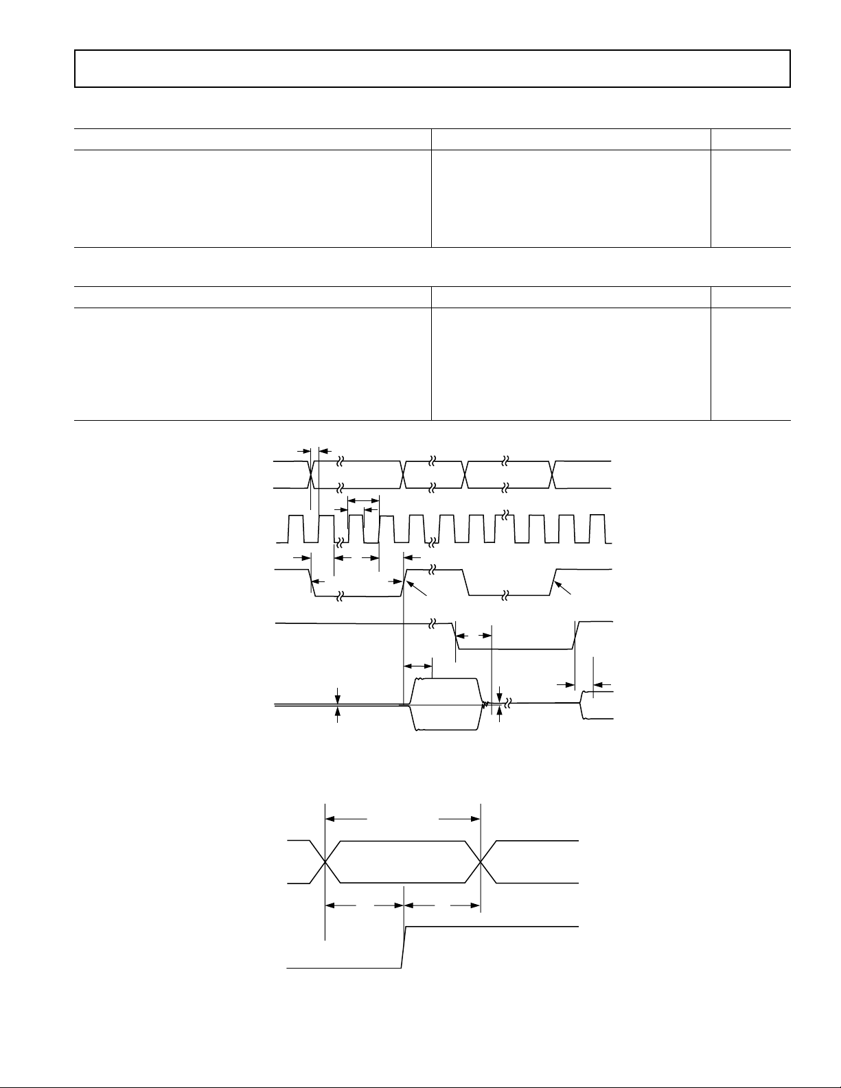
TIMING REQUIREMENTS
= 5 V) CLK, SDATA, DATEN 020nA
INH
= 0 V) CLK, SDATA, DATEN –450 –75 nA
INL
= 5 V) PD 0 190 µA
INH
= 0 V) PD –320 –70 µA
INL
(Full Temperature Range, VCC Supply Range, TR = TF = 4 ns, F
= 8 MHz unless otherwise noted.)
CLK
Parameter Min Typ Max Units
Clock Pulse Width (T
Clock Period (T
C
Setup Time SDATA vs. Clock (T
Setup Time DATEN vs. Clock (T
Hold Time SDATA vs. Clock (T
Hold Time DATEN vs. Clock (T
) 12.0 ns
WH
) 32.0 ns
) 6.5 ns
DS
) 17.0 ns
ES
) 5.0 ns
DH
) 3.0 ns
EH
Input Rise and Fall Times, SDATA, DATEN, Clock (TR, TF)10ns
T
DS
SDATA
CLK
VALID DATA WORD G1
MSB. . . .LSB
T
C
T
WH
VALID DATA WORD G2
DATEN
PD
ANALOG
OUTPUT
T
ES
8 CLOCK CYCLES
SIGNAL AMPLITUDE (p-p)
T
EH
GAIN TRANSFER (G1)
T
Figure 2. Serial Interface Timing
VALID DATA BIT
MSB
T
CLK
MSB-1 MSB-2
DS
GAIN TRANSFER (G2)
T
OFF
GS
T
ON
PEDESTAL
T
DH
Figure 3.
–3–REV. 0
AD8320
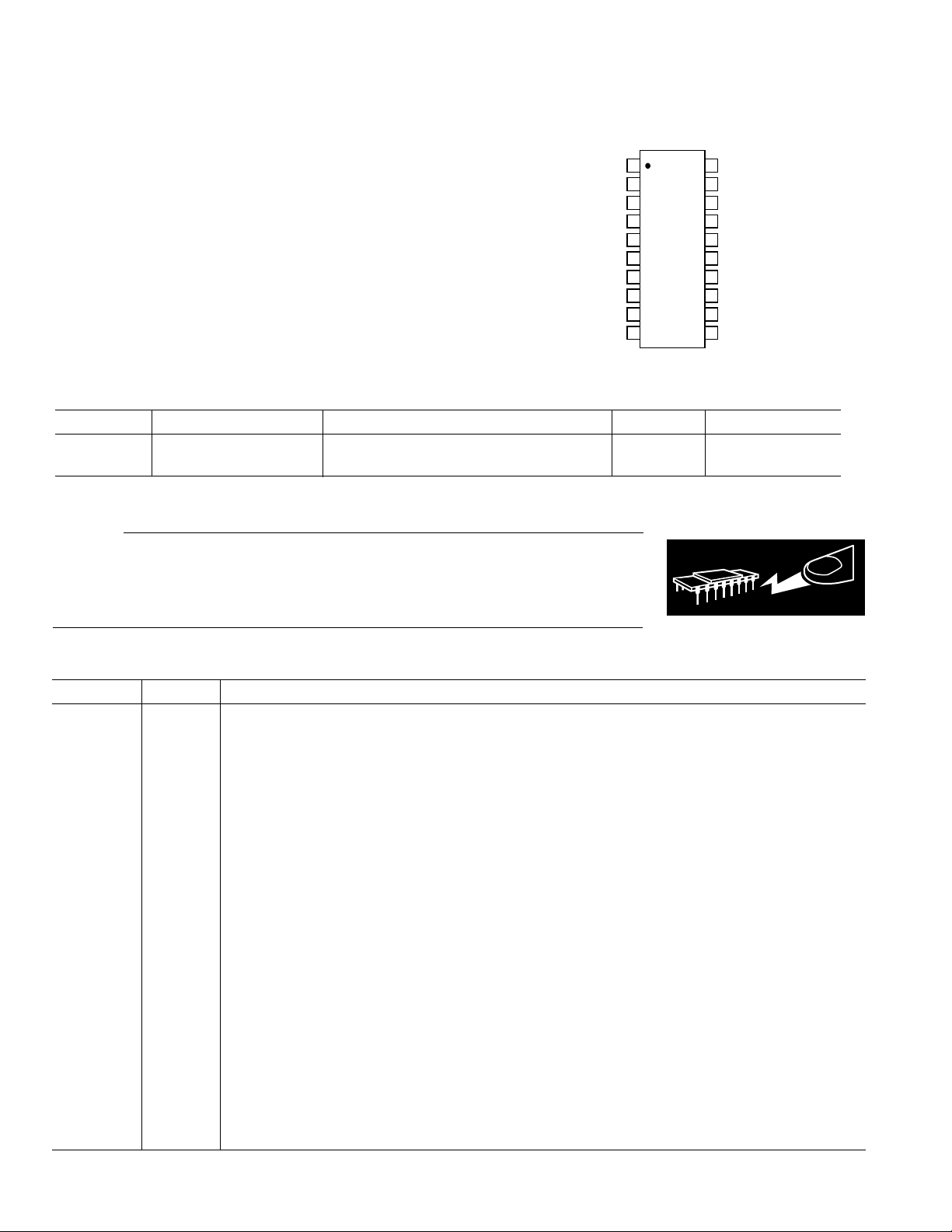
TOP VIEW
(Not to Scale)
20
19
18
17
16
15
14
13
12
11
1
2
3
4
5
6
7
8
9
10
AD8320
VOUT
VCC
VCC
CLK
DATEN
GND
VCC
PD
VOCM
GND
GND
VIN
VREF
VCC
BYP
GND
GND
SDATA
VCC
GND
ABSOLUTE MAXIMUM RATINGS*
Supply Voltage +V
S
PIN CONFIGURATION
Pins 7, 8, 9, 17, 20 . . . . . . . . . . . . . . . . . . . –0.8 V to +13 V
Input Voltages
Pins 19 . . . . . . . . . . . . . . . . . . . . . . . . . . . . . . . . . . . . . ±3 V
Pins 1, 2, 3, 6 . . . . . . . . . . . . . . . . . . . . . . . . –0.8 V to +5 V
Internal Power Dissipation
Small Outline (RP) . . . . . . . . . . . . . . . . . . . . . . . . . . 1.3 W
Operating Temperature Range . . . . . . . . . . . –40°C to +85°C
Storage Temperature Range . . . . . . . . . . . . –65°C to +150°C
Lead Temperature, Soldering 60 seconds . . . . . . . . . . +300°C
*Stresses above those listed under Absolute Maximum Ratings may cause perma-
nent damage to the device. This is a stress rating only; functional operation of the
device at these or any other conditions above those indicated in the operational
section of this specification is not implied. Exposure to absolute maximum rating
conditions for extended periods may affect device reliability.
ORDERING GUIDE
Model Temperature Range Package Description u
JA
Package Option
AD8320ARP –40°C to +85°C 20-Lead Thermally Enhanced Power SOIC* 53°C/W RP-20
AD8320-EB Evaluation Board
*Shipped in tubes (38 pieces/tube) and dry packed per J-STD-020.
CAUTION
ESD (electrostatic discharge) sensitive device. Electrostatic charges as high as 4000 V readily
accumulate on the human body and test equipment and can discharge without detection.
WARNING!
Although the AD8320 features proprietary ESD protection circuitry, permanent damage may
occur on devices subjected to high energy electrostatic discharges. Therefore, proper ESD
precautions are recommended to avoid performance degradation or loss of functionality.
ESD SENSITIVE DEVICE
PIN FUNCTION DESCRIPTIONS
Pin Function Description
1 SDATA Serial Data Input. This digital input allows for an 8-bit serial (gain) word to be loaded into the internal
register with the MSB (most significant bit) first.
2 CLK Clock Input. The clock port controls the serial attenuator data transfer rate to the 8-bit master-slave
register. A Logic 0 to 1 transition latches the data bit and a 1 to 0 transfers the data bit to the slave.
This requires the input serial data word to be valid at or before this clock transition.
3 DATEN Data Enable Low Input. This port controls the 8-bit parallel data latch and shift register. A Logic 0 to 1
transition transfers the latched data to the attenuator core (updates the gain) and simultaneously inhibits serial data transfer into the register. A 1 to 0 transition inhibits the data latch (holds the previous
gain state) and simultaneously enables the register for serial data load.
4, 11, 12,
13, 15, 16 GND Common External Ground Reference.
5 VOCM VCC/2 Reference Pin. A dc output reference level that is equal to 1/2 of the supply voltage (VCC).
This port should be externally ac decoupled (0.1µF cap).
6 PD Power-Down Low Logic Input. A Logic 0 powers down (shuts off) the power amplifier disabling the
output signal and enabling the reverse amplifier. A Logic 1 enables the output power amplifier and
disables the reverse amplifier.
7, 8, 9, 17, 20 VCC Common Positive External Supply Voltage.
10 VOUT Output Signal Port. DC biased to approximately VCC/2.
14 BYP Internal Bypass. This pin must be externally ac decoupled (0.1 µF cap).
18 VREF Input Reference Voltage (typically 1.9 V at 27°C). This port should be externally ac decoupled
19 VIN Analog Voltage Input Signal Port. DC biased to VREF voltage.
(0.1 µF cap).
–4–
REV. 0
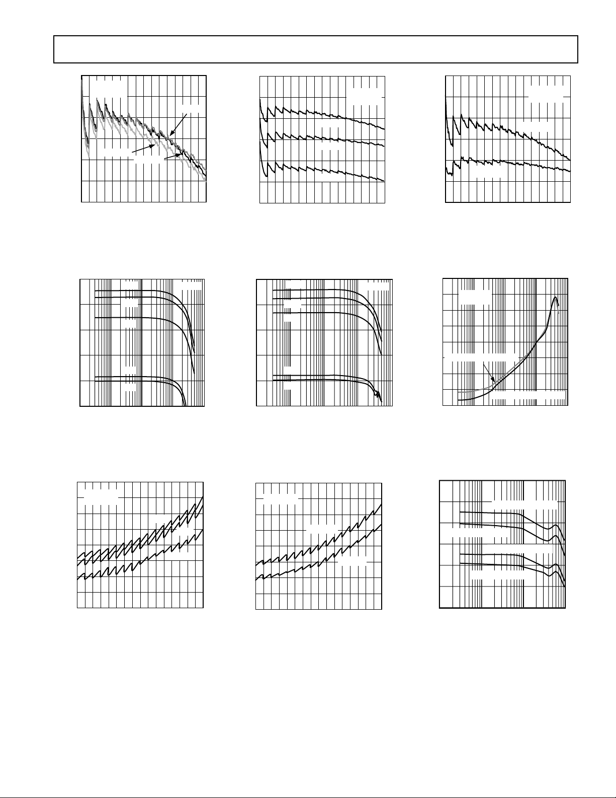
T ypical Performance Characteristics–AD8320
GAIN CONTROL – Decimal
GAIN ERROR – dB
0.45
0
0
20.30
20.15
20.45
64 128 192 256
0.15
F = 10MHz
T = +258C
VCC = 5V
VCC = 12V
0.30
FREQUENCY – Hz
220
100k 1G1M 10M 100M
290
VCC = 12V, PIN = 28dBm
FEEDTHROUGH – dB
VCC = 5V, PIN = 214dBm
MAX GAIN
PD = 0V
230
240
250
260
270
280
2100
0.3
VCC = 12V
F = 10MHz
0.2
0.1
0
20.1
GAIN ERROR – dB
20.2
20.3
T = 2408C
0
GAIN CONTROL – Decimal
T = +858C
64 128 192
T = +258C
256
Figure 4. Gain Error vs. Gain Control
at Various Temperatures
30
20
10
0
GAIN – dB
210
255D
170D
85D
01D
00D
VCC = 5V
0.6
0.3
0
20.3
GAIN ERROR – dB
20.6
20.9
21.2
0
GAIN CONTROL – Decimal
64 128 192 256
VCC = 12V
T = +258C
10MHz
42MHz
65MHz
Figure 5. Gain Error vs. Gain Control
at Various Frequencies
30
20
10
GAIN – dB
0
210
255D
170D
85D
01D
00D
VCC = 12V
Figure 6. Gain Error vs. Gain Control
at Different Supply Voltages
220
100k 1G1M 10M 100M
Figure 7. AC Response
80
F = 10MHz
75
V
CC
70
65
60
55
50
OUTPUT NOISE – nV/!Hz
45
40
064
Figure 10. Output Referred Noise vs.
Gain Control at Various Temperatures
REV. 0
FREQUENCY – Hz
= 12V
+858C
128 192
GAIN CONTROL – Decimal
+258C
2408C
256
220
100k 1G1M 10M 100M
FREQUENCY – Hz
Figure 8. AC Response
80
F = 10MHz
75
70
65
60
55
50
OUTPUT NOISE – nV/!Hz
45
40
064
VCC = 12V
VCC = 5V
GAIN CONTROL – Decimal
128 192
256
Figure 11. Output Referred Noise vs.
Gain Control at Different Supply
Voltages
–5–
Figure 9. Input Signal Feedthrough
vs. Frequency
90
80
70
MAX GAIN, VCC = 5V
60
50
OUTPUT NOISE – nV/!Hz
40
30
100k
MAX GAIN, VCC = 12V
MIN GAIN, VCC = 12V
MIN GAIN, VCC = 5V
1M
FREQUENCY – Hz
10M 100M
Figure 12. Output Referred Noise vs.
Frequency
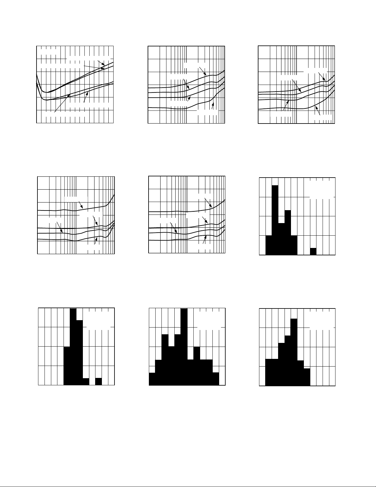
AD8320
230
VCC = 12V
240
F = 42MHz, PO = 18dBm
250
260
270
DISTORTION – dBc
280
F = 65MHz, PO = 12dBm
290
0 64 128 192 256
F = 65MHz, PO = 18dBm
F = 42MHz, PO = 12dBm
GAIN CONTROL – Decimal
Figure 13. Worst Harmonic Distortion vs. Gain Control
220
230
240
250
PO = 8dBm
260
DISTORTION – dBc
270
280
1 10 100
PO = 18dBm
PO = 12dBm
PO = 4dBm
FREQUENCY – MHz
Figure 16. Worst Harmonic Distortion vs. Frequency for Various Output
Levels at VCC = 10 V
220
230
240
250
260
DISTORTION – dBc
270
280
1 10 100
PO = 12dBm
PO = 10dBm
PO = 8dBm
PO = 4dBm
FREQUENCY – MHz
Figure 14. Worst Harmonic Distortion vs. Frequency for Various Output
Levels at VCC = 5 V
220
230
240
250
PO = 8dBm
260
DISTORTION – dBc
270
280
1
FREQUENCY – MHz
PO = 18dBm
PO = 12dBm
PO = 4dBm
10 100
Figure 17. Worst Harmonic Distortion vs. Frequency for Various Output
Levels at VCC = 12 V
220
230
240
250
260
DISTORTION – dBc
270
280
1 10 100
PO = 10dBm
PO = 8dBm
FREQUENCY – MHz
PO = 12dBm
PO = 4dBm
Figure 15. Worst Harmonic Distortion vs. Frequency for Various Output
Levels at VCC = 6 V
40
30
20
PERCENTAGE
10
0
247
HARMONIC DISTORTION – dBc
246 245 244 243
VCC = 12V
= 18dBm
P
O
F = 42MHz
N = 30
Figure 18. Distribution of Worst Harmonic Distortion
40
30
20
PERCENTAGE
10
0
245
HARMONIC DISTORTION 2 dBc
244 243 242 241
VCC = 12V
P
= 18dBm
O
F = 65MHz
N = 30
Figure 19. Distribution of Worst Harmonic Distortion
20
VCC = 12V
P
= 12dBm
O
15
10
PERCENTAGE
5
0
259
HARMONIC DISTORTION 2 dBc
258 257 256 255
F = 42MHz
N = 30
Figure 20. Distribution of Worst Harmonic Distortion
–6–
30.0
22.5
15.0
PERCENTAGE
7.5
0
244
HARMONIC DISTORTION 2 dBc
243 242 241 240
VCC = 5V
P
= 12dBm
O
F = 65MHz
N = 30
Figure 21. Distribution of Worst Harmonic Distortion
REV. 0
 Loading...