

High Speed, Low Power
a
FEATURES
High Speed
50 MHz Unity Gain Stable Operation
300 V/ms Slew Rate
120 ns Settling Time
Drives Unlimited Capacitive Loads
Excellent Video Performance
0.04% Differential Gain @ 4.4 MHz
0.198 Differential Phase @ 4.4 MHz
Good DC Performance
2 mV max Input Offset Voltage
15 mV/8C Input Offset Voltage Drift
Available in Tape and Reel in Accordance with
EIA-481A Standard
Low Power
Only 10 mA Total Supply Current for Both Amplifiers
ⴞ5 V to ⴞ15 V Supplies
PRODUCT DESCRIPTION
The AD827 is a dual version of Analog Devices’ industrystandard AD847 op amp. Like the AD847, it provides high
speed, low power performance at low cost. The AD827 achieves
a 300 V/µs slew rate and 50 MHz unity-gain bandwidth while
consuming only 100 mW when operating from ±5 volt power
supplies. Performance is specified for operation using ±5 V to
±15 V power supplies.
The AD827 offers an open-loop gain of 3,500 V/V into 500 Ω
loads. It also features a low input voltage noise of 15 nV/√Hz,
and a low input offset voltage of 2 mV maximum. Commonmode rejection ratio is a minimum of 80 dB. Power supply
rejection ratio is maintained at better than 20 dB with input
frequencies as high as 1 MHz, thus minimizing noise
feedthrough from switching power supplies.
The AD827 is also ideal for use in demanding video applications, driving coaxial cables with less than 0.04% differential
gain and 0.19° differential phase errors for 643 mV p-p into a
75 Ω reverse terminated cable.
The AD827 is also useful in multichannel, high speed data
conversion systems where its fast (120 ns to 0.1%) settling time
is of importance. In such applications, the AD827 serves as an
input buffer for 8-bit to 10-bit A/D converters and as an output
amplifier for high speed D/A converters.
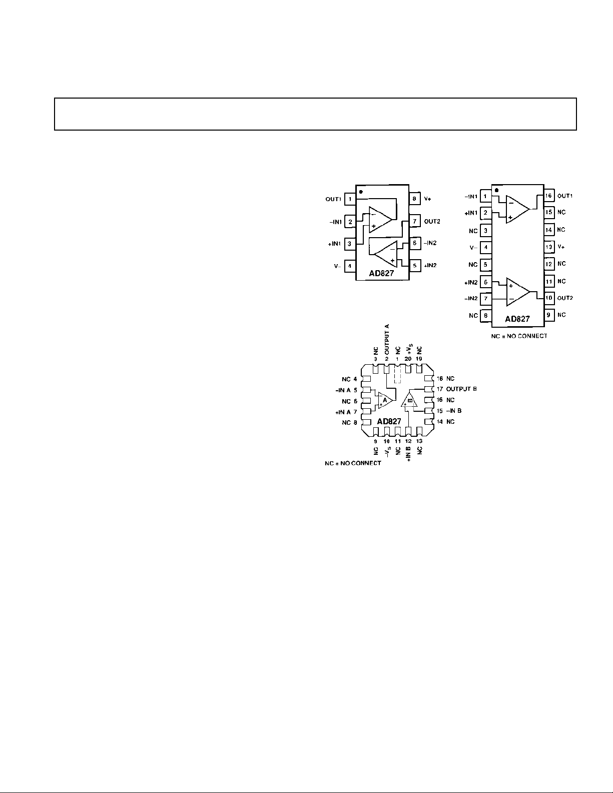
Dual Op Amp
AD827
CONNECTION DIAGRAMS
8-Lead Plastic (N) and Cerdip
(Q) Packages
20-Lead LCC (E) Package
APPLICATION HIGHLIGHTS
1. Performance is fully specified for operation using ±5 V to
±15 V supplies.
2. A 0.04% differential gain and 0.19° differential phase error at
the 4.4 MHz color subcarrier frequency, together with its low
cost, make it ideal for many video applications.
3. The AD827 can drive unlimited capacitive loads, while its
30 mA output current allows 50 Ω and 75 Ω reverse-
terminated loads to be driven.
4. The AD827’s 50 MHz unity-gain bandwidth makes it an
ideal candidate for multistage active filters.
5. The AD827 is available in 8-lead plastic mini-DIP and cerdip,
20-lead LCC, and 16-lead SOIC packages. Chips and
MIL-STD-883B processing are also available.
16-Lead Small Outline
(R) Package
REV. C
Information furnished by Analog Devices is believed to be accurate and
reliable. However, no responsibility is assumed by Analog Devices for its
use, nor for any infringements of patents or other rights of third parties that
may result from its use. No license is granted by implication or otherwise
under any patent or patent rights of Analog Devices.
One Technology Way, P.O. Box 9106, Norwood, MA 02062-9106, U.S.A.
Tel: 781/329-4700 www.analog.com
Fax: 781/326-8703 © Analog Devices, Inc., 2002

AD827–SPECIFICATIONS
(@ TA = +25ⴗC, unless otherwise noted.)
AD827J AD827A/S
Model Conditions V
DC PERFORMANCE
Input Offset Voltage
1
T
to T
MIN
MAX
S
±5 V 0.5 2 0.3 2 mV
Min Typ Max Min Typ Max Unit
3.5 4 mV
±15 V 4 4 mV
to T
T
MIN
MAX
66mV
Offset Voltage Drift ±5 V to ± 15 V 15 15 µV/°C
Input Bias Current ±5 V to ± 15 V 3.3 7 3.3 7 µA
to T
T
MIN
MAX
8.2 9.5 µA
Input Offset Current ±5 V to ± 15 V 50 300 50 300 nA
T
MIN
to T
MAX
400 400 nA
Offset Current Drift ±5 V to ± 15 V 0.5 0.5 nA/°C
Common-Mode Rejection Ratio V
= ±2.5 V ±5 V 78 95 8095 dB
CM
= ±12 V ±15 V 78 95 8095 dB
V
CM
to T
T
MIN
MAX
±5 V to ± 15 V 75 75dB
Power Supply Rejection Ratio ±5 V to ± 15 V 75 86 7586 dB
T
MIN
to T
MAX
72 72 dB
Open-Loop Gain
= ±2.5 V ±5 V
V
O
= 500 Ω 2 3.5 2 3.5 V/mV
R
LOAD
to T
T
R
V
R
T
MIN
LOAD
OUT
LOAD
MIN
MAX
= 150 Ω 1.6 1.6 V/mV
= ±10 V ±15 V
= 1 kΩ 3 5.5 3 5.5 V/mV
to T
MAX
11V/mV
1.5 1.5 V/mV
MATCHING CHARACTERISTICS
Input Offset Voltage ±5 V 0.4 0.2 mV
Crosstalk f = 5 MHz ±5 V 85 85 dB
DYNAMIC PERFORMANCE
Unity-Gain Bandwidth ±5 V 35 35 MHz
Full Power Bandwidth
Slew Rate
3
2
Settling Time to 0.1% A
VO = 5 V p-p,
= 500 Ω±5 V 12.7 12.7 MHz
R
LOAD
= 20 V p-p,
V
O
R
= 1 kΩ±15 V 4.7 4.7 MHz
LOAD
R
= 500 Ω±5 V 200 200 V/µs
LOAD
= 1 kΩ±15 V 300 300 V/µs
R
LOAD
= –1
V
±15 V 50 50 MHz
–2.5 V to +2.5 V ±5 V 65 65 ns
–5 V to +5 V ±15 V 120 120 ns
Phase Margin C
= 10 pF ± 15 V
LOAD
= 1 kΩ 50 50 Degrees
R
LOAD
Differential Gain Error f = 4.4 MHz ± 15 V 0.04 0.04 %
Differential Phase Error f = 4.4 MHz ± 15 V 0.19 0.19 Degrees
Input Voltage Noise f = 10 kHz ±15 V 15 15 nV/√Hz
Input Current Noise f = 10 kHz ± 15 V 1.5 1.5 pA/√Hz
Input Common-Mode
Voltage Range ±5 V +4.3 +4.3 V
–3.4 –3.4 V
±15 V +14.3 +14.3 V
–13.4 –13.4 V
Output Voltage Swing R
= 500 Ω±5 V 3.0 3.6 3.0 3.6 ±V
LOAD
R
= 150 Ω±5 V 2.5 3.0 2.5 3.0 ±V
LOAD
= 1 kΩ±15 V 12 13.3 12 13.3 ±V
R
LOAD
= 500 Ω±15 V 10 12.2 10 12.2 ± V
R
LOAD
Short-Circuit Current Limit ±5 V to ± 15 V 32 32 mA
INPUT CHARACTERISTICS
Input Resistance 300 300 kΩ
Input Capacitance 1.5 1.5 pF
–2–
REV. C
AD827
AD827J AD827A/S
Model Conditions V
S
OUTPUT RESISTANCE Open Loop 15 15 Ω
POWER SUPPLY
Operating Range ±4.5 ± 18 ±4.5 ±18 V
Quiescent Current ±5 V 10 13 1013 mA
to T
T
MIN
MAX
±15 V 10.5 13.5 10.5 13.5 mA
T
to T
MIN
MAX
TRANSISTOR COUNT 92 92
NOTES
1
Offset voltage for the AD827 is guaranteed after power is applied and the device is fully warmed up. All other specifications are measured using high speed test equipment,
approximately 1 second after power is applied.
2
Full Power Bandwidth = Slew Rate/2 π V
3
Gain = +1, rising edge.
All min and max specifications are guaranteed.
Specifications subject to change without notice.
PEAK
.
Min Typ Max Min Typ Max Unit
16 16.5/17.5 mA
16.5 17/18 mA
ABSOLUTE MAXIMUM RATINGS
Supply Voltage . . . . . . . . . . . . . . . . . . . . . . . . . . . . . . . . ±18 V
Internal Power Dissipation
2
1
Plastic (N) Package (Derate at 10 mW/°C) . . . . . . . . 1.5 W
Cerdip (Q) Package (Derate at 8.7 mW/°C) . . . . . . . 1.3 W
Small Outline (R) Package (Derate at 10 mW/°C) . . . 1.5 W
LCC (E) Package (Derate at 6.7 mW/°C) . . . . . . . . . 1.0 W
Input Common-Mode Voltage . . . . . . . . . . . . . . . . . . . . .±V
Differential Input Voltage . . . . . . . . . . . . . . . . . . . . . . . . . 6 V
Output Short Circuit Duration
3
. . . . . . . . . . . . . . . . Indefinite
S
Storage Temperature Range (N, R) . . . . . . . –65°C to +125°C
Storage Temperature Range (Q) . . . . . . . . . –65°C to +150°C
Operating Temperature Range
AD827J . . . . . . . . . . . . . . . . . . . . . . . . . . . . . . 0°C to 70°C
AD827A . . . . . . . . . . . . . . . . . . . . . . . . . . . –40°C to +85°C
AD827S . . . . . . . . . . . . . . . . . . . . . . . . . . –55°C to +125°C
Lead Temperature Range
(Soldering to 60 sec) . . . . . . . . . . . . . . . . . . . . . . . . . 300°C
NOTES
1
Stresses above those listed under Absolute Maximum Ratings may cause permanent damage to the device. This is a stress rating only, and functional operation of
the device at these or any other conditions above those indicated in the operational
section of this specification is not implied. Exposure to absolute maximum ratings
for extended periods may affect device reliability.
2
Maximum internal power dissipation is specified so that TJ does not exceed 175°C
at an ambient temperature of 25°C.
Thermal Characteristics:
MiniDIP: θJA = 100°C/W; θ
Cerdip: θJA = 110°C/W; θ
16-Lead Small Outline Package: θJA = 100°C/W
20-Lead LCC: θJA = 150°C/W; θJC = 35°C/W
3
Indefinite short circuit duration is only permissible as long as the absolute
maximum power rating is not exceeded.
= 33°C/ W
JC
= 30°C/W
JC
ORDERING GUIDE
Temperature Package Package
Model Range Description Option
AD827JN 0°C to +70°C8-Lead Plastic DIP N-8
AD827JR 0°C to +70°C 16-Lead Plastic SO R-16
AD827AQ –40°C to +85°C8-Lead Cerdip Q-8
AD827SQ –55°C to +125°C8-Lead Cerdip Q-8
AD827SQ/883B –55°C to +125°C8-Lead Cerdip Q-8
5962-9211701MPA –55°C to +125°C8-Lead Cerdip Q-8
AD827SE/883B –55°C to +125°C 20-Lead LCC E-20A
5962-9211701M2A –55°C to +125°C 20-Lead LCC E-20A
AD827JR-REEL 0°C to +70°CTape & Reel
AD827JChips 0°C to +70°CDie
AD827SChips –55°C to +125°CDie
METALLIZATION PHOTOGRAPH
Contact factory for latest dimensions.
Dimensions shown in inches and (mm).
Substrate is connected to V+.
REV. C
–3–
AD827
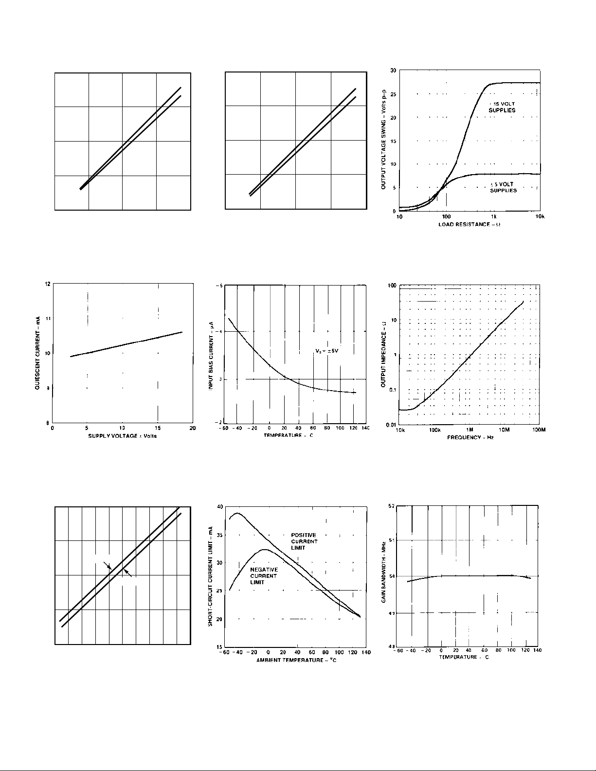
–Typical Performance Characteristics
(@ +25ⴗC & ⴞ15 V, unless otherwise noted)
20
15
+V
IN
10
5
INPUT COMMON-MODE RANGE – Volts
0
051015 20
SUPPLY VOLTAGE ± Volts
–V
IN
Figure1. InputCommon-Mode
Range vs. Supply Voltage
20
15
+V
OUT
10
–V
OUT
R
= 1kΩ
5
OUTPUT VOLTAGE SWING – Volts
0
051015 20
SUPPLY VOLTAGE ± Volts
LOAD
Figure 2. Output Voltage
Swing vs. Supply Voltage
Figure 3. Output Voltage
Swing vs. Load Resistance
Figure 4. Quiescent Current
vs. Supply Voltage
14
12
VS = ±15V
10
QUIESCENT CURRENT – mA
8
0
–60 0 40 100 140
–40 –20 20 60 80 120
VS = ±5V
TEMPERATURE – °C
Figure 7. Quiescent Current
vs. Temperature
Figure 5. Input Bias Current
vs. Temperature
Figure 8. Short-Circuit
Current Limit vs. Temperature
Figure 6. Closed-Loop Output
Impedance vs. Frequency,
Gain = +1
Figure 9. Gain Bandwidth vs.
Temperature
–4–
REV. C

AD827
Figure 10. Open-Loop Gain and
Phase Margin vs. Frequency
Figure 13. Common-Mode
Rejection Ratio vs. Frequency
Figure 11. Open-Loop Gain
vs. Load Resistance
Figure 14. Large Signal
Frequency Response
Figure 12. Power Supply Rejection
Ratio vs. Frequency
Figure 15. Output Swing and
Error vs. Settling Time
400
350
AV = +1
SLEW RATE 10 – 90%
300
250
VS = ±15V
RISE
FALL
RISE
Figure 16. Harmonic Distortion
vs. Frequency
REV. C
Figure 17. Input Voltage
Noise Spectral Density
–5–
200
SLEW RATE – Volts/µs
150
100
–60 –40 –20
Figure 18. Slew Rate vs.
Temperature
VS = ±5V
20 40
0
TEMPERATURE – °C
80 100 120 140
60
FALL

AD827
Figure 19. Crosstalk vs. Frequency
INPUT PROTECTION PRECAUTIONS
An input resistor (resistor RIN of Figure 21a) is recommended in
circuits where the input common-mode voltage to the AD827
may exceed (on a transient basis) the positive supply voltage.
This resistor provides protection for the input transistors by
limiting the maximum current that can be forced into their bases.
Figure 21a. Follower Connection
Figure 21b. Follower Large
Signal Pulse Response
Figure 20. Crosstalk Test Circuit
For high performance circuits, it is recommended that a second
resistor (R
current errors by matching the impedance at each input. This
resistor reduces the error caused by offset voltages by more than
an order of magnitude.
in Figures 21a and 22a) be used to reduce bias-
B
Figure 21c. Follower Small
Signal Pulse Response
Figure 22a. Inverter Connection
Figure 22b. Inverter Large
Signal Pulse Response
–6–
Figure 22c. Inverter Small
Signal Pulse Response
REV. C

AD827
T
VIDEO LINE DRIVER
The AD827 functions very well as a low cost, high speed line
driver for either terminated or unterminated cables. Figure 23
shows the AD827 driving a doubly terminated cable in a
follower configuration.
+V
S
V
IN
50Ω
AD827
0.1 µF
R
500Ω
500Ω
50Ω
BT
R
50Ω
V
OU
T
1/2
0.1 µF
–V
S
C
C
Figure 23. A Video Line Driver
The termination resistor, RT, (when equal to the cable’s
characteristic impedance) minimizes reflections from the far end
of the cable. While operating from ±5 V supplies, the AD827
maintains a typical slew rate of 200 V/µs, which means it can
drive a ±1 V, 30 MHz signal into a terminated cable.
Table I. Video Line Driver Performance Summary
Over-
VIN* V
SUPPLYCC
–3 dB BWshoot
0 dB or ±500 mV Step ± 15 20 pF 23 MHz 4%
0 dB or ±500 mV Step ± 15 15 pF 21 MHz 0%
0 dB or ±500 mV Step ± 15 0 pF 13 MHz 0%
0 dB or ±500 mV Step ± 5 20 pF 18 MHz 2%
0 dB or ±500 mV Step ± 5 15 pF 16 MHz 0%
0 dB or ±500 mV Step ± 50 pF11 MHz 0%
*–3 dB bandwidth numbers are for the 0 dBm signal input. Overshoot numbers
are the percent overshoot of the 1 V step input.
A back-termination resistor (RBT, also equal to the characteristic
impedance of the cable) may be placed between the AD827
output and the cable input, in order to damp any reflected
signals caused by a mismatch between R
and the cable’s
T
characteristic impedance. This will result in a flatter frequency
response, although this requires that the op amp supply ±2 V to
the output in order to achieve a ±1 V swing at resistor R
.
T
A HIGH SPEED THREE OP AMP INSTRUMENTATION AMPLIFIER CIRCUIT
The instrumentation amplifier circuit shown in Figure 24 can
provide a range of gains. Table II details performance.
+V
S
0.1µF
–V
IN
3
8
+
1
1/2
AD827
2
–
1kΩ
TRIM FOR
R
OPTIMUM
G
BANDWIDTH
7 – 15 pF
1kΩ
6
–
1/2
AD827
+V
IN
5
+
4
0.1µF
–V
S
2kΩ
2kΩ
3pF
7
NOTE: PINOUT SHOWN IS FOR MINIDIP PACKAGE
TRIM FOR BEST
SETTLING TIME
2 – 8pF
2kΩ
+V
S
0.1µF
7
2
–
AD847
3
+
4
0.1µF
2kΩ
–V
S
CIRCUIT GAIN =
6
2000
R
V
OUT
2kΩ
R
L
+ 1
G
Figure 24. A High Bandwidth Three Op Amp
Instrumentation Amplifier
Table II. Performance Specifications for the
Three Op Amp Instrumentation Amplifier
Small Signal
Bandwidth
Gain R
G
@ 1 V p-p Output
1 Open 16.1 MHz
22 k 14.7 MHz
10 226 Ω 4.9 MHz
100 20 Ω 660 kHz
REV. C
–7–
AD827
A TWO-CHIP VOLTAGE-CONTROLLED AMPLIFIER (VCA) WITH EXPONENTIAL RESPONSE
Voltage-controlled amplifiers are often used as building blocks
in automatic gain control systems. Figure 25 shows a two-chip
VCA built using the AD827 and the AD539, a dual, currentoutput multiplier. As configured, the circuit has its two
Figure 25. A Wide Range Voltage-Controlled
Amplifier Circuit
multipliers connected in series. They could also be placed in
parallel with an increase in bandwidth and a reduction in gain.
The gain of the circuit is controlled by V
from 0 to 3 V dc. Measurements show that this circuit easily
supplies 2 V p-p into a 100 Ω load while operating from ±5 V
supplies. The overall bandwidth of the circuit is approximately
7 MHz with 0.5 dB of peaking.
Each half of the AD827 serves as an I/V converter and converts
the output current of one of the two multipliers in the AD539
into an output voltage. Each of the AD539’s two multipliers
contains two internal 6 kΩ feedback resistors; one is connected
, which can range
X
between the CH1 output and Z1, the other between the CH1
output and W1. Likewise, in the CH2 multiplier, one of the
feedback resistors is connected between CH2 and Z2 and the
other is connected between CH2 and Z2. In Figure 25, Z1 and
W1 are tied together, as are Z2 and W2, providing a 3 kΩ
feedback resistor for the op amp. The 2 pF capacitors connected
between the AD539’s W1 and CH1 and W2 and CH2 pins are
in parallel with the feedback resistors and thus reduce peaking
in the VCA’s frequency response. Increasing the values of C3
and C4 can further reduce the peaking at the expense of
reduced bandwidth. The 1.25 mA full-scale output current of
the AD539 and the 3 kΩ feedback resistor set the full-scale
output voltage of each multiplier at 3.25 V p-p.
Current limiting in the AD827 (typically 30 mA) limits the output voltage in this application to about 3 V p-p across a 100 Ω
load. Driving a 50 Ω reverse-terminated load divides this value
by two, limiting the maximum signal delivered to a 50 Ω load to
about 1.5 V p-p, which suffices for video signal levels. The
dynamic range of this circuit is approximately 55 dB and is
primarily limited by feedthrough at low input levels and by the
maximum output voltage at high levels.
Guidelines for Grounding and Bypassing
When designing practical high frequency circuits using the AD827,
some special precautions are in order. Both short interconnection
leads and a large ground plane are needed whenever possible to
provide low resistance, low inductance circuit paths. One should
remember to minimize the effects of capacitive coupling
between circuits. Furthermore, IC sockets should be avoided.
Feedback resistors should be of a low enough value that the
time constant formed with stray circuit capacitances at the
amplifier summing junction will not limit circuit performance.
As a rule of thumb, use feedback resistor values that are less
than 5 kΩ. If a larger resistor value is necessary, a small (<10 pF)
feedback capacitor in parallel with the feedback resistor may be
used. The use of 0.1 µF ceramic disc capacitors is recommended
for bypassing the op amp’s power supply leads.
–8–
REV. C

OUTLINE DIMENSIONS
1
4
85
7.87 (0.3089)
5.59 (0.2201)
PIN 1
0.13 (0.0051)
MIN
1.40 (0.0551)
MAX
2.54 (0.1000) BSC
15
0
8.13 (0.3201)
7.37 (0.2902)
0.38 (0.0150)
0.20 (0.0079)
SEATING
PLANE
5.08 (0.2000)
MAX
10.29 (0.4051) MAX
3.81 (0.1500)
MIN
5.08 (0.2000)
3.18 (0.1252)
0.58 (0.0228)
0.36 (0.0142)
1.78 (0.0701)
0.76 (0.0299)
1.52 (0.0600)
0.38 (0.0150)
CONTROLLING DIMENSIONS ARE IN MILLIMETERS; INCH DIMENSIONS
(IN PARENTHESES) ARE ROUNDED-OFF MILLIMETER EQUIVALENTS FOR
REFERENCE ONLY AND ARE NOT APPROPRIATE FOR USE IN DESIGN
1
20
4
9
8
13
19
14
3
18
BOTTOM
VIEW
0.71 (0.0278)
0.56 (0.0220)
45 TYP
0.38 (0.0150)
MIN
1.40 (0.0551)
1.14 (0.0449)
1.27 (0.0500)
BSC
1.91 (0.0752)
REF
0.28 (0.0110)
0.18 (0.0071)
R TYP
2.41 (0.0949)
1.90 (0.0748)
2.54 (0.1000) BSC
5.08 (0.2000)
BSC
3.81 (0.1500)
BSC
1.91
(0.0752)
REF
9.09 (0.3579)
8.69 (0.3421)
SQ
9.09
(0.3579)
MAX
SQ
2.54 (0.1000)
1.63 (0.0642)
2.24 (0.0882)
1.37 (0.0539)
CONTROLLING DIMENSIONS ARE IN MILLIMETERS; INCH DIMENSIONS
(IN PARENTHESES) ARE ROUNDED-OFF MILLIMETER EQUIVALENTS FOR
REFERENCE ONLY AND ARE NOT APPROPRIATE FOR USE IN DESIGN
AD827
8-Lead Plastic Dual-in-Line Package [PDIP]
(N-8)
Dimensions shown in millimeters and (inches)
10.92 (0.4299)
8.84 (0.3480)
8
PIN 1
2.54 (0.1000)
5.33
(0.2098)
MAX
4.06 (0.1598)
2.93 (0.1154)
0.56 (0.0220)
0.36 (0.0142)
CONTROLLING DIMENSIONS ARE IN MILLIMETERS; INCH DIMENSIONS
(IN PARENTHESES) ARE ROUNDED-OFF MILLIMETER EQUIVALENTS FOR
REFERENCE ONLY AND ARE NOT APPROPRIATE FOR USE IN DESIGN
1
BSC
1.77 (0.0697)
1.15 (0.0453)
5
7.11 (0.2799)
6.10 (0.2402)
4
1.52 (0.0598)
0.38 (0.0150)
(
3.30
(0.1299)
MIN
SEATING
PLANE
8.25 (0.3248)
7.62 (0.3000)
4.95 (0.1949)
2.93 (0.1154)
0.38 (0.0150)
0.20 (0.0079)
16-Lead Standard Small Outline Package [SOIC]
Wide Body
(R-16)
Dimensions shown in millimeters and (inches)
10.50 (0.4134)
10.10 (0.3976)
8-Lead Ceramic DIP-Glass Hermetic Seal Package [CERDIP]
(Q-8)
Dimensions shown in millimeters and (inches)
20-Terminal Ceramic Leadless Chip Carrier [LCC]
(E-20A)
Dimensions shown in millimeters and (inches)
9
8
2.65 (0.1043)
2.35 (0.0925)
SEATING
PLANE
7.60 (0.2992)
7.40 (0.2913)
10.65 (0.4193)
10.00 (0.3937)
0.32 (0.0126)
0.23 (0.0091)
16
1
PIN 1
1.27 (0.0500)
BSC
0.51 (0.0201)
0.33 (0.0130)
0.30 (0.0118)
0.10 (0.0039)
COPLANARITY
0.10
CONTROLLING DIMENSIONS ARE IN MILLIMETERS; INCH DIMENSIONS
(IN PARENTHESES) ARE ROUNDED-OFF MILLIMETER EQUIVALENTS FOR
REFERENCE ONLY AND ARE NOT APPROPRIATE FOR USE IN DESIGN
COMPLIANT TO JEDEC STANDARDS MS-013AA
REV. C
0.75 (0.0295)
0.25 (0.0098)
8ⴗ
0ⴗ
ⴛ 45ⴗ
1.27 (0.0500)
0.40 (0.0157)
–9–

AD827
Revision History
Location Page
8/02—Data Sheet changed from REV. B to REV. C.
Updated Outline Dimensions . . . . . . . . . . . . . . . . . . . . . . . . . . . . . . . . . . . . . . . . . . . . . . . . . . . . . . . . . . . . . . . . . . . . . . . . . . . . . .9
–10–
REV. C

–11–

C00878–0–8/02(C)
–12–
PRINTED IN U.S.A.
 Loading...