

Page 1
Instrumentation Amplifier
AD8237
Rev. 0
on furnished by Analog Devices is believed to be accurate and reliable. However, no
Trademarks and registered trademarks are the property of their respective owners.
Fax: 781.461.3113 ©2012 Analog Devices, Inc. All rights reserved.
BW
1
+IN
2
–IN
3
–V
S
4
V
OUT
8
FB
7
REF
6
+V
S
5
AD8237
TOP VIEW
(Not to S cale)
+
–
–
+
10289-001
6
5
4
3
2
1
–1
0
0 1 2 3 4 5
INPUT COMMON-MODE VOLTAGE (V)
OUTPUT VOLTAGE (V)
TRADITI ONAL IN-AMP
(RAIL-TO-RAIL OUT)
AD8237
10289-002
G = 100
V
S
= 5V
V
REF
= 2.5V
Data Sheet
FEATURES
Gain set with 2 external resistors
Can achieve low gain drift at all gains
Ideal for battery powered instruments
Supply current: 115 µA
Rail-to-rail input and output
Zero input crossover distortion
Designed for excellent dc performance
Minimum CMRR: 106 dB
Maximum offset voltage drift: 0.3 µV/°C
Maximum gain error: 0.005% (all gains)
Maximum gain drift: 0.5 ppm/°C (all gains)
Input bias current: 1 nA guaranteed to 125°C
Bandwidth mode pin (BW) to adjust compensation
8 kV HBM ESD rating
RFI filter on-chip
Single-supply operation: 1.8 V to 5.5 V
8-lead MSOP package
APPLICATIONS
Bridge amplification
Pressure measurement
Medical instrumentation
Thermocouple interface
Portable systems
Current measurement
GENERAL DESCRIPTION
The AD8237 is a micropower, zero drift, rail-to-rail input and
output instrumentation amplifier. The relative match of two
resistors sets any gain from 1 to 1000. The AD8237 has excellent
gain accuracy performance that can be preserved at any gain
with two ratio-matched resistors.
The AD8237 employs the indirect current feedback architecture to
achieve a true rail-to-rail capability. Unlike conventional in-amps,
the AD8237 can fully amplify signals with common-mode voltage
at or even slightly beyond its supplies. This enables applications
with high common-mode voltages to use smaller supplies and
save power.
The AD8237 is an excellent choice for portable systems. With a
minimum supply voltage of 1.8 V, a 115 µA typical supply current,
and wide input range, the AD8237 makes full use of a limited
power budget, yet offers bandwidth and drift performance suitable
for bench-top systems.
Infor mati
responsibility is assumed by Analog Devices for its use, nor for any infringements of patents or other
rights of third parties that may result from its use. Specifications subject to change without notice. No
license is granted by implication or otherwise under any patent or patent rights of Analog Devices.
Micropower, Zero Drift, True Rail-to-Rail
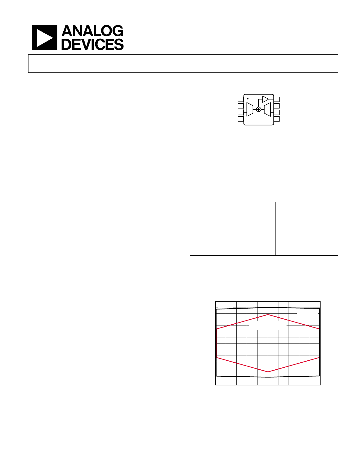
PIN CONFIGURATION
Figure 1.
Table 1. Instrumentation Amplifiers by Category
General
Purpose
AD8421 AD8237 AD620 AD8237 AD8250
AD8221/AD8222 AD8231 AD621 AD8420 AD8251
AD8220/AD8224 AD8293 AD524 AD8235/AD8236 AD8253
AD8228 AD8553 AD526 AD627 AD8231
AD8295 AD8556 AD624
AD8226 AD8557
1
See www.analog.com for the latest instrumentation amplifiers.
Zero
Drift
Military
Grade
Micropower
The AD8237 is available in an 8-lead MSOP package. Performance
is specified over the full temperature range of −40°C to +125°C.
Figure 2. Input Common-Mode Voltage vs. Output Vo ltage, +V
One Technology Way, P.O. Box 9106, Norwood, MA 02062-9106, U.S.A.
Tel: 781.329.4700
1
Digital
Gain
= 5 V, G = 100
S
www.analog.com
Page 2

AD8237 Data Sheet
TABLE OF CONTENTS
Features .............................................................................................. 1
Applications ....................................................................................... 1
Pin Configuration ............................................................................. 1
General Description ......................................................................... 1
Revision History ............................................................................... 2
Specifications ..................................................................................... 3
Absolute Maximum Ratings ............................................................ 7
Thermal Resistance ...................................................................... 7
ESD Caution .................................................................................. 7
Pin Configuration and Function Descriptions ............................. 8
Typical Performance Characteristics ............................................. 9
Theory of Operation ...................................................................... 20
Architecture ................................................................................. 20
Setting the Gain .......................................................................... 20
Gain Accuracy............................................................................. 21
Clock Feedthrough ..................................................................... 21
Input Voltage Range ................................................................... 21
Input Protection ......................................................................... 22
Filtering Radio Frequency Interference .................................. 22
Using the Reference Pin ............................................................ 22
Layout .......................................................................................... 23
Input Bias Current Return Path ............................................... 23
Applications Information .............................................................. 25
Battery Current Monitor ........................................................... 25
Programmable Gain In-Amp.................................................... 25
AD8237 in an Electrocardiogram (ECG) Front End............. 26
Outline Dimensions ....................................................................... 27
Ordering Guide .......................................................................... 27
REVISION HISTORY
8/12—Revision 0: Initial Version
Rev. 0 | Page 2 of 28
Page 3

Data Sheet AD8237
COMMON-MODE REJECTION RATIO (CMRR)
VCM = 0.1 V to 4.9 V
CMRR at 1 kHz
80 dB
Input Bias Current
TA = +25°C
250
650
pA
Low Bandwidth Mode
Pin 1 connected to −VS
SPECIFICATIONS
+VS = +5 V, − VS = 0 V, V
otherwise noted.
Table 2.
Parameter Test Conditions/Comments Min Typ Max Unit
CMRR at DC
G = 1, G = 10 106 120 dB
G = 100, G = 1000 114 140 dB
Over Temperature (G = 1) TA = −40°C to +125°C 104 dB
NOISE
Voltage Noise
Spectral Density f = 1 kHz 68 nV/√Hz
Peak to Peak f = 0.1 Hz to 10 Hz 1.5 µV p-p
Current Noise
Spectral Density f = 1 kHz 70 fA/√Hz
Peak to Peak f = 0.1 Hz to 10 Hz 3 pA p-p
VOLTAGE OFFSET
Offset 30 75 µV
Average Temperature Coefficient TA = −40°C to +125°C 0.3 µV/°C
Offset RTI vs. Supply (PSR) 100 dB
INPUTS1 Valid for REF and FB pair, as well as +IN and −IN
= 2.5 V, VCM = 2.5 V, TA = 25°C, G = 1 to 1000, RL = 10 kΩ to ground, specifications referred to input, unless
REF
Over Temperature TA = −40°C to +125°C 1 nA
Average Temperature Coefficient 0.5 pA/°C
Input Offset Current TA = +25°C 250 650 pA
Over Temperature TA = −40°C to +125°C 1 nA
Average Temperature Coefficient 0.5 pA/°C
Input Impedance
Differential 100||5 MΩ||pF
Common Mode 800||10 MΩ||pF
Differential Input Operating Voltage TA = −40°C to +125°C ±3.85 V
Input Operating Voltage (+IN, −IN, or REF) TA = +25°C −VS − 0.3 +VS + 0.3 V
TA = −40°C to +125°C −VS − 0.2 +VS + 0.2 V
DYNAMIC RESPONSE
Small Signal Bandwidth −3 dB
G = 1 200 kHz
G = 10 20 kHz
G = 100 2 kHz
G = 1000 0.2 kHz
High Bandwidth Mode Pin 1 connected to +VS
G = 10 100 kHz
G = 100 10 kHz
G = 1000 1 kHz
Rev. 0 | Page 3 of 28
Page 4

AD8237 Data Sheet
G = 100
440 µs
OUT
CM
Gain vs. Temperature
TA = −40°C to +125°C
0.5
ppm/°C
OUT
Parameter Test Conditions/Comments Min Typ Max Unit
Settling Time 0.01% 4 V output step
Low Bandwidth Mode Pin 1 connected to −VS
G = 1 80 µs
G = 10 100 µs
G = 1000 4 ms
High Bandwidth Mode Pin 1 connected to +VS
G = 10 80 µs
G = 100 100 µs
G = 1000 820 µs
Slew Rate
Low Bandwidth Mode 0.05 V/µs
High Bandwidth Mode 0.15 V/µs
EMI Filter Frequency 6 MHz
GAIN2 G = 1 + (R2/R1)
Gain Range3 1 1000 V/V
Gain Error V
Gain Error vs. V
= 0.1 V to 4.9 V, G = 1 to G = 1000 0.005 %
15 ppm/V
Gain Nonlinearity V
= 0.2 V to 4.8 V, RL = 10 kΩ to ground
G = 1, G = 10 3 ppm
G = 100 6 ppm
G = 1000 10 ppm
OUTPUT
Output Swing
RL = 10 kΩ to Midsupply TA = +25°C −VS + 0.05 +VS − 0.05 V
TA = −40°C to 125°C −VS + 0.07 +VS − 0.07 V
RL = 100 kΩ to Midsupply TA = +25°C −VS + 0.02 +VS − 0.02 V
TA = −40°C to 125°C −VS + 0.03 +VS − 0.03 V
Short-Circuit Current 4 mA
POWER SUPPLY
Operating Range 1.8 5.5 V
Quiescent Current TA = +25°C 115 130 µA
TA = −40°C to +125°C 150 µA
TEMPERATURE RANGE
Specified −40 +125 °C
1
Specifications apply to input voltages between 0 V and 5 V. When measuring voltages beyond the supplies, there is additional offset error, bias currents increase, and
input impedance decreases, especially at higher temperatures.
2
For G > 1, errors from the external resistors, R1 and R2, must be added to these specifications, including error from the FB pin bias current.
3
The AD8237 has only been characterized for gains of 1 to 1000; however, higher gains are possible.
Rev. 0 | Page 4 of 28
Page 5

Data Sheet AD8237
G = 1, G = 10
100
120 dB
DIFF
DIFF
VOLTAGE OFFSET
Average Temperature Coefficient
0.5 pA/°C
G = 10
20 kHz
+VS = 1.8 V, −VS = 0 V, V
otherwise noted.
Table 3.
Parameter Test Conditions/Comments Min Typ Max Unit
COMMON-MODE REJECTION RATIO (CMRR) VCM = 0.2 V to 1.6 V
CMRR at DC
G = 100, G = 1000 114 140 dB
Over Temperature (G = 1) TA = −40°C to +125°C 94 dB
CMRR at 1 kHz 80 dB
NOISE
Voltage Noise
Spectral Density f = 1 kHz, V
Peak to Peak f = 0.1 Hz to 10 Hz, V
Current Noise
Spectral Density f = 1 kHz 70 fA/√Hz
Peak to Peak f = 0.1 Hz to 10 Hz 3 pA p-p
Offset 25 75 µV
Average Temperature Coefficient TA = −40°C to +125°C 0.3 µV/°C
Offset RTI vs. Supply (PSR) 100 dB
INPUTS1 Valid for REF and FB pair, as well as +IN and −IN
Input Bias Current TA = +25°C 250 650 pA
Over Temperature TA = −40°C to +125°C 1 nA
= 0.9 V, VCM = 0.9 V, TA = 25°C, G = 1 to 1000, RL = 10 kΩ to ground, specifications referred to input, unless
REF
≤ 100 mV 68 nV/√Hz
≤ 100 mV 1.5 µV p-p
Input Offset Current TA = +25°C 250 650 pA
Over Temperature TA = −40°C to +125°C 1 nA
Average Temperature Coefficient 0.5 pA/°C
Input Impedance
Differential 100||5 MΩ||pF
Common Mode 800||10 MΩ||pF
Differential Input Operating Voltage TA = −40°C to +125°C ± 0.75 V
Input Operating Voltage (+IN, −IN, REF, or FB) TA = +25°C −VS − 0.3 +VS + 0.3 V
TA = −40°C to +125°C −VS − 0.2 +VS + 0.2 V
DYNAMIC RESPONSE
Small Signal Bandwidth −3 dB
Low Bandwidth Mode Pin 1 connected to −VS
G = 1 200 kHz
G = 100 2 kHz
G = 1000 0.2 kHz
High Bandwidth Mode Pin 1 connected to +VS
G = 10 100 kHz
G = 100 10 kHz
G = 1000 1 kHz
Slew Rate
Low Bandwidth Mode 0.05 V/µs
High Bandwidth Mode 0.15 V/µs
EMI Filter Frequency 6 MHz
Rev. 0 | Page 5 of 28
Page 6

AD8237 Data Sheet
OUT
CM
Gain vs. Temperature
TA = −40°C to +125°C
0.5
ppm/°C
OUT
RL = 100 kΩ to Midsupply
TA = +25°C
−VS + 0.02
+VS − 0.02
V
Parameter Test Conditions/Comments Min Typ Max Unit
GAIN2 G = 1 + (R2/R1)
Gain Range3 1 1000 V/V
Gain Error V
Gain Error vs. V
= 0.2 V to 1.6 V, G = 1 to G = 1000 0.005 %
15 ppm/V
Gain Nonlinearity V
= 0.2 V to 1.6 V
G = 1, G = 10 3 ppm
G = 100 6 ppm
G = 1000 10 ppm
OUTPUT
Output Swing
RL = 10 kΩ to Midsupply TA = +25°C −VS + 0.05 +VS − 0.05 V
TA = −40°C to 125°C −VS + 0.07 +VS − 0.07 V
TA = −40°C to 125°C −VS + 0.03 +VS − 0.03 V
Short-Circuit Current 4 mA
POWER SUPPLY
Operating Range 1.8 5.5 V
Quiescent Current TA = +25°C 115 130 µA
TA = −40°C to +125°C 150 µA
TEMPERATURE RANGE
Specified −40 +125 °C
1
Specifications apply to input voltages between 0 V and 1.8 V. When measuring voltages beyond the supplies, there is additional offset error, bias currents increase,
and input impedance decreases, especially at higher temperatures.
2
For G > 1, errors from the external resistors, R1 and R2, must be added to these specifications, including error from the FB pin bias current.
3
The AD8237 has only been characterized for gains of 1 to 1000; however, higher gains are possible.
Rev. 0 | Page 6 of 28
Page 7
Data Sheet AD8237
Human Body Model
8 kV
ABSOLUTE MAXIMUM RATINGS
Table 4.
Parameter Rating
Supply Voltage 6 V
Output Short-Circuit Current Duration Indefinite
Maximum Voltage at −IN, +IN, FB, or REF1 +VS + 0.5 V
Minimum Voltage at −IN, +IN, FB, or REF1 −VS − 0.5 V
Storage Temperature Range −65°C to +150°C
Junction Temperature Range −65°C to +150°C
ESD
Charge Device Model 1.25 kV
Machine Model 0.2 kV
1
If input voltages beyond the specified minimum or maximum voltages are
expected, place resistors in series with the inputs to limit the current to 5 mA.
Stresses above those listed under Absolute Maximum Ratings
may cause permanent damage to the device. This is a stress
rating only; functional operation of the device at these or any
other conditions above those indicated in the operational
section of this specification is not implied. Exposure to absolute
maximum rating conditions for extended periods may affect
device reliability.
THERMAL RESISTANCE
θJA is specified for a device in free air.
Table 5.
Package θJA Unit
8-Lead MSOP, 4-Layer JEDEC Board 145.7 °C/W
ESD CAUTION
Rev. 0 | Page 7 of 28
Page 8

AD8237 Data Sheet
BW
1
+IN
2
–IN
3
–V
S
4
V
OUT
8
FB
7
REF
6
+V
S
5
AD8237
TOP VIEW
(Not to S cale)
+
–
–
+
10289-003
7
FB
Feedback Input.
OUT
PIN CONFIGURATION AND FUNCTION DESCRIPTIONS
Figure 3. Pin Configuration
Table 6. Pin Function Descriptions
Pin No. Mnemonic Description
1 BW For high bandwidth mode, connect this pin to +VS, or for low bandwidth mode, connect this pin to −VS. Do not
leave this pin floating.
2 +IN Positive Input.
3 −IN Negative Input.
4 −VS Negative Supply.
5 +VS Positive Supply.
6 REF Reference Input.
8 V
Output.
Rev. 0 | Page 8 of 28
Page 9
Data Sheet AD8237
16
14
12
8
10
6
4
2
0
–60 –20–40 0 20 40 60
UNITS
OFFSET VOLTAGE (µV)
10289-004
18
21
15
12
9
6
3
0
–0.6 –0.4 –0.2 0 0.2 0.4 0.6
UNITS
POSIT IVE INPUT BIAS CURRENT (n A)
10289-005
35
30
20
25
15
10
5
0
–60 –20–40 0 20 40 60
UNITS
GAIN ERROR ( µ V /V)
10289-006
30
35
40
25
20
15
10
5
0
–6 –4 –2 0 2 4 6
UNITS
CMRR (µV/V)
10289-007
18
15
12
9
6
3
0
–0.6 –0.4 –0.2 0 0.2 0.4 0.6
UNITS
INPUT OFFSET CURRENT (nA)
10289-008
24
18
21
12
15
9
6
3
0
100 110105 115 120 125 130
UNITS
SUPPLY CURRENT (µA)
10289-009
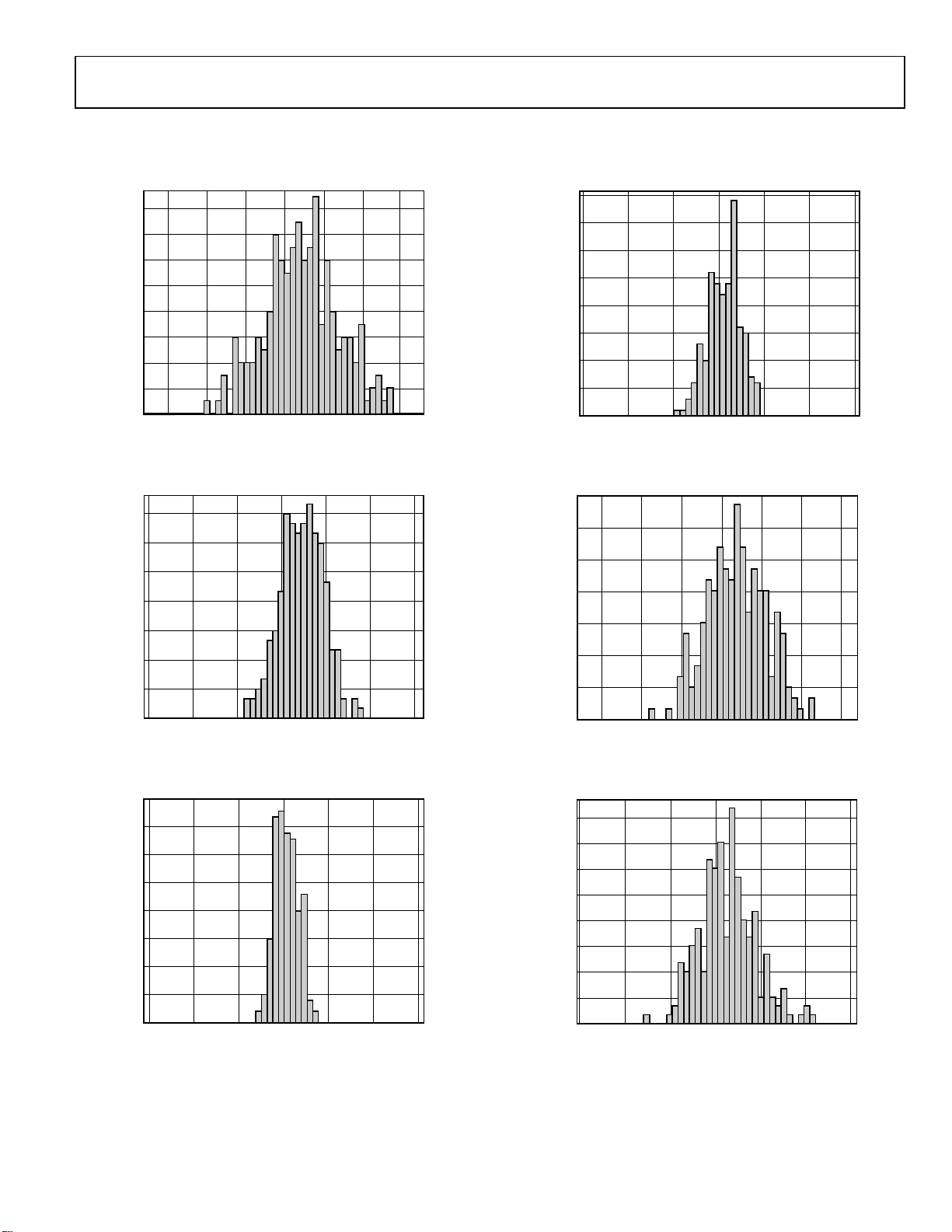
TYPICAL PERFORMANCE CHARACTERISTICS
+VS = +5 V, −VS = 0 V, V
= 2.5 V, TA = 25°C, RL = 10 kΩ to ground, unless otherwise noted.
REF
Figure 4. Typical Distribution of Offset Voltage
Figure 5. Typical Distribution of Input Bias Current
Figure 7. Typical Distribution of CMRR
Figure 8. Typical Distribution of Input Offset Current
Figure 6. Typical Distribution of Gain Error (G = 1)
Rev. 0 | Page 9 of 28
Figure 9. Typical Distribution of Supply Current
Page 10

AD8237 Data Sheet
6
5
–1
0
1
2
3
4
0 0.5 1.0 1.5 2.0 2.5 3.0 3.5 4.0 4.5
COMMON-MODE VOLTAGE (V)
OUTPUT VOLTAGE (V)
VS = 1.8V
V
S
= 5V
G = 1
V
REF
= 0V
R
L
= 10kΩ
10289-010
6
5
–1
0
1
2
3
4
0 1 2 3 4 5 6
COMMON-MODE VOLTAGE (V)
OUTPUT VOLTAGE (V)
V
S
= 1.8V
VS = 5V
G = 100
V
REF
= 0V
R
L
= 10kΩ
10289-011
4
3
2
1
–4
–3
–2
–1
0
–3 3210–1–2
COMMON-MODE VOLTAGE (V)
VOLTAGE OUTPUT (V)
G = 1
V
REF
= 0V
R
L
= 5kΩ
V
S
= ±2.5V
V
S
= ±0.9V
10289-012
4
3
2
1
–4
–3
–2
–1
0
–3 3210–1–2
COMMON-MODE VOLTAGE (V)
OUTPUT VOLTAGE (V)
V
S
= ±2.5V
VS = ±0.9V
G = 100
V
REF
= 0V
R
L
= 5kΩ
10289-013
5.0
4.5
4.0
0.5
1.0
1.5
2.0
2.5
3.0
3.5
0
1.8 2.3 2.8 3.3 3.8 4.3 4.8
V
IN
(V)
SUPPLY VOLTAGE (V)
–40°C
+25°C
+85°C
+105°C
+125°C
10289-014
5
–5
–3.0 3.0
INPUT BIAS CURRE NT (nA)
COMMON-MODE VOLTAGE (V)
–4
–3
–2
–1
0
1
2
3
4
–2.5 –2.0 –1.5 –1.0 –0.5 0 0.5 1.0 1.5 2.0 2.5
+V
S
–V
S
I
B
+
I
B
–
10289-015
REPRESENTATIVE SAMPLE
Figure 10. Input Common-Mode Voltage vs. Output Voltage,
G = 1, V
= 0 V, VS = 5 V and VS = 1.8 V, RL = 10 kΩ to Ground
REF
Figure 11. Input Common-Mode Voltage vs. Output Voltage,
G = 100, V
= 0 V, VS = 5 V and VS = 1.8 V, RL = 10 kΩ to Ground
REF
Figure 13. Input Common-Mode Voltage vs. Output Voltage,
G = 100, V
= 0 V, VS = ±2.5 V and VS = ±0.9 V, RL = 5 kΩ to Ground
REF
Figure 14. Maximum Differential Input vs. Supply Voltage
Figure 12. Input Common-Mode Voltage vs. Output Voltage,
G = 1, V
= 0 V, VS = ±2.5 V and VS = ±0.9 V, RL = 5 kΩ to Ground
REF
Figure 15. Input Bias Current vs. Common-Mode Voltage
Rev. 0 | Page 10 of 28
Page 11

Data Sheet AD8237
15
–15
–2.5 2.5
INPUT BIAS CURRE NT (nA)
DIFFERENTIAL INPUT VOLTAGE (V)
–10
–5
0
5
10
–2.0 –1.5 –1.0 –0.5 0 0.5 1.0 1.5 2.0
I
B
+
I
B
–
V
S
= ±2.5V
V
CM
= 0V
REPRESENTATIVE SAMPLE
10289-016
140
120
100
80
60
40
20
0
0.1 10k1k100101
PSRR (dB)
FREQUENCY ( Hz )
GAIN = 1
GAIN = 10
GAIN = 100
GAIN = 1000
BW LIMIT
10289-017
LOW BANDW IDTH MODE
VS = 5V
140
120
100
80
60
40
20
0
–20
0.1 10k1k100101
NEGATIVE PSRR (dB)
FREQUENCY ( Hz )
GAIN = 1
GAIN = 10
GAIN = 100
GAIN = 1000
10289-018
BW LIMIT
LOW BANDW IDTH MODE
V
S
= 5V
140
120
100
80
60
40
20
0
0.1 10k1k100101
POSITIVE PSRR (dB)
FREQUENCY ( Hz )
GAIN = 10
GAIN = 100
GAIN = 1000
BW LIMIT
10289-019
HIGH BANDWI DTH MODE
140
120
100
80
60
40
20
0
0.1 10k1k100101
NEGATIVE PSRR (dB)
FREQUENCY ( Hz )
GAIN = 10
GAIN = 100
GAIN = 1000
10289-020
BW LIMIT
HIGH BANDWI DTH MODE
80
70
60
50
40
30
20
10
0
–10
–20
10 1M100k10k1k100
GAIN (dB)
FREQUENCY ( Hz )
LOW BANDW IDTH MODE
V
S
= 5V
GAIN = 1
GAIN = 10
GAIN = 100
GAIN = 1000
10289-021
Figure 16. Input Bias Current vs. Differential Input Voltage
Figure 17. Positive PSRR vs. Frequency, RTI, Low Bandwidth Mode, VS = 5 V
Figure 19. Positive PSRR vs. Frequency, RTI, High Bandwidth Mode
Figure 20. Negative PSRR vs. Frequency, RTI, High Bandwidth Mode
Figure 18. Negative PSRR vs. Frequency, RTI, Low Bandwidth Mode, VS = 5 V
Figure 21. Gain vs. Frequency, Low Bandwidth Mode, VS = 5 V
Rev. 0 | Page 11 of 28
Page 12

AD8237 Data Sheet
80
70
60
50
40
30
20
10
0
–10
–20
10 1M100k10k1k100
GAIN (dB)
FREQUENCY ( Hz )
LOW BANDW IDTH MODE
V
S
= 1.8V
GAIN = 1
GAIN = 10
GAIN = 100
GAIN = 1000
10289-022
80
70
60
50
40
30
20
10
0
–10
–20
10 1M100k10k1k100
GAIN (dB)
FREQUENCY ( Hz )
HIGH BANDWI DTH MODE
V
S
= 5V
GAIN = 10
GAIN = 100
GAIN = 1000
10289-023
80
70
60
50
40
30
20
10
0
–10
–20
10 1M100k10k1k100
GAIN (dB)
FREQUENCY ( Hz )
HIGH BANDWI DTH MODE
V
S
= 1.8V
GAIN = 10
GAIN = 100
GAIN = 1000
10289-024
5.0
0
10 100 1k 100k10k
OUTPUT VOLTAGE (V p-p)
FREQUENCY ( Hz )
0.5
1.0
1.5
2.0
2.5
3.0
3.5
4.0
4.5
G = 1
LOW BANDW IDTH MODE
DIFFERENTIAL
INPUT
+IN
–IN
10289-025
5.0
0
10 100 1k 100k10k
OUTPUT VOLTAGE (V p-p)
FREQUENCY ( Hz )
0.5
1.0
1.5
2.0
2.5
3.0
3.5
4.0
4.5
G = 10
HIGH BANDWI DTH MODE
+IN
–IN
DIFFERENTIAL
INPUT
10289-026
6
5
4
3
2
1
0
1 100k10k1k10010
MAXIMUM COMMON-MODE VOLTAGE (V p-p)
FREQUENCY ( Hz )
10289-080
VS = ±2.5 V
V
S
= ±0.9V
Figure 22. Gain vs. Frequency, Low Bandwidth Mode, VS = 1.8 V
Figure 23. Gain vs. Frequency, High Bandwidth Mode, VS = 5 V
Figure 25. Large Signal Frequency Response, Low Bandwidth Mode, G = 1
Figure 26. Large Signal Frequency Response, High Bandwidth Mode, G = 10
Figure 24. Gain vs. Frequency, High Bandwidth Mode, VS = 1.8 V
Figure 27. Maximum Common-Mode Voltage vs. Frequency
Rev. 0 | Page 12 of 28
Page 13

Data Sheet AD8237
160
140
120
100
60
80
40
20
0
0.1 100k10k1k100101
CMRR (dB)
FREQUENCY ( Hz )
GAIN = 1
GAIN = 10
GAIN = 100
GAIN = 1000
BOTH BANDWI DTH MODES
ONLY BW LIMIT CHANGES
GAIN = 1
LOW BANDW IDTH MODE O NLY
BW LIMIT
10289-027
160
140
120
100
60
80
40
20
0
0.1 100k10k1k100101
CMRR (dB)
FREQUENCY ( Hz )
GAIN = 1
GAIN = 10
GAIN = 100
GAIN = 1000
BOTH BANDWI DTH MODES
ONLY BW LIMIT CHANGES
GAIN = 1
LOW BANDW IDTH MODE O NLY
BW LIMIT
10289-028
10k
1k
100
10
0.
1 100k10k1k100101
NOISE (nV/√Hz)
FREQUENCY ( Hz )
G = 1, LO W BANDWIDTH M ODE
G = 10, LO W BANDWIDTH M ODE
G = 10, HIG H BANDWIDTH MO DE
G = 100, LO W BANDWIDTH M ODE
G = 100, HIG H BANDWIDTH MO DE
10289-029
0.4µV/DIV
1s/DIV
10289-031
1k
100
10
1 100k10k1k100
10
NOISE (nV/√Hz)
FREQUENCY ( Hz )
VALID FOR BOTH BANDWI DTH MODES
10289-032
1.5pA/DIV 1s/DIV
10289-033
Figure 28. CMRR vs. Frequency
Figure 29. CMRR vs. Frequency, 1 kΩ Source Imbalance
Figure 31. 0.1 Hz to 10 Hz RTI Voltage Noise
Figure 32. Current Noise Spectral Density vs. Frequency
Figure 30. Voltage Noise Spectral Density vs. Frequency
Figure 33. 0.1 Hz to 10 Hz RTI Current Noise
Rev. 0 | Page 13 of 28
Page 14

AD8237 Data Sheet
0.010
–0.010
–2.5 –2.0 2.5
GAIN ERROR ( %)
COMMON-MODE VOLTAGE (V)
–0.008
–0.006
–0.004
–0.002
0
0.002
0.004
0.006
0.008
–1.5 –1.0 –0.5 0 0.5 1.0 1.5 2.0
V
IN
= ±500mV
10289-034
10
8
–10
–8
–6
6
4
2
–4
–2
0
0 0.5 1.0 5.04.54.03.53.02.52.01.5
NONLINEARITY (ppm)
OUTPUT VOLTAGE (V)
G = 1
10289-037
10
8
–10
–8
–6
6
4
2
–4
–2
0
0 0.
5 1.0 5.04.54.03.53.02.52.01.5
NONLINEARITY (ppm)
OUTPUT VOLTAGE (V)
G = 10
10289-038
20
–20
–15
–10
–5
0
5
10
15
0 0.5 1.0 5.04.54.03.53.02.52.01.5
NONLINEARITY (ppm)
OUTPUT VOLTAGE (V)
G = 100
10289-039
50
40
–50
–40
–30
30
20
10
–20
–10
0
0 0.5 1.0 5.04.54.03.53.02.52.01.5
NONLINEARITY (ppm)
OUTPUT VOLTAGE (V)
G = 1000
10289-040
G = 1
LOW BANDW IDTH MODE
1V/DIV 400µs/DIV
10289-041
Figure 34. Gain Error vs. Common-Mode Voltage, G = 1
Figure 35. Gain Nonlinearity, G = 1, VS = 5 V, RL = 10 kΩ to Ground,
Low Bandwidth Mode
Figure 37. Gain Nonlinearity, G = 100, VS = 5 V, RL = 10 kΩ to Ground
Figure 38. Gain Nonlinearity, G = 1000, VS = 5 V, RL = 10 kΩ to Ground
Figure 36. Gain Nonlinearity, G = 10, VS = 5 V, RL = 10 kΩ to Ground
Figure 39. Large Signal Pulse Response, Low Bandwidth Mode,
G = 1, R
= 10 kΩ, CL = 10 pF
L
Rev. 0 | Page 14 of 28
Page 15

Data Sheet AD8237
G = 10
LOW BANDW IDTH MODE
1V/DIV
400µs/DIV
10289-042
G = 100
LOW BANDW IDTH MODE
1V/DIV 400µs/DIV
10289-043
G = 1000
LOW BANDW IDTH MODE
1V/DIV 2ms/DIV
10289-044
G = 10
HIGH BANDWI DTH MODE
1V/DIV
400µs/DIV
10289-045
G = 100
HIGH BANDWI DTH MODE
1V/DIV 400µs/DIV
10289-046
G = 1000
HIGH BANDWI DTH MODE
1V/DIV 400µs/DIV
10289-047
Figure 40. Large Signal Pulse Response, Low Bandwidth Mode,
G = 10, R
= 10 kΩ, CL = 10 pF
L
Figure 41. Large Signal Pulse Response, Low Bandwidth Mode,
G = 100, R
= 10 kΩ, CL = 10 pF
L
Figure 43. Large Signal Pulse Response, High Bandwidth Mode,
G = 10, R
= 10 kΩ, CL = 10 pF
L
Figure 44. Large Signal Pulse Response, High Bandwidth Mode,
G = 100, R
= 10 kΩ, CL = 10 pF
L
Figure 42. Large Signal Pulse Response, Low Bandwidth Mode,
G = 1000, R
= 10 kΩ, CL = 10 pF
L
Figure 45. Large Signal Pulse Response, High Bandwidth Mode,
G = 1000, R
= 10 kΩ, CL = 10 pF
L
Rev. 0 | Page 15 of 28
Page 16

AD8237 Data Sheet
G = 1
LOW BANDW IDTH MODE
20mV/DIV 10µs/DIV
10289-048
G = 10
LOW BANDW IDTH MODE
20mV/DIV 50µs/DIV
f
CHOP
10289-049
G = 100
LOW BANDW IDTH MODE
20mV/DIV 200µs/DIV
10289-050
G = 1000
LOW BANDW IDTH MODE
20mV/DIV
2ms/DIV
10289-051
G = 1
LOW BANDW IDTH MODE
20mV/DIV 20µs/DIV
100pF
1nF
NO LOAD
560pF
10289-052
G = 10
HIGH BANDWI DTH MODE
10289-053
20mV/DIV 10µs/DIV
igure 46. Small Signal Pulse Response, G = 1, R
F
Low Bandwidth Mode
F
igure 47. Small Signal Pulse Response, G = 10, R
Low Bandwidth Mode
= 10 kΩ, CL = 100 pF,
L
= 10 kΩ, CL = 100 pF,
L
igure 49. Small Signal Pulse Response, G = 1000, R
F
Low Bandwidth Mode
= 10 kΩ, CL = 100 pF,
L
Figure 50. Small Signal Pulse Response with Various Capacitive Loads,
G = 1, R
= Infinity, Low Bandwidth Mode
L
Figure 48. Small Signal Pulse Response, G = 100, R
Low Bandwidth Mode
= 10 kΩ, CL = 100 pF,
L
Rev. 0 | Page 16 of 28
F
igure 51. Small Signal Pulse Response, G = 10, R
High Bandwidth Mode
= 10 kΩ, CL = 100 pF,
L
Page 17

Data Sheet AD8237
G = 100
HIGH BANDWI DTH MODE
20mV/DIV
100µs/DIV
f
CHOP
10289-054
G = 1000
HIGH BANDWI DTH MODE
20mV/DIV 1ms/DIV
10289-055
G = 10
HIGH BANDWI DTH MODE
R
L
= 100kΩ
50mV/DIV 40µs/DIV
100pF
2nF
NO LOAD
560pF
10289-056
80
60
40
20
0
–80
–60
–40
–20
–40 –25 –10 5 20 1251109580655035
OFFSET VOLTAGE (µV)
TEMPERATURE (°C)
NORMALIZED TO 25°C
V
S
= ±2.5V
10289-057
50
40
20
10
30
0
–50
–40
–20
–10
–30
–40 –25 –10 5 20 1251109580655035
GAIN ERROR ( µ V /V)
TEMPERATURE (°C)
NORMALIZED TO 25°C
GAIN = 1
V
S
= ±2.5V
V
OUT
= ±2V
10289-058
1.0
0.8
0.4
0.2
0.6
0
–1.0
–0.8
–0.4
–0.2
–0.6
–40 –25 –10 5 20 1251109580655035
CMRR (µV/V)
TEMPERATURE (°C)
NORMALIZED TO 25°C
G = 1
V
S
= ±2.5V
V
CM
= ±2V
10289-059
igure 52. Small Signal Pulse Response, G = 100, R
F
High Bandwidth Mode
F
igure 53. Small Signal Pulse Response, G = 1000, R
High Bandwidth Mode
= 10 kΩ, CL = 100 pF,
L
= 10 kΩ, CL = 100 pF,
L
Figure 55. Offset Voltage vs. Temperature
Figure 56. Gain vs. Temperature
Figure 54. Small Signal Pulse Response with Various Capacitive Loads,
G = 10, R
= 100 kΩ, High Bandwidth Mode
L
Figure 57. CMRR vs. Temperature
Rev. 0 | Page 17 of 28
Page 18

AD8237 Data Sheet
500
–500
–40 1251109580655035205–10–25
BIAS CURRENT AND O FFSET CURRENT (pA)
TEMPERATURE (°C)
INPUT OFFSET CURRENT
–IN BIAS CURRENT
+IN BIAS CURRENT
–400
–300
–200
–100
0
100
200
300
400
10289-060
REPRESENTATIVE SAMPLE
500
–500
–40 1251109580655035205–10–25
BIAS CURRENT AND O FFSET CURRENT (pA)
TEMPERATURE (°C)
OFFSE T CURRENT
REF BIAS CURRENT
FB BIAS CURRENT
–400
–300
–200
–100
0
100
200
300
400
10289-061
REPRESENTATIVE SAMPLE
+V
S
–V
S
+300
+200
+100
–300
–200
–100
0.9 2.52.32.11.91.71.51.31.1
OUTPUT VOLTAGE SWING (mV)
REFERRED TO SUPPLY VOLTAGES
SUPPLY VOLTAGE (±V
S
)
R
L
= 5kΩ
–40°C
+25°C
+85°C
+125°C
10289-062
+V
S
–V
S
+0.4
+0.2
–0.4
–0.2
1k 10k 100k 1M
OUTPUT VOLTAGE SWING (V)
REFERRED TO SUPPLY VOLTAGES
LOAD RESISTANCE (Ω)
–40°C
+25°C
+85°C
+125°C
10289-063
+V
S
–V
S
+0.2
+0.3
+0.4
+0.1
–0.2
–0.3
–0.4
–0.1
1k 10k 100k 1M
OUTPUT VOLTAGE SWING (V)
REFERRED TO SUPPLY VOLTAGES
LOAD RESISTANCE (Ω)
–40°C
+25°C
+85°C
+125°C
10289-064
+V
S
–V
S
+1.2
+0.8
+0.4
–1.2
–0.8
–0.4
0 3.02.51.5 2.01.00.5
OUTPUT VOLTAGE SWING (V)
REFERRED TO SUPPLY VOLTAGES
OUTPUT CURRE NT (mA)
–40°C
+25°C
+85°C
+125°C
10289-065
Figure 58. Input Bias Current and Input Offset Current vs. Temperature
Figure 59. REF Input Bias Current, FB Input Bias Current, and O ffset Current vs.
Temperature
Figure 61. Output Voltage Swing vs. Load Resistance, VS = ±2.5 V
Figure 62. Output Voltage Swing vs. Load Resistance, VS = ±0.9 V
Figure 60. Output Voltage Swing vs. Supply Voltage
Figure 63. Output Voltage Swing vs. Output Current
Rev. 0 | Page 18 of 28
Page 19

Data Sheet AD8237
200
180
0
20
40
60
80
100
120
140
160
–40 –25 –10 5 20 35 12511095806550
SUPPLY CURRENT (µA)
TEMPERATURE (°C)
VS = 5V
V
S
= 1.8V
10289-066
Figure 64. Supply Current vs. Temperature, VS = 5 V, VS = 1.8 V
Rev. 0 | Page 19 of 28
Page 20

AD8237 Data Sheet
+IN
–IN
g
m1
I2
I1
I1 – I2
+
–
R2
R1
V
OUT
FB
REF
AD8237
g
m2
RFI
FILTER
TIA
+
–
+
–
RFI
FILTER
ALS
ALS
+
–
INTERNAL
IN-AMP
V
CM
=
V
S
2
V
CM
=
V
S
2
–IN
FB
TO g
m2
TO g
m1
+V
S
–V
S
+V
S
–V
S
RFI
FILTER
RFI
FILTER
+
–
+
–
+V
S
–V
S
+V
S
–V
S
10289-067
R1
R2
1 +=G
1
499
500
THEORY OF OPERATION
ARCHITECTURE
The AD8237 is based on an indirect current feedback topology
consisting of three amplifiers: two matched transconductance
amplifiers that convert voltage to current, and one transimpedance
amplifier, TIA, that converts current to voltage.
To understand how the AD8237 works, first consider only the
internal in-amp. Assume a positive differential voltage is applied
across the inputs of the transconductance amplifier, g
voltage is converted into a differential current, I1, by the g
Initially, I2 is zero; therefore, I1 is fed into the TIA, causing the
output to increase. If there is feedback from the output of the TIA
to the negative terminal of g
, and the positive terminal is held
m2
constant, the increasing output of the TIA causes I2, as shown, to
increase. When it is assumed that the TIA has infinite gain, the
loop is satisfied when I2 equals I1. Because the gain of g
matched, this means that the differential input voltage across g
appears across the inputs of g
. This behavioral model is all that
m2
is needed for proper operation of the AD8237, and the rest of the
circuit is for performance optimization.
The AD8237 employs a novel adaptive level shift (ALS) technique.
This switched capacitor method shifts the common-mode level of
the input signal to the optimal level for the in-amp while preserving
the differential signal. Once this is accomplished, additional
performance benefits can be achieved by using the internal in-amp to
compare +IN to FB and −IN to REF. This is only practical because
the signals emitting from the ALS blocks are all referred to the
same common-mode potential.
In traditional instrumentation amplifiers, the input commonmode voltage can limit the available output swing, typically depicted
in a hexagon plot of the input common-mode vs. the output voltage.
Because of this limit, very few instrumentation amplifiers can
measure small signals near either supply rail. Using the indirect
current feedback topology and ALS, the AD8237 achieves a truly
rail-to-rail characteristic. This increases power efficiency in many
applications by allowing for power supply reduction.
. This input
m1
m1
and gm2 are
Figure 65. Simplified Schematic
The AD8237 includes an RFI filter to remove high frequency outof-band signals without affecting input impedance and CMRR over
frequency. Additionally, there is a bandwidth mode pin to adjust the
compensation. For gains greater than or equal to 10, the bandwidth
mode pin (BW) can be tied to +V
and increase the gain bandwidth product of the amplifier to 1 MHz.
Otherwise, connect BW to −V
product.
.
m
SETTING THE GAIN
There are several ways to configure the AD8237. The transfer
function of the AD8237 in the configuration in Figure 65 is
V
= G(V
OUT
where:
1
m
Table 7. Suggested Resistors for Various Gains (1% Resistors)
R1 (kΩ) R2 (kΩ) Gain
None Short 1.00
49.9 49.9 2.00
20 80.6 5.03
10 90.9 10.09
5 95.3 20.06
2 97.6 49.8
1 100 101
1 200 201
1 1000 1001
Whereas the ratio of R2 to R1 sets the gain, the designer determines
the absolute value of the resistors. Larger values reduce power
consumption and output loading; smaller values limit the FB input
bias current and input impedance errors. If the parallel combination
of R1 and R2 is greater than about 30 kΩ, the resistors start to
contribute to the noise. For best output swing and linearity, keep
(R1 + R2) || R
Rev. 0 | Page 20 of 28
L
− V
+IN
≥ 10 kΩ.
−IN
to change the compensation
S
for a 200 kHz gain bandwidth
S
) + V
REF
Page 21

Data Sheet AD8237
AD8237
+IN
–IN
REF
FB
V
OUT
G = 1 +
R2
R1
IB+
I
B
–
V
REF
R1
R2
R1
||
R2
+
–
I
B
R
I
B
F
10289-068
AD8237
+IN
–IN
REF
FB
V
OUT
R1 R2
V
IN
R
S
R
IN
R
IN
IF R1||R2 = RS,
V
OUT
= VIN × (1 +
R2
R1
)
V
+IN
= VIN×
R
IN
RS+ R
IN
10289-069
The bias current at the FB pin is dependent on the common-mode
and differential input impedance. FB bias current errors from the
common-mode input impedance can be reduced by placing a resistor
value of R1||R2 in series with the REF terminal, as shown in
Figure 66. At higher gains, this resistor can simply be the same
value as R1.
Figure 66. Cancelling Error from FB Input Bias Current
Some applications may be able to take advantage of the symmetry of
the input transconductance amplifiers by canceling the differential
input impedance errors, as shown in Figure 67. If the source resistance
is well known, setting the parallel combination of R1 and R2 equal to
R
accomplishes this. If practical resistor values force the parallel
S
combination of R1 and R2 to be less than R
, add a series resistor
S
to the FB input to make up for the difference.
For the best performance, keep the two input pairs (+IN and −IN,
and FB and REF) at similar dc and ac common-mode potentials. This
has two benefits. For dc common-mode, this minimizes the gain
error of the AD8237. For ac common-mode, this yields improved
frequency response. There is a maximum rate at which the ALS
circuit can shift the common-mode voltage, which is shown in
Figure 27. Because of this limit, the best large signal frequency
response is achieved when the ac common-mode voltage of the two
input pairs are matched. For example, if the negative input is at
a fixed voltage and the positive input is driven with a signal, the
feedback input moves with the positive input; therefore, the ac
common-mode voltage of the two input pairs is the same. The
effect of this is shown in Figure 25 and Figure 26.
CLOCK FEEDTHROUGH
The AD8237 uses nonoverlapping clocks to perform the chopping
and ALS functions. The input voltage-to-current amplifiers are
chopped at approximately 27 kHz.
Although there is internal ripple-suppression circuitry, trace
amounts of these clock frequencies and their harmonics can be
observed at the output in some configurations. These ripples are
typically 100 µV RTI when the bandwidth is greater than the clock
frequency. They can be larger after a transient pulse but settle back
to nominal, which is included in the settling time specifications.
The amount of feedthrough at the output is dependent upon the
gain and bandwidth mode. The worst case is in high bandwidth
mode when the gain can be almost 40 before the clock ripple is
outside the bandwidth of the amplifier. For some applications, it
may be necessary to use additional filtering after the AD8237 to
remove this ripple.
Figure 67. Canceling Input Impedance Errors
GAIN ACCURACY
Unlike most instrumentation amplifiers, the relative match of the
two gain setting resistors determines the gain accuracy of the AD8237
rather than a single external resistor. For example, if two resistors have
exactly the same absolute error, there is no error in gain. Conversely,
two 1% resistors can cause approximately 2% maximum gain error
at high gains. Temperature coefficient mismatch of the gain setting
resistors increases the gain drift of the instrumentation amplifier
circuit according to the gain equation. Because these external resistors
do not have to match any on-chip resistors, resistors with good TCR
tracking can achieve excellent gain drift without the need for a low
absolute TCR.
INPUT VOLTAGE RANGE
The allowable input range of the AD8237 is much simpler than
traditional architectures. For the transfer function of the AD8237 to
be valid, the input voltage must follow two rules
• Keep the differential input voltage within the limits shown in
Figure 14; approximately ±(Total Supply Voltage – 1.2) V.
• Keep the voltage of the inputs (including the REF and FB pins)
and the output within the specified voltage range, which are
approximately the supply rails.
Because the output swing is completely independent of the input
common-mode voltage, there are no hexagonal figures or complicated
formulas to follow, and no limitation for the output swing the
amplifier has for input signals with changing common mode.
Rev. 0 | Page 21 of 28
Page 22

AD8237 Data Sheet
AD8237
R
PROTECT
R
PROTECT
V
+IN
+
–
V
–IN
+
–
+V
S
–V
S
POSITIVE VOLTAGE PROTECTION:
R
PROTECT
>
V
IN
– +V
S
5mA
NEGATIVE VOLTAGE PROTECTION:
R
PROTECT
>
–V
S
– V
IN
5mA
10289-070
+IN
+V
S
–V
S
C
C
1nF
5%
C
D
10nF
C
C
1nF
5%
10µF
10µF
0.1µF
0.1µF
R
10kΩ
1%
R
10kΩ
1%
AD8237
–IN
10289-071
DIFFERENTIAL FILTER CUTOFF =
1
2 R (2C
D
+ CC)
COMMON-MODE FILTER CUTOFF =
1
2 R C
C
AD8237
+IN
–IN
REF
FB
V
OUT
R2
R1
V
OUT
= (V
REF
+ V
+IN
– V
–IN
) (1 +
R2
R1
)
10289-072
AD8237
+IN
–IN
REF
FB
V
OUT
G = 1 +
R2 + R
REF
R1
V
REF
R1 R2
R
REF
10289-073
INPUT PROTECTION
If no external protection is used, keep the inputs of the AD8237
within the voltages specified in the absolute maximum ratings. If the
application requires voltages beyond these ratings, input protection
resistors can be placed in series with the inputs of the AD8237 to
limit the current to 5 mA. For example, if +V
overload voltage can occur at the inputs, place a protection resistor of
at least (10 V − 3 V)/5 mA = 1.4 kΩ in series with the inputs.
is 3 V and a 10 V
S
USING THE REFERENCE PIN
In general, instrumentation amplifier reference pins can be useful
for a few reasons. They provide a means of physically separating the
input and output grounds to reject ground bounce common to the
inputs. They can also be used to precisely level shift the output signal.
In the configuration shown in Figure 65 through Figure 67, the gain
of the reference pin to the output is unity, as is common in a typical
in-amp. Because the reference pin is functionally no different from
the positive input, it can be used with gain, as shown in Figure 70.
This configuration can be very useful in certain cases, such as dc
removal servo loops, which typically use an inverting integrator to
drive REF and compensate for a dc offset. This requires special
attention to the input range (especially at REF) and the output range.
All three input voltages are referred to the one ground shown, which
may need to be a low impedance midsupply.
Figure 68. Protection Resistors for Large Input Voltages
FILTERING RADIO FREQUENCY INTERFERENCE
The AD8237 contains an on-chip RFI filter that is sufficient for
a majority of applications. For applications where additional radio
frequency immunity is needed, an external RFI filter can also be
applied as shown in Figure 69.
Figure 69. Adding Extra RFI Filtering
Figure 70. Applying Gain to the Reference Voltage
Traditional instrumentation amplifier architectures require the
reference pin to be driven with a low impedance source. In these
traditional architectures, impedance at the reference pin degrades
both CMRR and gain accuracy. With the AD8237 architecture,
resistance at the reference pin has no effect on CMRR.
Figure 71. Calculating Gain with Reference Resistance
Rev. 0 | Page 22 of 28
Page 23

Data Sheet AD8237
AD8237
+IN
–IN
REF
FB
V
OUT
G = 1 +
R2 + R3
||R4
R1
R1
R2
R3
R4
V
S
10289-074
R1 R2
AD8237
+V
S
+IN
–IN
0.1µF
10µF
0.1µF 10µF
–V
S
V
OUT
10289-075
REF
FB
Resistance at the reference pin does affect the gain of the AD8237;
howe ver, if this resistance is constant, the gain setting resistors can be
adjusted to compensate. For example, the AD8237 can be driven
with a voltage divider, as shown in Figure 72.
Figure 72. Using Voltage Divider to Set Reference Voltage
LAYOUT
Common-Mode Rejection Ratio over Frequency
Poor layout can cause some of the common-mode signal to be
converted to a differential signal before reaching the in-amp. This
conversion can occur when the path to the positive input pin has
a different frequency response than the path to the negative input
pin. For best CMRR vs. frequency performance, closely match the
impedance of each path. Place additional source resistance in the
input path (for example, for input protection) close to the in-amp
inputs to minimize interaction between the resistors and the parasitic
capacitance from the printed circuit board (PCB) traces.
Power Supplies
Use a stable dc voltage to power the instrumentation amplifier.
Noise on the supply pins can adversely affect performance. For
more information, see the PSRR performance curves in Figure 17
through Figure 20.
Place a 0.1 µF capacitor as close as possible to each supply pin.
As shown in Figure 73, a 10 µF tantalum capacitor can be used farther
away from the part. This capacitor, which is intended to be effective at
low frequencies, can usually be shared by other precision integrated
circuits. Keep the traces between these integrated circuits short to
minimize interaction of the trace parasitic inductance with the shared
capacitor. If a single supply is used, decoupling capacitors at −V
S
can be omitted.
Figure 73. Supply Decoupling, REF, and Output Referred to Local Ground
Reference
The output voltage of the AD8237 is developed with respect to
the potential on the reference terminal. Tak e care to tie REF to
the appropriate local ground.
INPUT BIAS CURRENT RETURN PATH
The input bias current of the AD8237 must have a return path to
ground. When the source, such as a thermocouple, cannot provide
a return current path, create one, as shown in Figure 74.
Rev. 0 | Page 23 of 28
Page 24

AD8237 Data Sheet
CAPACITIV E LY COUPLED
+V
S
C
R
R
C
–V
S
AD8237
1
f
HIGH-PASS
=
2πRC
THERMOCOUPLE
+V
S
–V
S
10MΩ
AD8237
TRANSFORMER
+V
S
–V
S
AD8237
CORRECT
V
OUT
V
OUT
THERMOCOUPLE
+V
S
–V
S
AD8237
CAPACITIV E LY COUPLED
+V
S
C
C
–V
S
AD8237
TRANSFORMER
+V
S
–V
S
AD8237
INCORRECT
V
OUT
V
OUT
V
OUT
V
OUT
10289-076
Figure 74. Creating an I
BIAS
Path
Rev. 0 | Page 24 of 28
Page 25

Data Sheet AD8237
AD8237
+IN
–IN
REF
FB
V
OUT
V
REF
R1 R2
R
SHUNT
V
BAT
+
–
V
OUT
= G(I × R
SHUNT
) + V
REF
+V
S
–V
S
LOAD
10289-077
AD8237
+IN
–IN
470pF
V
OUT
FB
10289-078
20kΩ
ADG604
200Ω
4:1 MUX
2kΩ
200Ω
22.1Ω
G = 10
G = 100
G = 1000
REF
2kΩ
G = 1
APPLICATIONS INFORMATION
BATTERY CURRENT MONITOR
The micropower current consumption, unique topology, and rail-torail input of the AD8237 make it ideal for battery-powered current
sensing applications. When configured as shown in Figure 75, the
AD8237 is able to obtain an accurate high-side current measurement
for both charging and discharging. Depending on the nature of the
load, +V
to achieve the most accurate results.
may require RC decoupling. Use Kelvin sensing methods
S
PROGRAMMABLE GAIN IN-AMP
Most integrated circuit instrumentation amplifiers use a single
resistor to set the gain, which is in a low impedance path. Any
component placed between the gain setting pins has current flowing
through it, which adds to the gain resistance. Typical CMOS switches
have on resistance, R
input voltage, and has high drift. This creates large gain errors and
distortion at the output of the in-amp. This R
it difficult to build a precision programmable gain in-amp in the
past. With the AD8237 topology, the switches can be placed in a high
impedance sense path, eliminating the parasitic resistance effects.
Figure 76 shows one way to accomplish programmable gain. Some
applications may benefit from using a digital potentiometer instead
of a multiplexer.
. RON is not well controlled, is nonlinear with
ON
problem has made
ON
Figure 75. Battery-Powered Current Sense
Figure 76. Programmable Gain with a Multiplexer
Rev. 0 | Page 25 of 28
Page 26

AD8237 Data Sheet
INSTRUMENTATION
AMPLIFIER
G = +100
+5V
+5V
+5V
3.3μF
A B
C
+5V
AD8607
AD8607
REF
FB
100kΩ
1kΩ
110kΩ
22nF
10289-079
ECG OUT
100kΩ
100kΩ
PATIENT
PROTECTION
V
MID
V
MID
2MΩ
AD8237
47nF
AD8237 IN AN ECG FRONT END
Electrocardiogram (ECG) circuits must operate with a differential
dc offset due to the half-cell potential of the electrodes. The tolerance
for this over potential is typically ±300 mV; however, it can be a volt
or more in some situations. As ECG circuits move to lower supply
voltages, the half-cell potential problem becomes more difficult,
strictly limiting the gain that can be applied in the first stage. The
AD8237 architecture provides a unique solution to this problem.
If the REF pin is left unconnected to the gain setting network, a
low frequency inverting integrator can be connected from the output
to the REF pin. Because the AD8237 applies gain to the integrator
output, the integrator only has to swing as far as the dc offset to
compensate for it, rather than the dc offset multiplied by the gain.
With this system architecture, large gains can be applied at the in-amp
stage, and the requirements of the rest of the system can be greatly
reduced. This also reduces noise and offset error contributions from
devices after the in-amp in the signal path. The circuit in Figure 77
illustrates the core concept. Additional op amps can be added for
improved performance, such as input buffering, filtering, and driven
lead, if it is required by the system. Proper decoupling is not shown.
Figure 77. AD8237 in ECG
Rev. 0 | Page 26 of 28
Page 27

Data Sheet AD8237
COMPLIANT TO JEDEC STANDARDS MO-187-AA
0.80
0.60
0.40
8°
0°
4
8
1
5
PIN 1
0.65 BSC
SEATING
PLANE
0.38
0.22
1.10 MAX
3.20
3.00
2.80
COPLANARITY
0.10
0.23
0.08
3.20
3.00
2.80
5.15
4.90
4.65
0.15
0.00
0.95
0.85
0.75
AD8237ARMZ-RL
−40°C to +125°C
8-Lead Mini Small Outline Package [MSOP], 13-Inch Tape and Reel
RM-8
Y4H
OUTLINE DIMENSIONS
Figure 78. 8-Lead Mini Small Outline Package [MSOP]
(RM-8)
Dimensions shown in millimeters
ORDERING GUIDE
Model1 Temperature Range Package Description Package Branding
AD8237ARMZ −40°C to +125°C 8-Lead Mini Small Outline Package [MSOP], Tube RM-8 Y4H
AD8237ARMZ-R7 −40°C to +125°C 8-Lead Mini Small Outline Package [MSOP], 7-Inch Tape and Reel RM-8 Y4H
1
Z = RoHS Compliant Part.
Rev. 0 | Page 27 of 28
Page 28

AD8237 Data Sheet
©2012 Analog Devices, Inc. All rights reserved. Trademarks and
NOTES
registered trademarks are the property of their respective owners.
D10289-0-8/12(0)
Rev. 0 | Page 28 of 28
 Loading...