

Low Cost, Low Power
Video Op Amp
AD818
FEATURES
Low Cost
Excellent Video Performance
55 MHz 0.1 dB Bandwidth (Gain = +2)
0.01% and 0.05ⴗ Differential Gain and Phase Errors
High Speed
130 MHz Bandwidth (3 dB, G = +2)
100 MHz Bandwidth (3 dB, G+ = –1)
500 V/s Slew Rate
80 ns Settling Time to 0.01% (V
= 10 V Step)
O
High Output Drive Capability
50 mA Minimum Output Current
Ideal for Driving Back Terminated Cables
Flexible Power Supply
Specified for Single (+5 V) and Dual (ⴞ5 V to ⴞ15 V)
Power Supplies
Low Power: 7.5 mA Max Supply Current
Available in 8-Lead SOIC and 8-Lead PDIP
GENERAL DESCRIPTION
The AD818 is a low cost video op amp optimized for use in
video applications that require gains equal to or greater than +2
or –1. The AD818’s low differential gain and phase errors,
single supply functionality, low power, and high output drive
make it ideal for cable driving applications such as video
cameras and professional video equipment.
With video specs like 0.1 dB flatness to 55 MHz and low differential gain and phase errors of 0.01% and 0.05∞, along with
50 mA of output current, the AD818 is an excellent choice for
+15V
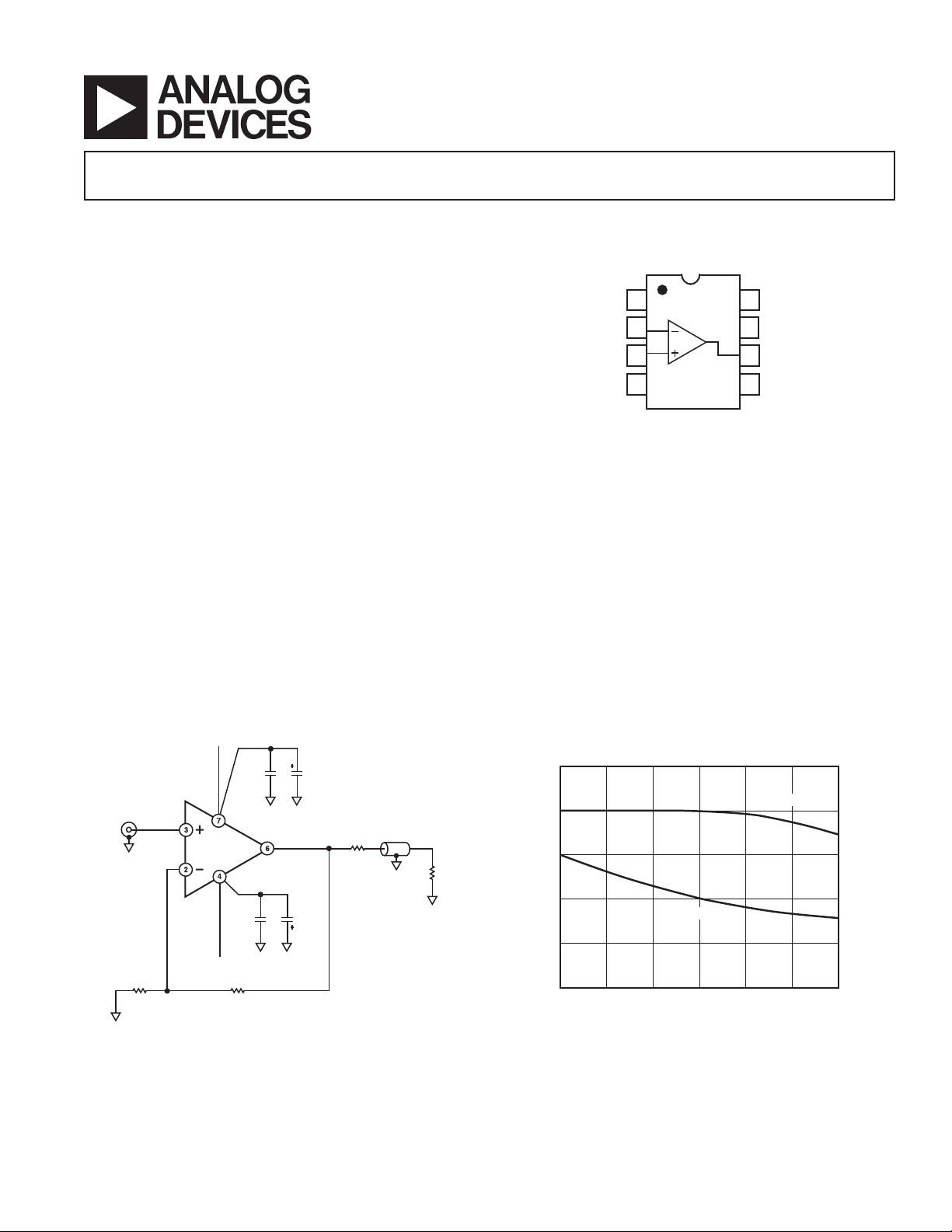
CONNECTION DIAGRAM
8-Lead Plastic Mini-DIP (N) and SOIC (R) Packages
NULL
–IN
+IN
–V
1
2
3
4
S
NC = NO CONNECT
AD818
TOP VIEW
8
7
6
5
NULL
+V
S
OUTPUT
NC
any video application. The 130 MHz 3 dB bandwidth (G = +2)
and 500 V/ms slew rate make the AD818 useful in many high speed
applications including video monitors, CATV, color copiers,
image scanners, and fax machines.
The AD818 is fully specified for operation with a single +5 V
power supply and with dual supplies from ±5 V to ±15 V. This
power supply flexibility, coupled with a very low supply current
of 7.5 mA and excellent ac characteristics under all power supply conditions, make the AD818 the ideal choice for many
demanding yet power sensitive applications.
The AD818 is a voltage feedback op amp and excels as a gain
stage in high speed and video systems (gain ≥ 2, or gain £ –1). It
achieves a settling time of 45 ns to 0.1%, with a low input offset
voltage of 2 mV max.
The AD818 is available in low cost, small 8-lead PDIP and
SOIC packages.
0.01F 2.2F
R
V
IN
AD818
0.1F
–15V
1k⍀
1k⍀
2.2F
75⍀
BT
75⍀
R
T
75⍀
Figure 1. Video Line Driver
REV. C
Information furnished by Analog Devices is believed to be accurate and
reliable. However, no responsibility is assumed by Analog Devices for its
use, nor for any infringements of patents or other rights of third parties that
may result from its use. No license is granted by implication or otherwise
under any patent or patent rights of Analog Devices. Trademarks and
registered trademarks are the property of their respective companies.
0.02
DIFF GAIN
0.06
0.05
0.04
0.03
DIFFERENTIAL PHASE (Degrees)
510
DIFF PHASE
SUPPLY VOLTAGE (ⴞV)
0.01
0.00
DIFFERENTIAL GAIN (%)
15
Figure 2. Differential Gain and Phase vs. Supply
One Technology Way, P.O. Box 9106, Norwood, MA 02062-9106, U.S.A.
Tel: 781/329-4700 www.analog.com
Fax: 781/326-8703 © 2003 Analog Devices, Inc. All rights reserved.

AD818–SPECIFICATIONS
(@ TA = 25ⴗC, unless otherwise noted.)
AD818A
Parameter Conditions V
S
Min Typ Max Unit
DYNAMIC PERFORMANCE
–3 dB Bandwidth Gain = +2 ±5 V 70 95 MHz
±15 V 100 130 MHz
0 V, +5 V 40 55 MHz
Gain = –1 ±5 V 50 70 MHz
±15 V 70 100 MHz
0 V, +5 V 30 50 MHz
Bandwidth for 0.1 dB Flatness Gain = +2 ±5 V 20 43 MHz
= 2 pF ± 15 V 40 55 MHz
C
C
0 V, +5 V 10 18 MHz
Gain = –1 ±5 V 18 34 MHz
= 2 pF ± 15 V 40 72 MHz
C
C
0 V, +5 V 10 19 MHz
Full Power Bandwidth* V
Slew Rate R
= 5 V p-p
OUT
R
= 500 W±5 V 25.5 MHz
LOAD
= 20 V p-p
V
OUT
R
= 1 kW±15 V 8.0 MHz
LOAD
= 1 kW±5 V 350 400 V/ms
LOAD
Gain = –1 ±15 V 450 500 V/ms
0 V, +5 V 250 300 V/ms
Settling Time to 0.1% –2.5 V to +2.5 V ±5 V 45 ns
0 V–10 V Step, A
= –1 ±15 V 45 ns
V
Settling Time to 0.01% –2.5 V to +2.5 V ±5 V 80 ns
= –1 ±15 V 80 ns
V
Total Harmonic Distortion F
0 V–10 V Step, A
= 1 MHz ±15 V 63 dB
C
Differential Gain Error NTSC ±15 V 0.005 0.01 %
= 150 W)Gain = +2 ±5 V 0.01 0.02 %
(R
L
0 V, +5 V 0.08 %
Differential Phase Error NTSC ±15 V 0.045 0.09 Degrees
= 150 W)Gain = +2 ±5 V 0.06 0.09 Degrees
(R
L
0 V, +5 V 0.1 Degrees
Cap Load Drive 10 pF
INPUT OFFSET VOLTAGE ±5 V to ± 15 V 0.5 2 mV
T
MIN
to T
MAX
3mV
Offset Drift 10 mV/∞C
INPUT BIAS CURRENT ±5 V, ± 15 V 3.3 6.6 mA
T
T
MIN
MAX
10 mA
4.4 mA
INPUT OFFSET CURRENT ±5 V, ± 15 V 25 300 nA
T
MIN
to T
MAX
500 nA
Offset Current Drift 0.3 nA/∞C
OPEN-LOOP GAIN V
= ±2.5 V ±5 V
OUT
R
= 500 W 35 V/mV
LOAD
to T
T
R
V
R
T
V
R
MIN
LOAD
OUT
LOAD
MIN
OUT
LOAD
MAX
= 150 W 24 V/mV
= ±10 V ±15 V
= 1 kW 69 V/mV
to T
MAX
= ±7.5 V ±15 V
= 150 W
2 V/mV
3 V/mV
(50 mA Output) 3 5 V/mV
COMMON-MODE REJECTION V
= ±2.5 V ±5 V 82 100 dB
CM
= ±12 V ±15 V 86 120 dB
V
CM
T
MIN
to T
MAX
±15 V 84 100 dB
REV. C–2–
AD818
AD818A
Parameter Conditions V
POWER SUPPLY REJECTION V
= ±5 V to ± 15 V 80 90 dB
S
T
to T
MIN
MAX
S
INPUT VOLTAGE NOISE f = 10 kHz ±5 V, ± 15 V 10 nV/÷Hz
INPUT CURRENT NOISE f = 10 kHz ±5 V, ± 15 V 1.5 pA/÷Hz
INPUT COMMON-MODE
VOLTAGE RANGE ±5 V +3.8 +4.3 V
±15 V +13 +14.3 V
0 V, +5 V +3.8 +4.3 V
OUTPUT VOLTAGE SWING R
= 500 W±5 V 3.3 3.8 ±V
LOAD
= 150 W±5 V 3.2 3.6 ±V
R
LOAD
R
= 1 kW±15 V 13.3 13.7 ±V
LOAD
R
= 500 W±15 V 12.8 13.4 ±V
LOAD
= 500 W 0 V, +5 V 1.5, 3.5 V
R
LOAD
Output Current ±15 V 50 mA
±5 V 50 mA
0 V, +5 V 30 mA
Short-Circuit Current ±15 V 90 mA
INPUT RESISTANCE 300 kW
INPUT CAPACITANCE 1.5 pF
OUTPUT RESISTANCE Open Loop 8 W
POWER SUPPLY
Operating Range Dual Supply ±2.5 ± 18 V
Single Supply +5 +36 V
Quiescent Current ±5 V 7.0 7.5 mA
T
MIN
to T
MAX
±5 V 7.5 mA
±15 V 7.5 mA
T
*Full power bandwidth = slew rate/(2p V
Specifications subject to change without notice.
PEAK
).
MIN
to T
MAX
±15 V 7.0 7.5 mA
Min Typ Max Unit
80 dB
–2.7 –3.4 V
–12 –13.4 V
+1.2 +0.9 V
REV. C
–3–
AD818
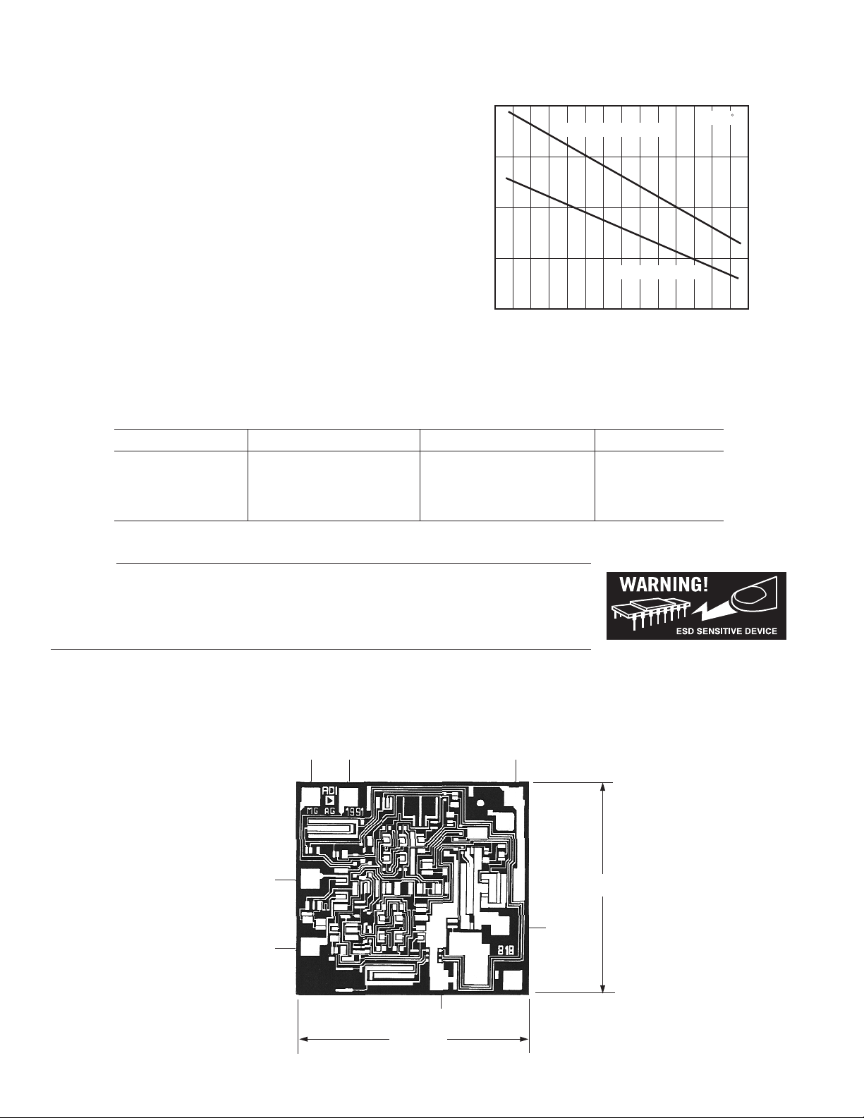
ABSOLUTE MAXIMUM RATINGS
Supply Voltage . . . . . . . . . . . . . . . . . . . . . . . . . . . . . . . . ±18 V
Internal Power Dissipation
2
1
Plastic (N) . . . . . . . . . . . . . . . . . . . . . . See Derating Curves
Small Outline (R) . . . . . . . . . . . . . . . . . See Derating Curves
Input Voltage (Common Mode) . . . . . . . . . . . . . . . . . . . . ±V
S
Differential Input Voltage . . . . . . . . . . . . . . . . . . . . . . . . ±6 V
Output Short-Circuit Duration . . . . . . . . See Derating Curves
Storage Temperature Range (N, R) . . . . . . . . –65∞C to +125∞C
Operating Temperature Range . . . . . . . . . . . .–40∞C to +85∞C
Lead Temperature Range (Soldering 10 sec) . . . . . . . . . 300∞C
NOTES
1
Stresses above those listed under Absolute Maximum Ratings may cause permanent damage to the device. This is a stress rating only; functional operation of the
device at these or any other conditions above those indicated in the operational
section of this specification is not implied. Exposure to absolute maximum rating
conditions for extended periods may affect device reliability.
2
Specification is for device in free air: 8-lead plastic package, JA = 90∞C/W; 8-lead
SOIC package, JA = 155∞C/W.
ORDERING GUIDE
Model Temperature Range Package Description Package Option
AD818AN –40∞C to +85∞C 8-Lead Plastic PDIP N-8
AD818AR –40∞C to +85∞C 8-Lead Plastic SOIC R-8
AD818AR-REEL –40∞C to +85∞C 13" Tape and Reel R-8
AD818AR-REEL7 –40∞C to +85∞C 7" Tape and Reel R-8
2.0
8-LEAD MINI-DIP PACKAGE
1.5
1.0
0.5
MAXIMUM POWER DISSIPATION (W)
0
–30
–50 90
AMBIENT TEMPERATURE (ⴗC)
8-LEAD SOIC PACKAGE
50 703010–10
TJ = 150 C
80–40 40 60200–20
Figure 3. Maximum Power Dissipation vs. Temperature
for Different Package Types
CAUTION
ESD (electrostatic discharge) sensitive device. Electrostatic charges as high as 4000 V readily
accumulate on the human body and test equipment and can discharge without detection. Although the
AD818 features proprietary ESD protection circuitry, permanent damage may occur on devices
subjected to high energy electrostatic discharges. Therefore, proper ESD precautions are recommended
to avoid performance degradation or loss of functionality.
METALLIZATION PHOTOGRAPH
Dimensions shown in inches and (mm)
OFFSET
–INPUT 2
+INPUT 3
OFFSET
NULL
1
NULL
8
+V
S
7
0.0523
(1.33)
6 OUTPUT
0.0559 (1.42)
4
–V
S
REV. C–4–
Typical Performance Characteristics–AD818
–40ⴗC
8.0
6.0
020
7.5
6.5
5
7.0
10
15
SUPPLY VOLTAGE (ⴞV)
QUIESCENT SUPPLY CURRENT (mA)
+25ⴗC
+85ⴗC
100
1
0.01
1k 10k 100M10M1M100k
0.1
10
FREQUENCY (Hz)
CLOSED-LOOP OUTPUT IMPEDANCE (⍀)
20
15
+V
CM
10
–V
CM
5
INPUT COMMON-MODE RANGE (ⴞV)
0
020
5
SUPPLY VOLTAGE (ⴞV)
10
15
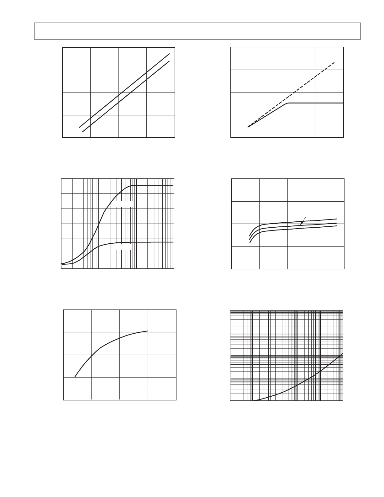
TPC 1. Common-Mode Voltage Range vs. Supply
30
25
20
15
VS = ⴞ15V
20
15
10
5
OUTPUT VOLTAGE SWING (ⴞV)
0
020
TPC 4. Output Voltage Swing vs. Supply
RL = 500
5
SUPPLY VOLTAGE (ⴞV)
10
RL = 150
⍀
⍀
15
10
OUTPUT VOLTAGE SWING (V p-p)
5
0
10 10k
TPC 2. Output Voltage Swing vs. Load Resistance
600
500
400
SLEW RATE (V/s)
300
200
020
5
TPC 3. Slew Rate vs. Supply Voltage
VS = ⴞ5V
LOAD RESISTANCE (⍀)
10
SUPPLY VOLTAGE (ⴞV)
1k100
TPC 5. Quiescent Supply Current vs. Supply Voltage
15
TPC 6. Closed-Loop Output Impedance vs. Frequency
REV. C
–5–

AD818
7
6
5
4
3
INPUT BIAS CURRENT (A)
2
1
–40
–60
TEMPERATURE (ⴗC)
TPC 7. Input Bias Current vs. Temperature
70
PHASE MARGINPHASE MARGIN
60
50
GAIN/BANDWIDTH
40
PHASE MARGIN (Degrees)
130
110
SOURCE CURRENT
90
SINK CURRENT
70
50
SHORT CIRCUIT CURRENT (mA)
140
120806040 100200–20
30
–40
–60
TEMPERATURE (ⴗC)
140
120100806040200–20
TPC 10. Short-Circuit Current vs. Temperature
95
85
75
–3dB BANDWIDTH (MHz)
65
100
80
60
40
20
OPEN-LOOP GAIN (dB)
0
ⴞ5V SUPPLIES
R
= 1k⍀
L
ⴞ15V SUPPLIES
= 1k⍀
R
L
PHASE ⴞ5V OR
ⴞ15V SUPPLIES
100
80
60
40
20
PHASE MARGIN (Degrees)
0
30
–60 140
–40
TEMPERATURE (ⴗC)
100 120806040200–20
55
TPC 8. –3 dB Bandwidth and Phase Margin vs.
Temperature, Gain = +2
9
8
7
6
5
OPEN-LOOP GAIN (V/mV)
4
3
100 1k 10k
LOAD RESISTANCE (⍀)
ⴞ15V
ⴞ5V
TPC 9. Open-Loop Gain vs. Load Resistance
–20
10k
1k
FREQUENCY (Hz)
100M10M1M100k
1G
TPC 11. Open-Loop Gain and Phase Margin vs.
Frequency
100
90
80
70
60
50
PSR (dB)
40
30
20
10
1k100
+SUPPLY
–SUPPLY
FREQUENCY (Hz)
100M
10M1M100k10k
TPC 12. Power Supply Rejection vs. Frequency
REV. C–6–

120
30
10
0
100k 1M 100M10M
20
OUTPUT VOLTAGE (V p-p)
FREQUENCY (Hz)
RL = 1k⍀
RL = 150⍀
–40
–100
10M
–70
–90
1k
–80
100
–50
–60
1M100k10k
FREQUENCY (Hz)
HARMONIC DISTORTION (dB)
SECOND HARMONIC
R
L
= 150⍀
2V p-p
THIRD HARMONIC
650
250
–60 140
550
350
–40
450
100 120806040200–20
TEMPERATURE (ⴗC)
SLEW RATE (V/s)
100
80
CMR (dB)
60
AD818
40
1k 10M
10k
100k
FREQUENCY (Hz)
1M
TPC 13. Common-Mode Rejection vs. Frequency
10
8
6
4
1%
–2
–4
–6
OUTPUT SWING FROM 0 TO ⴞV (V)
–8
–10
2
0
0.1%
1%
0.1%
20
0
0.01%
0.01%
SETTLING TIME (ns)
160
140120100806040
TPC 14. Output Swing and Error vs. Settling Time
50
TPC 16. Output Voltage vs. Frequency
TPC 17. Harmonic Distortion vs. Frequency
40
30
20
10
INPUT VOLTAGE NOISE (nV/ Hz)
REV. C
0
10
1
FREQUENCY (Hz)
TPC 15. Input Voltage Noise Spectral Density vs.
Frequency
10M
1M100k10k1k100
TPC 18. Slew Rate vs. Temperature
–7–

AD818
DIFF GAIN
0.02
0.01
C
F
1k⍀
+V
S
3.3F
0.06
0.05
DIFF PHASE
0.04
DIFFERENTIAL PHASE (Degrees)
0.03
510
SUPPLY VOLTAGE (ⴞV)
0.00
DIFFERENTIAL GAIN (%)
15
TPC 19. Differential Gain and Phase vs. Supply Voltage
C
1k
AD818
⍀
150
ⴞ
C
15V
V
OUT
⍀
0.1dB
10
C
V
ⴞ
9
ⴞ
+5V 1pF 18MHz
8
7
6
GAIN (dB)
5
4
3
2
1
1M 10M 100M 1G
FLATNESS
S
C
15V 2pF 55MHz
5V 1pF 43MHz
1k
V
ⴞ
5V
+5V
FREQUENCY (Hz)
⍀
IN
HP
PULSE (LS)
OR FUNCTION
(SS)
GENERATOR
100
0%
V
IN
1k⍀
50⍀
AD818
–V
0.01F
TEKTRONIX
P6201 FET
V
OUT
0.01F
3.3F
S
PROBE
R
L
TPC 22. Inverting Amplifier Connection
2V
50ns
90
10
2V
TEKTRONIX
7A24
PREAMP
TPC 20. Closed-Loop Gain vs. Frequency (G = +2)
10
0.1dB
8
FLATNESS
V
S
ⴞ15V 72MHz
6
ⴞ5V 34MHz
+5V 19MHz
4
2
0
GAIN (dB)
–2
–4
–6
–8
–10
1M 10M 100M 1G
+5V
FREQUENCY (Hz)
V
ⴞ5V
1k⍀
IN
2pF
1k⍀
AD818
150⍀
ⴞ15V
V
OUT
TPC 21. Closed-Loop Gain vs. Frequency (G = –1)
TPC 23. Inverter Large Signal Pulse Response;
VS = ±5 V, CF = 1 pF, RL = 1 k
200mV
100
90
10
0%
200mV
W
10ns
TPC 24. Inverter Small Signal Pulse Response;
= ±5 V, CF = 1 pF, RL = 150
V
S
W
REV. C–8–

AD818
C
F
5V
100
90
10
0%
50ns
5V
TPC 25. Inverter Large Signal Pulse Response;
= ±15 V, CF = 1 pF, RL = 1 k
V
S
200mV
100
90
W
10ns
1k⍀
+V
S
AD818
–V
S
3.3F
0.01F
V
0.01F
3.3F
OUT
HP
PULSE (LS)
OR FUNCTION
(SS)
GENERATOR
1k⍀
V
IN
100⍀
50⍀
TPC 28. Noninverting Amplifier Connection
1V
100
90
TEKTRONIX
P6201 FET
PROBE
R
L
50ns
TEKTRONIX
7A24
PREAMP
10
0%
200mV
TPC 26. Inverter Small Signal Pulse Response;
VS = ±15 V, CF = 1 pF, RL = 150
200mV
100
90
10
0%
200mV
W
10ns
TPC 27. Inverter Small Signal Pulse Response;
= ±5 V, CF = 0 pF, RL = 150
V
S
W
10
0%
2V
TPC 29. Noninverting Large Signal Pulse Response;
VS = ±5 V, CF = 1 pF, RL = 1 k
100mV
100
90
10
0%
200mV
W
10ns
TPC 30. Noninverting Small Signal Pulse
Response; V
= ±5 V, CF = 1 pF, RL = 150
S
W
REV. C
–9–

AD818
5V
100
90
10
0%
5V
50ns
TPC 31. Noninverting Large Signal Pulse Response;
V
= ±15 V, CF = 1 pF, RL = 1 k
S
100mV
100
90
W
10ns
100mV
100
90
10
0%
200mV
10ns
TPC 33. Noninverting Small Signal Pulse Response;
V
= ±5 V, CF = 0 pF, RL = 150
S
W
10
0%
200mV
TPC 32. Noninverting Small Signal Pulse Response;
VS = ±15 V, CF = 1 pF, RL = 150
W
REV. C–10–

+V
10k⍀
–V
S
VOS ADJUST
+V
S
AD818
R2
3.3k⍀
R1
3.3k⍀
R3
100⍀
C2
3.3F
V
IN
C1
0.01F
C4
0.001F
R4
1k⍀
AD818
V
OUT
V
S
3.3F
0.01F
SELECT C1, R1, R2
FOR DESIRED LOW
FREQUENCY CORNER.
C3
0.1F
R
L
150⍀
1k⍀
S
OUTPUT
–IN
+IN
–V
S
NULL 1
NULL 8
Figure 4. AD818 Simplified Schematic
THEORY OF OPERATION
The AD818 is a low cost video operational amplifier designed to
excel in high performance, high output current video applications.
The AD818 (Figure 4) consists of a degenerated NPN differential pair driving matched PNPs in a folded-cascode gain stage.
The output buffer stage employs emitter followers in a class
AB amplifier that delivers the necessary current to the load, while
maintaining low levels of distortion.
The AD818 will drive terminated cables and capacitive loads of
10 pF or less. As the closed-loop gain is increased, the AD818
will drive heavier capacitive loads without oscillating.
INPUT CONSIDERATIONS
An input protection resistor (RIN in TPC 28) is required in
circuits where the input to the AD818 will be subjected to transients of continuous overload voltages exceeding the ±6 V
maximum differential limit. This resistor provides protection for
the input transistors by limiting their maximum base current.
For high performance circuits, it is recommended that a “balancing” resistor be used to reduce the offset errors caused by
bias current flowing through the input and feedback resistors.
The balancing resistor equals the parallel combination of R
IN
and RF and thus provides a matched impedance at each input
terminal. The offset voltage error will then be reduced by more
than an order of magnitude.
AD818
may result in peaking. A small capacitance (1 pF–5 pF) may be
used in parallel with the feedback resistor to neutralize this effect.
Power supply leads should be bypassed to ground as close as
possible to the amplifier pins. Ceramic disc capacitors of 0.1 mF
are recommended.
Figure 5. Offset Null Configuration
OFFSET NULLING
The input offset voltage of the AD818 is inherently very low.
However, if additional nulling is required, the circuit shown
in Figure 5 can be used. The null range of the AD818 in this
configuration is ±10 mV.
SINGLE SUPPLY OPERATION
Another exciting feature of the AD818 is its ability to perform
well in a single supply configuration. The AD818 is ideally
suited for applications that require low power dissipation and
high output current.
Referring to Figure 6, careful consideration should be given to
the proper selection of component values. The choices for this
particular circuit are: R1 + R3储R2 combine with C1 to form a
low frequency corner of approximately 10 kHz. C4 was inserted
in series with R4 to maintain amplifier stability at high frequency.
Combining R3 with C2 forms a low-pass filter with a corner
frequency of approximately 500 Hz. This is needed to maintain
amplifier PSRR, since the supply is connected to V
the input divider. The values for R2 and C2 were chosen to
demonstrate the AD818’s exceptional output drive capability.
In this configuration, the output is centered around 2.5 V. In
order to eliminate the static dc current associated with this level,
C3 was inserted in series with R
.
L
through
IN
GROUNDING AND BYPASSING
When designing high frequency circuits, some special precautions
are in order. Circuits must be built with short interconnect leads.
When wiring components, care should be taken to provide a low
resistance, low inductance path to ground. Sockets should be
avoided, since their increased interlead capacitance can degrade
circuit bandwidth.
Feedback resistors should be of low enough value (£1 kW) to
ensure that the time constant formed with the inherent stray
capacitance at the amplifier’s summing junction will not limit
performance. This parasitic capacitance, along with the parallel
resistance of RF储RIN, forms a pole in the loop transmission, which
REV. C
Figure 6. Single-Supply Amplifier Configuration
–11–

AD818
ERROR AMPLIFIER
OUTPUT ⴛ 10
V
ERROR
2ⴛ
HP2835
DEVICE
UNDER
TEST
0.01F
0 TO ⴞ10V
POWER
SUPPLY
TTL LEVEL
SIGNAL
GENERATOR
50Hz
OUTPUT
DIGITAL
GROUND
ANALOG
GROUND
EI&S
DL1A05GM
MERCURY
RELAY
7, 8
1, 14
50⍀
COAX
CABLE
2.2F
500⍀
50⍀
ERROR
SIGNAL
OUTPUT
NULL
ADJUST
1k⍀
0.01F
100⍀
FALSE
SUMMING
NODE
500⍀
5pF–18pF
AD818
+V
S
1k⍀
2.2F
–V
S
Figure 7. Settling Time Test Circuit
AD818 SETTLING TIME
Settling time primarily comprises two regions. The first is the slew
time in which the amplifier is overdriven, where the output voltage
rate of change is at its maximum. The second is the linear time
period required for the amplifier to settle to within a specified
percentage of the final value.
Measuring the rapid settling time of the AD818 (45 ns to 0.1%
and 80 ns to 0.01%—10 V step) requires applying an input pulse
with a very fast edge and an extremely flat top. With the AD818
configured in a gain of –1, a clamped false summing junction
responds when the output error is within the sum of two diode
voltages (approximately 1 V). The signal is then amplified 20 times
by a clamped amplifier whose output is connected directly to a
sampling oscilloscope.
15pF
0.01F
100⍀
AD829
0.47F
+V
1.9k⍀
NOTE
USE CIRCUIT BOARD
WITH GROUND PLANE
10pF
SCOPE PROBE
CAPACITANCE
2ⴛ
HP2835
0.47F
0.01F
–V
S
S
TEKTRONIX P6201
FET PROBE TO
TEKTRONIX TYPE 11402
OSCILLOSCOPE
PREAMP INPUT SECTION
100⍀
1M⍀
SHORT, DIRECT CONNECTION
TO TEKTRONIX TYPE 11402
OSCILLOSCOPE PREAMP
INPUT SECTION
A High Performance Video Line Driver
The buffer circuit shown in Figure 8 will drive a back-terminated
75 W video line to standard video levels (1 V p-p) with 0.1 dB
gain flatness to 55 MHz with only 0.05∞ and 0.01% differential
phase and gain at the 3.58 MHz NTSC subcarrier frequency.
This level of performance, which meets the requirements for
high definition video displays and test equipment, is achieved
using only 7 mA quiescent current.
+15V
0.01F
V
IN
75⍀
R
T
1k⍀
AD818
1k⍀
–15V
0.01F
2.2F
2.2F
R
75⍀
BT
75⍀
R
T
75⍀
Figure 8. Video Line Driver
REV. C–12–

AD818
DIFFERENTIAL LINE RECEIVER
The differential receiver circuit of Figure 9 is useful for many
applications—from audio to video. It allows extraction of a low
level signal in the presence of common-mode noise, as shown in
Figure 10.
2pF
V
B
DIFFERENTIAL
INPUT
V
A
1k⍀
AD818
1k⍀
2pF
+5V
–5V
1k⍀
0.01F
0.01F
1k⍀
2.2F
V
OUT
2.2F
OUTPUT
Figure 9. Differential Line Receiver
200
100
90
V
A
V
1V
10n
s
20ns
A HIGH SPEED, 3-OP AMP IN AMP
The circuit of Figure 11 uses three high speed op amps: two
AD818s and an AD817. This high speed circuit lends itself well
to CCD imaging and other video speed applications. It has the
optional flexibility of both dc and ac trims for common-mode
rejection, plus the ability to adjust for minimum settling time.
2pF
EACH AMPLIFIER
+15V
10F
COMMON
10F
–15V
–V
IN
A1
AD818
1k⍀
5pF
R
G
5pF
1k⍀
A2
AD818
+V
IN
0.1F
0.1F
1k⍀
1k⍀
3pF
+V
S
1F
1F
–V
S
2pF–8pF
AD818
970⍀
50⍀
DC CMR
ADJUST
0.1F
0.1F
SETTLING
TIME AC
CMR ADJUST
1k⍀
A3
PIN 7
EACH
AMPLIFIER
PIN 4
EACH
AMPLIFIER
V
OUT
R
L
2k⍀
2V
10
0%
OUTPUT
200m
V
Figure 10. Performance of Line Receiver, RL = 150 W,
G = +2
BANDWIDTH, SETTLING TIME, AND TOTAL HARMONIC DISTORTION VS. GAIN
THD + NOISE
BELOW INPUT LEVEL
@ 10kHz
82dB
81dB
71dB
GAIN
3
10
100
R
G
1k⍀
222⍀
20⍀
CADJ
(pF)
2–8
2–8
2–8
SMALL
SIGNAL
BANDWIDTH
14.7MHz
4.5MHz
960kHz
SETTLING
TIME
TO 0.1%
200ns
370ns
2.5s
Figure 11. High Speed 3-Op Amp In Amp
REV. C
–13–

AD818
OUTLINE DIMENSIONS
8-Lead Plastic Dual In-Line Package [PDIP]
(N-8)
Dimensions shown in inches and (millimeters)
0.375 (9.53)
0.365 (9.27)
0.355 (9.02)
8
1
0.100 (2.54)
0.180
(4.57)
MAX
0.150 (3.81)
0.130 (3.30)
0.110 (2.79)
0.022 (0.56)
0.018 (0.46)
0.014 (0.36)
CONTROLLING DIMENSIONS ARE IN INCHES; MILLIMETER DIMENSIONS
(IN PARENTHESES) ARE ROUNDED-OFF INCH EQUIVALENTS FOR
REFERENCE ONLY AND ARE NOT APPROPRIATE FOR USE IN DESIGN
COMPLIANT TO JEDEC STANDARDS MO-095AA
BSC
5
4
0.295 (7.49)
0.285 (7.24)
0.275 (6.98)
0.015
(0.38)
MIN
SEATING
PLANE
0.060 (1.52)
0.050 (1.27)
0.045 (1.14)
0.325 (8.26)
0.310 (7.87)
0.300 (7.62)
0.150 (3.81)
0.135 (3.43)
0.120 (3.05)
0.015 (0.38)
0.010 (0.25)
0.008 (0.20)
8-Lead Standard Small Outline Package [SOIC]
(R-8)
Dimensions shown in millimeters and (inches)
5.00 (0.1968)
4.80 (0.1890)
4.00 (0.1574)
3.80 (0.1497)
0.25 (0.0098)
0.10 (0.0040)
COPLANARITY
0.10
CONTROLLING DIMENSIONS ARE IN MILLIMETERS; INCH DIMENSIONS
(IN PARENTHESES) ARE ROUNDED-OFF MILLIMETER EQUIVALENTS FOR
REFERENCE ONLY AND ARE NOT APPROPRIATE FOR USE IN DESIGN
85
1.27 (0.0500)
SEATING
PLANE
COMPLIANT TO JEDEC STANDARDS MS-012AA
BSC
6.20 (0.2440)
5.80 (0.2284)
41
1.75 (0.0688)
1.35 (0.0532)
0.51 (0.0201)
0.31 (0.0122)
0.25 (0.0098)
0.17 (0.0067)
0.50 (0.0196)
0.25 (0.0099)
8ⴗ
0ⴗ
1.27 (0.0500)
0.40 (0.0157)
ⴛ 45ⴗ
REV. C–14–

AD818
Revision History
Location Page
5/03—Data Sheet changed from REV. B to REV. C.
Renumbered Figures and TPCs . . . . . . . . . . . . . . . . . . . . . . . . . . . . . . . . . . . . . . . . . . . . . . . . . . . . . . . . . . . . . . . . . . . . . . .Universal
Changes to SPECIFICATIONS . . . . . . . . . . . . . . . . . . . . . . . . . . . . . . . . . . . . . . . . . . . . . . . . . . . . . . . . . . . . . . . . . . . . . . . . . . . . 2
Changes to ORDERING GUIDE . . . . . . . . . . . . . . . . . . . . . . . . . . . . . . . . . . . . . . . . . . . . . . . . . . . . . . . . . . . . . . . . . . . . . . . . . . . 4
Changes to Figures 9 and 10 . . . . . . . . . . . . . . . . . . . . . . . . . . . . . . . . . . . . . . . . . . . . . . . . . . . . . . . . . . . . . . . . . . . . . . . . . . . . . . 12
Updated OUTLINE DIMENSIONS . . . . . . . . . . . . . . . . . . . . . . . . . . . . . . . . . . . . . . . . . . . . . . . . . . . . . . . . . . . . . . . . . . . . . . . 14
REV. C
–15–

C00872–0–5/03(C)
–16–
 Loading...