High Speed, Low Power
a
FEATURES
Low Cost
High Speed
50 MHz Unity Gain Bandwidth
350 V/ms Slew Rate
45 ns Settling Time to 0.1% (10 V Step)
Flexible Power Supply
Specified for Single (+5 V) and
Dual (65 V to 615 V) Power Supplies
Low Power: 7.5 mA max Supply Current
High Output Drive Capability
Drives Unlimited Capacitive Load
50 mA Minimum Output Current
Excellent Video Performance
70 MHz 0.1 dB Bandwidth (Gain = +1)
0.04% & 0.088 Differential Gain & Phase Errors
@ 3.58 MHz
Available in 8-Pin SOIC and 8-Pin Plastic Mini-DIP
PRODUCT DESCRIPTION
The AD817 is a low cost, low power, single/dual supply, high
speed op amp which is ideally suited for a broad spectrum of
signal conditioning and data acquisition applications. This
breakthrough product also features high output current drive
capability and the ability to drive an unlimited capacitive load
while still maintaining excellent signal integrity.
The 50 MHz unity gain bandwidth, 350 V/µs slew rate and set-
tling time of 45 ns (0.1%) make possible the processing of high
speed signals common to video and imaging systems. Furthermore, professional video performance is attained by offering differential gain & phase errors of 0.04% & 0.08° @ 3.58 MHz
and 0.1 dB flatness to 70 MHz (gain = +1).
Wide Supply Range Amplifier
AD817
CONNECTION DIAGRAM
8-Pin Plastic Mini-DIP (N) and
SOIC (R) Packages
NULL
1
NULL
–IN
+IN
–V
S
AD817
2
3
4
TOP VIEW
NC = NO CONNECT
The AD817 is fully specified for operation with a single +5 V
power supply and with dual supplies from ± 5 V to ±15 V. This
power supply flexibility, coupled with a very low supply current
of 7.5 mA and excellent ac characteristics under all power supply conditions, make the AD817 the ideal choice for many demanding yet power sensitive applications.
In applications such as ADC buffers and line drivers the AD817
simplifies the design task with its unique combination of a
50 mA minimum output current and the ability to drive
unlimited capacitive loads.
The AD817 is available in 8-pin plastic mini-DIP and SOIC
packages.
ORDERING GUIDE
Temperature Package Package
Model Range Description Option
AD817AN –40°C to +85°C 8-Pin Plastic DIP N-8
AD817AR –40°C to +85°C 8-Pin Plastic SOIC R-8
8
7
6
5
+V
S
OUTPUT
NC
1kΩ
3.3µF
+V
S
0.01µF
HP
PUL SE
GENERATOR
1kΩ
V
IN
50Ω
2
3
7
AD817
4
–V
V
OUT
6
C
0.01µF
3.3µF
S
L
1000pF
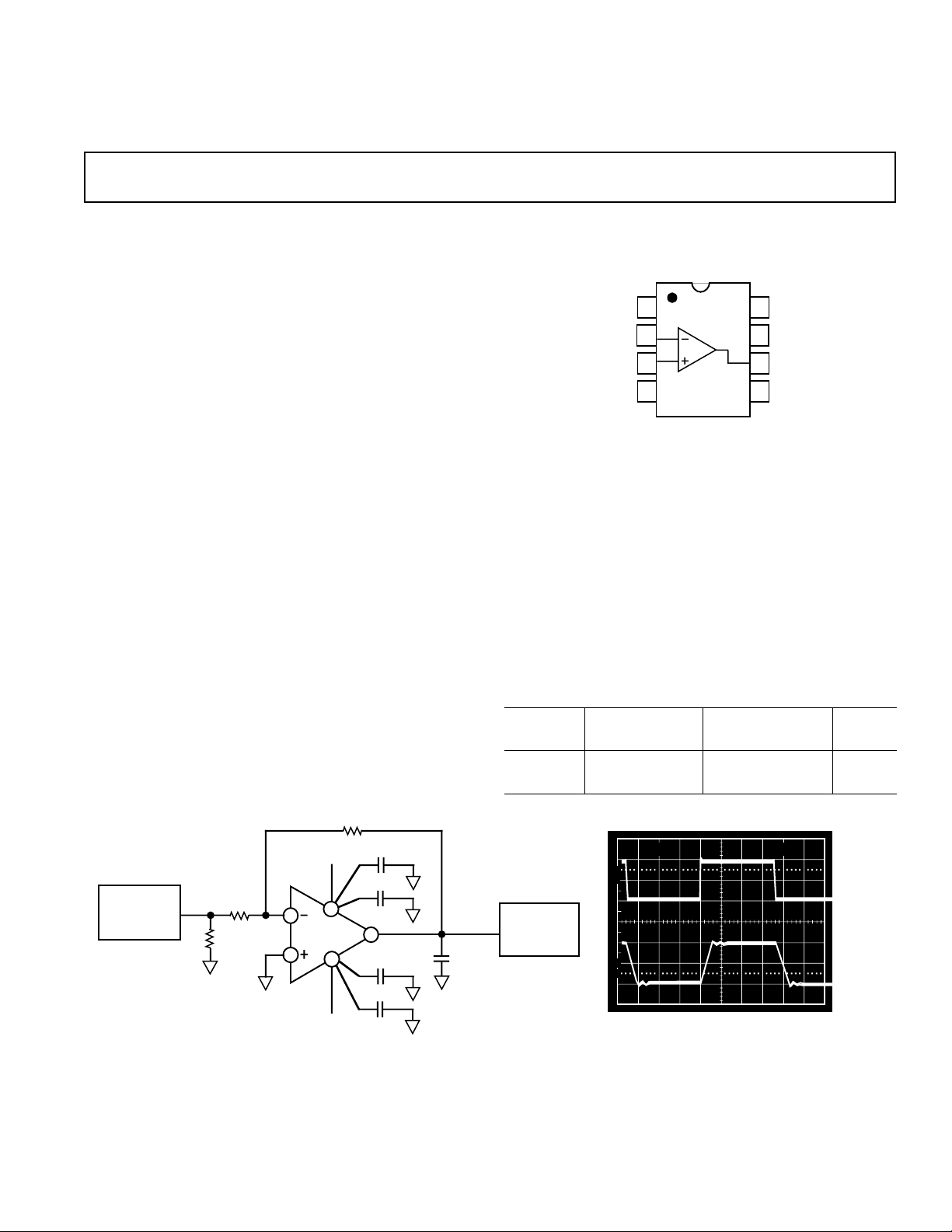
AD817 Driving a Large Capacitive Load
REV. B
Information furnished by Analog Devices is believed to be accurate and
reliable. However, no responsibility is assumed by Analog Devices for its
use, nor for any infringements of patents or other rights of third parties
which may result from its use. No license is granted by implication or
otherwise under any patent or patent rights of Analog Devices.
5V
100
90
TEKTRONIX
P6201 FET
PROBE
10
0%
One Technology Way, P.O. Box 9106, Norwood. MA 02062-9106, U.S.A.
Tel: 617/329-4700 Fax: 617/326-8703
500ns
100pF
LOAD
1000pF
LOAD
© Analog Devices, Inc., 1995

AD817–SPECIFICA TIONS
(@ TA = +258C, unless otherwise noted)
AD817A
Parameter Conditions V
S
Min Typ Max Units
DYNAMIC PERFORMANCE
Unity Gain Bandwidth ±5 V 30 35 MHz
±15 V 45 50 MHz
0, +5 V 25 29 MHz
Bandwidth for 0.1 dB Flatness Gain = +1 ±5 V 18 30 MHz
±15 V 40 70 MHz
Full Power Bandwidth
1
Slew Rate R
V
= 5 V p-p
OUT
R
= 500 Ω±5 V 15.9 MHz
LOAD
V
= 20 V p-p
OUT
R
= 1 kΩ±15 V 5.6 MHz
LOAD
= 1 kΩ±5 V 200 250 V/µs
LOAD
0, +5 V 10 20 MHz
Gain = 1 ±15 V 300 350 V/µs
0, +5 V 150 200 V/µs
Settling Time to 0.1% –2.5 V to +2.5 V ± 5 V 45 n s
0 V–10 V Step, A
= –1 ±15 V 45 ns
V
Settling Time to 0.01% –2.5 V to +2.5 V ± 5 V 70 ns
Total Harmonic Distortion F
0 V–10 V Step, A
= 1 MHz ±15 V 63 dB
C
= –1 ±15 V 70 ns
V
Differential Gain Error NTSC ±15 V 0.04 0.08 %
(R
= 150 Ω) Gain = +2 ±5 V 0.05 0.1 %
LOAD
0, +5 V 0.11 %
Differential Phase Error NTSC ±15 V 0.08 0.1 Degrees
(R
= 150 Ω) Gain = +2 ±5 V 0.06 0.1 Degrees
LOAD
0, +5 V 0.14 Degrees
INPUT OFFSET VOLTAGE ±5 V to ±15 V 0.5 2 mV
T
MIN
to T
MAX
3mV
Offset Drift 10 µV/°C
INPUT BIAS CURRENT ±5 V, ±15 V 3.3 6.6 µA
T
T
MIN
MAX
10 µA
4.4 µA
INPUT OFFSET CURRENT ±5 V, ±15 V 25 200 nA
T
MIN
to T
MAX
500 nA
Offset Current Drift 0.3 nA/°C
OPEN LOOP GAIN V
= ±2.5 V ±5 V
OUT
R
= 500 Ω 2 4 V/mV
LOAD
T
to T
R
V
R
T
V
R
MIN
LOAD
OUT
LOAD
MIN
OUT
LOAD
MAX
= 150 Ω 1.5 3 V/mV
= ±10 V ±15 V
= 1 kΩ 4 6 V/mV
to T
MAX
= ±7.5 V ±15 V
= 150 Ω
1.5 V/mV
2.5 5 V/mV
(50 mA Output) 2 4 V/mV
COMMON-MODE REJECTION V
= ±2.5 V ±5 78 100 dB
CM
V
= ±12 V ±15 V 86 120 dB
CM
±15 V 80 100 dB
POWER SUPPLY REJECTION VS = ±5 V to ±15 V 75 86 dB
T
MIN
to T
MAX
72 dB
INPUT VOLTAGE NOISE f = 10 kHz ±5 V, ±15 V 15 nV/√Hz
INPUT CURRENT NOISE f = 10 kHz ±5 V, ±15 V 1.5 pA/√Hz
–2–
REV. A

AD817
MAXIMUM POWER DISSIPATION – Watts
AMBIENT TEMPERATURE – °C
2.0
1.5
0
–50 90–40 –30 –20 –10 0 10 20 30 50 60 70 8040
1.0
0.5
8-PIN MINI-DIP PACKAGE
8-PIN SOIC PACKAGE
TJ = +150°C
WARNING!
ESD SENSITIVE DEVICE
AD817A
Parameter Conditions V
S
INPUT COMMON-MODE ±5 V +3.8 +4.3 V
VOLTAGE RANGE –2.7 –3.4 V
±15 V +13 +14.3 V
0, +5 V +3.8 +4.3 V
Min Typ Max Units
–12 –13.4 V
+1.2 +0.9 V
OUTPUT VOLTAGE SWING R
= 500 Ω±5 V 3.3 3.8 ±V
LOAD
R
= 150 Ω±5 V 3.2 3.6 ±V
LOAD
R
= 1 kΩ±15 V 13.3 13.7 ±V
LOAD
R
= 500 Ω±15 V 12.8 13.4 ±V
LOAD
R
= 500 Ω 0, +5 V +1.5,
LOAD
+3.5 V
Output Current ±15 V 50 mA
±5 V 50 mA
0, +5 V 30 mA
Short-Circuit Current ±15 V 90 mA
INPUT RESISTANCE 300 kΩ
INPUT CAPACITANCE 1.5 pF
OUTPUT RESISTANCE Open Loop 8 Ω
POWER SUPPLY
Operating Range Dual Supply ±2.5 ±18 V
Single Supply +5 +36 V
Quiescent Current ±5 V 7.0 7.5 mA
T
MIN
to T
MAX
±5 V 7.5 mA
±15 V 7.5 mA
T
to T
MIN
NOTES
1
Full power bandwidth = slew rate/2 π V
Specifications subject to change without notice.
ABSOLUTE MAXIMUM RATINGS
Supply Voltage . . . . . . . . . . . . . . . . . . . . . . . . . . . . . . . . ±18 V
Internal Power Dissipation
2
PEAK
.
1
MAX
±15 V 7.0 7.5 mA
Plastic (N) . . . . . . . . . . . . . . . . . . . . . . See Derating Curves
Small Outline (R) . . . . . . . . . . . . . . . . . See Derating Curves
Input Voltage (Common Mode) . . . . . . . . . . . . . . . . . . . . ±V
S
Differential Input Voltage . . . . . . . . . . . . . . . . . . . . . . . . ±6V
Output Short Circuit Duration . . . . . . . . See Derating Curves
Storage Temperature Range N, R . . . . . . . . .–65°C to +125°C
Operating Temperature Range . . . . . . . . . . . . –40°C to +85°C
Lead Temperature Range (Soldering 10 sec) . . . . . . . . +300°C
NOTES
1
Stresses above those listed under “Absolute Maximum Ratings” may cause
permanent damage to the device. This is a stress rating only and functional
operation of the device at these or any other conditions above those indicated in the
operational section of this specification is not implied. Exposure to absolute
maximum rating conditions for extended periods may affect device reliability.
2
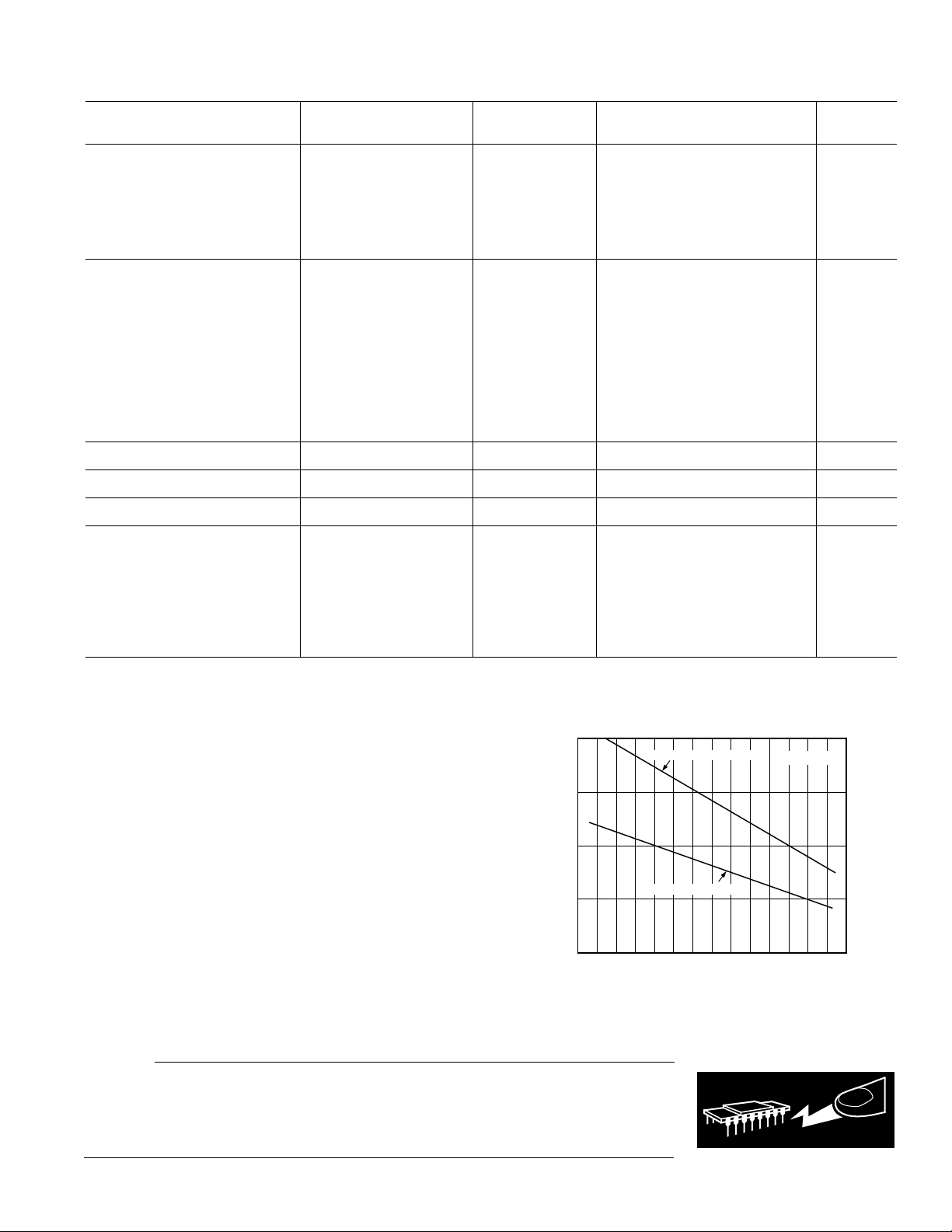
Specification is for device in free air: 8-pin plastic package: θJA = 100°C/watt;
8-pin SOIC package: θJA = 160°C/watt.
Maximum Power Dissipation vs. Temperature
CAUTION
ESD (electrostatic discharge) sensitive device. Electrostatic charges as high as 4000 V readily
accumulate on the human body and test equipment and can discharge without detection.
Although the AD817 features proprietary ESD protection circuitry, permanent damage may
occur on devices subjected to high energy electrostatic discharges. Therefore, proper ESD
precautions are recommended to avoid performance degradation or loss of functionality.
REV. B
–3–

AD817–Typical Characteristics
-40°C
8.0
6.0
7.5
6.5
7.0
02051015
SUPPLY VOLTAGE – ±Volts
QUIESCENT SUPPLY CURRENT – mA
+25°C
+85°C
SLEW RATE – V/µs
20501510
SUPPLY VOLTAGE – ±Volts
200
300
350
400
250
20
15
+V
CM
10
–V
CM
5
INPUT COMMON-MODE RANGE – ± Volts
0
02051015
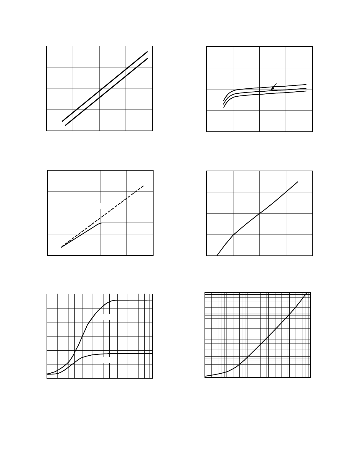
Figure 1. Common-Mode Voltage Range vs. Supply
20
15
SUPPLY VOLTAGE – ± Volts
Figure 4. Quiescent Supply Current vs. Supply Voltage
for Various Temperatures
10
5
OUTPUT VOLTAGE SWING – ±Volts
0
02051015
Figure 2. Output Voltage Swing vs. Supply
30
25
20
15
10
5
OUTPUT VOLTAGE SWING – Volts p-p
0
Figure 3. Output Voltage Swing vs. Load Resistance
RL = 500Ω
R
= 150Ω
L
SUPPLY VOLTAGE – ±Volts
VS = ±15V
VS = ±5V
LOAD RESISTANCE – Ω
Figure 5. Slew Rate vs. Supply Voltage
100
10
1
0.1
CLOSED-LOOP OUTPUT IMPEDANCE – Ohms
0.01
10k10010 1k
1k 10k 100M10M1M100k
FREQUENCY – Hz
Figure 6. Closed-Loop Output Impedance vs. Frequency
REV. B–4–
 Loading...