ANALOG DEVICES AD8158 Service Manual
O
O
6.5 Gbps
FEATURES
Quad 2:1 mux/1:2 demux
Optimized for dc to 6.5 Gbps NRZ data
Per-lane P/N pair inversion for routing ease
Programmable input equalization
Compensates up to 40 inches of FR4
Loss-of-signal detection
Programmable output pre-emphasis up to 12 dB
Programmable output levels with squelch and disable
Accepts ac-coupled or dc-coupled differential CML inputs
50 Ω on-chip termination
1:2 demux supports unicast or bicast operation
Port-level loopback
Port or single lane switching
1.8 V to 3.3 V flexible core supply
User-settable I/O supply from V
Low power, typically 2.0 W in basic configuration
100-lead LFCSP
−40°C to +85°C operating temperature range
APPLICATIONS
Low cost redundancy switch
SONET OC48/SDH16 and lower data rates
XAUI/GbE/FC/Infiniband over backplane
OIF CEI 6.25 Gbps over backplane
Serial data-level shift
4-/8-/12-lane equalizers or redrivers
to 1.2 V
CC
Ix_A[3:0]
Ix_B[3:0]
x_A[3:0]
x_B[3:0]
I2C_A0
I2C_A1
I2C_A2
SCL
SDA
Quad Buffer Mux/Demux
AD8158
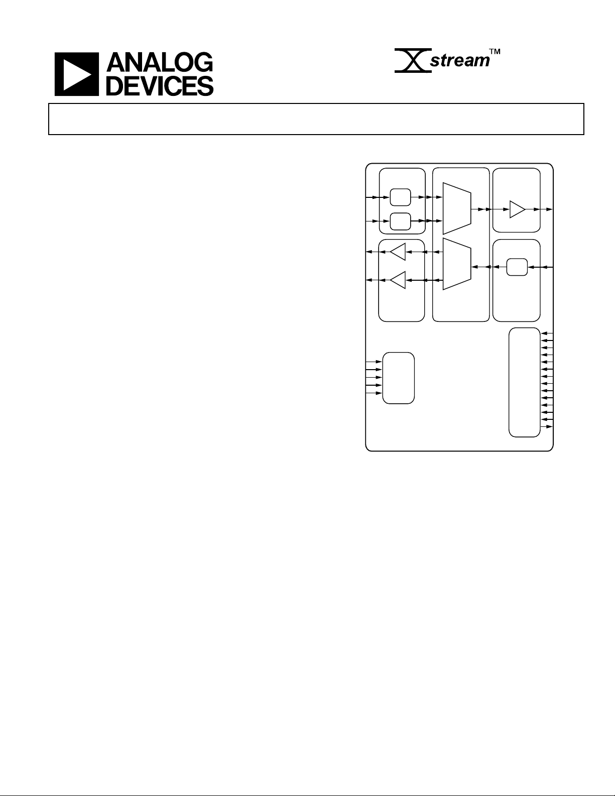
FUNCTIONAL BLOCK DIAGRAM
TRANSMIT
RECEIVE
EQUALIZATION
EQ
EQ
TRANSMIT
PRE-
EMPHASIS
I2C
CONTROL
LOGIC
AD8158
2:1
1:2
QUAD
2:1
MULTIPLEXER/
1:2
DEMULTIPLEXER
Figure 1.
PRE-
EMPHASIS
EQ
RECEIVE
EQUALIZATION
TOGGLE
CONTROL
LOGIC
Ox_C[3:0]
Ix_C[3:0]
LB_A
LB_B
LB_C
PE_A
PE_B
PE_C
EQ_A[1:0]
EQ_B[1:0]
EQ_C[1:0]
SEL[3:0]
BICAST
SEL4G
RESETb
LOS_INT
06646-001
GENERAL DESCRIPTION
The AD8158 is an asynchronous, protocol-agnostic, quad-lane
2:1 switch with a total of 12 differential CML inputs and
12 differential CML outputs. The signal path supports NRZ
signaling with data rates up to 6.5 Gbps per lane. Each lane
offers programmable receive equalization, programmable
output pre-emphasis, programmable output levels, and loss-ofsignal detection.
The nonblocking switch-core of the AD8158 implements a
2:1 multiplexer and 1:2 demultiplexer per lane and supports
independent lane switching through the four select pins,
SEL[3:0]. Each port is a four-lane link. Every lane implements
an asynchronous path supporting dc to 6.5 Gbps NRZ data,
fully independent of other lanes. The AD8158 has low latency
and very low lane-to-lane skew.
Rev. B
Information furnished by Analog Devices is believed to be accurate and reliable. However, no
responsibility is assumed by Analog Devices for its use, nor for any infringements of patents or other
rights of third parties that may result from its use. Specifications subject to change without notice. No
license is granted by implication or otherwise under any patent or patent rights of Analog Devices.
Trademarks and registered trademarks are the property of their respective owners.
The main application of the AD8158 is to support redundancy
on both the backplane and the line interface sides of a serial
link. The demultiplexing path implements unicast and bicast
capability, allowing the part to support either 1 + 1 or 1:1
redundancy.
The AD8158 is also suited for testing high speed serial links
because of its ability to duplicate incoming data. In a portmonitoring application, the AD8158 can maintain linkconnectivity with a pass-through connection from Port C to
Port A while sending a duplicate copy of the data to test
equipment on Port B.
The rich feature set of the AD8158 can be controlled either
through external toggle pins or by setting on-chip control
registers through the I
One Technology Way, P.O. Box 9106, Norwood, MA 02062-9106, U.S.A.
Tel: 781.329.4700 www.analog.com
Fax: 781.461.3113 ©2008–2009 Analog Devices, Inc. All rights reserved.
2
C interface.

AD8158
TABLE OF CONTENTS
Features .............................................................................................. 1
AD8158 Power Consumption .................................................. 23
Applications ....................................................................................... 1
Functional Block Diagram .............................................................. 1
General Description ......................................................................... 1
Revision History ............................................................................... 2
Specifications ..................................................................................... 3
I2C Timing Specifications ............................................................ 5
Absolute Maximum Ratings ............................................................ 6
ESD Caution .................................................................................. 6
Pin Configuration and Function Descriptions ............................. 7
Typical Performance Characteristics ........................................... 10
Theory of Operation ...................................................................... 16
The Switch (Mux/Demux/Unicast/Bicast/Loopback) ........... 17
Receivers ...................................................................................... 19
Loss of Signal (LOS) ................................................................... 21
Transmitters ................................................................................ 22
I2C Control Interface ...................................................................... 25
Serial Interface General Functionality..................................... 25
I2C Interface Data Transfers: Data Write ................................ 25
I2C Interface Data Transfers: Data Read ................................. 26
Applications Information .............................................................. 27
Output Compliance ................................................................... 28
Signal Levels and Common-Mode Shift for AC-Coupled and
DC-Coupled Outputs ................................................................ 29
Supply Sequencing ..................................................................... 31
Reset ............................................................................................. 31
Single Supply vs. Multiple Supply Operation ......................... 31
Printed Circuit Board (PCB) Layout Guidelines ................... 32
Register Map ................................................................................... 34
Outline Dimensions ....................................................................... 36
Ordering Guide .......................................................................... 36
REVISION HISTORY
12/09—Rev. A: Rev. B
Changes to LOS to Output Squelch Parameter (Table 1) ............ 3
Added Endnote 1 to Table 2 ............................................................ 5
Added Speed Select (SEL4G) to Table 6 ...................................... 17
Changes to Loss of Signal (LOS) section ..................................... 21
Deleted Table 15 .............................................................................. 21
Changes to Serial Interface General Functionality Section ...... 25
Added Reset Section ....................................................................... 31
Changes to Table 22 ........................................................................ 34
9/09—Rev. 0: Rev. A
Reorganized Layout ............................................................ Universal
Changes to Specifications Section .................................................. 3
Changes to Table 2 ............................................................................ 5
Changes to Table 3 ............................................................................ 6
Changes to Table 4 ............................................................................ 7
Changes to Theory of Operation Section .................................... 16
Added Table 15; Renumbered Sequentially ................................ 21
Changes to Applications Information Section ............................ 27
Changes to Table 23 ........................................................................ 34
6/08—Revision 0: Initial Version
Rev. B | Page 2 of 36

AD8158
SPECIFICATIONS
VCC = V
inputs and outputs, differential input swing = 800 mV p-p, T
Table 1.
Parameter Conditions Min Typ Max Unit
DYNAMIC PERFORMANCE
Data Rate/Channel (NRZ) DC 6.5 Gbps
Deterministic Jitter (No
Random Jitter (No Channel) RMS, data rate = 6.5 Gbps 1 ps
Residual Deterministic Jitter
Residual Deterministic Jitter
Propagation Delay 50% input to 50% output (maximum EQ) 700 ps
Lane-to-Lane Skew
Switching Time 50% logic switching to 50% output data 150 ns
Output Rise/Fall Time 20% to 80% (PE = lowest setting) 62 ps
INPUT CHARACTERISTICS
Differential Input Voltage
Input Voltage Range Single-ended absolute voltage level, VL minimum VEE + 0.6 V
Single-ended absolute voltage level, VH maximum VCC + 0.3 V
OUTPUT CHARACTERISTICS
Output Voltage Swing Differential, PE = 0, default output level, @ dc 590 725 820
Output Voltage Range, Single-
TX_HEADROOM = 0, VH maximum VCC + 0.6 V
TX_HEADROOM = 1, VL minimum VCC − 1.3 V
TX_HEADROOM = 1, VH maximum VCC + 0.6 V
Output Current Port A/B/C, PE_A/B/C = minimum 16 mA
Port A/B/C, PE_A/B/C = 6 dB, VOD = 800 mV p-p 32 mA
TERMINATION CHARACTERISTICS
Resistance Differential, VCC = V
LOS CHARACTERISTICS
DC Assert Level 50
DC Deassert Level 300
LOS to Output Squelch
LOS to Output Enable
POWER SUPPLY
Operating Range
= V
TTI
= 1.8 V, DVCC = 3.3 V, VEE = 0 V, RL = 50 Ω, basic configuration1, data rate = 6.5 Gbps, data pattern = PRBS7, ac-coupled
TTO
= 25°C, unless otherwise noted.
A
Data rate = 6.5 Gbps, EQ setting = 0 22 ps p-p
Channel)
Data rate 6.5 Gbps, 20 inch FR4 30 ps p-p
with Receive Equalization
Data rate 6.5 Gbps, 40 inch FR4 40 ps p-p
Data rate 6.5 Gbps, 10 inch FR4 35 ps p-p
with Transmit Preemphasis
Data rate 6.5 Gbps, 30 inch FR4 42 ps p-p
Signal path and switch architecture is balanced
90 ps
and symmetric (maximum EQ)
Swing
2
V
= VCC − 0.6 V, VCC = V
ICM
MIN
LOS control register = 0x05
TX_HEADROOM = 0, V
minimum VCC − 1.1 V
L
to V
MAX
, TA = T
MIN
to T
200 2000
,
MAX
Ended Absolute Voltage Level
to V
MAX
, TA = T
LOS_FILT = 0, V
V
= 1.8 V
CC
MIN
= 0 to 50% OP/ON settling,
ID
LOS_FILT = 0, data present to first valid transition,
= 1.8 V
V
CC
V
CC
VEE = 0 V, TX_HEADROOM = 0 1.6 1.8 to 3.3 3.6 V
VEE = 0 V, TX_HEADROOM = 1 2.2 3.3 3.6 V
MIN
to T
90 100 110 Ω
MAX
21 ns
67 ns
DVCC DVCC ≥ VCC, VEE = 0 V 1.6 1.8 to 3.3 3.6 V
V
1.2 VCC + 0.3 V
TTI
V
1.2 VCC + 0.3 V
TTO
mV p-p
diff
mV p-p
diff
mV p-p
diff
mV p-p
diff
Rev. B | Page 3 of 36

AD8158
Parameter Conditions Min Typ Max Unit
Supply Current
ICC
VCC = 1.8 V LB_x = 0, PE = 0 dB on all ports, default 370 450 mA
LB_x = 1, PE = 6 dB on all ports, default 730 850 mA
VCC = 3.3 V LB_x = 0, PE = 0 dB on all ports, default 400 460 mA
LB_x = 1, PE = 6 dB on all ports, default 780 860 mA
I
TTO
V
= 1.8 V LB_x = 0, PE = 0 dB on all ports, default 128 150 mA
TTO
LB_x = 1, PE = 6 dB on all ports, default 367 420 mA
V
= 3.3 V LB_x = 0, PE = 0 dB on all ports, default 134 152 mA
TTO
LB_x = 1, PE = 6 dB on all ports, default 388 422 mA
I
10 20 mA
TTI
I
2 4 mA
DVCC
THERMAL CHARACTERISTICS
Operating Temperature Range −40 +85 °C
θJA
θJC Still air; thermal resistance through exposed pad 1.4 °C/W
Maximum Junction Temperature 125 °C
LOGIC CHARACTERISTICS3 I
Input High (VIH) DV
Input Low (VIL) DV
Input High (VIH) DV
Input Low (VIL) DV
Output High (VOH) 2 kΩ pull-up resistor to DVCC DVCC V
Output Low (VOL) IOL = +3 mA VEE 0.4 V
1
Bicast is off, loopback is off on all ports, preemphasis is set to minimum on all ports, and equalization is set to minimum on all ports.
2
V
is the input common-mode voltage.
ICM
3
EQ control pins (EQ_A[1:0], EQ_B[1:0], EQ_C[1:0]) require 5 kΩ in series when DVCC > VCC.
Still air; JEDEC 4-layer test board, exposed pad
22.2 °C/W
soldered
2
C, SDA, SCL, control pins
= 3.3 V 0.7 × DVCC DVCC V
CC
= 3.3 V VEE 0.3 × DVCC V
CC
= 1.8 V 0.8 × DVCC DVCC V
CC
= 1.8 V VEE 0.2 × DVCC V
CC
Rev. B | Page 4 of 36
AD8158
A
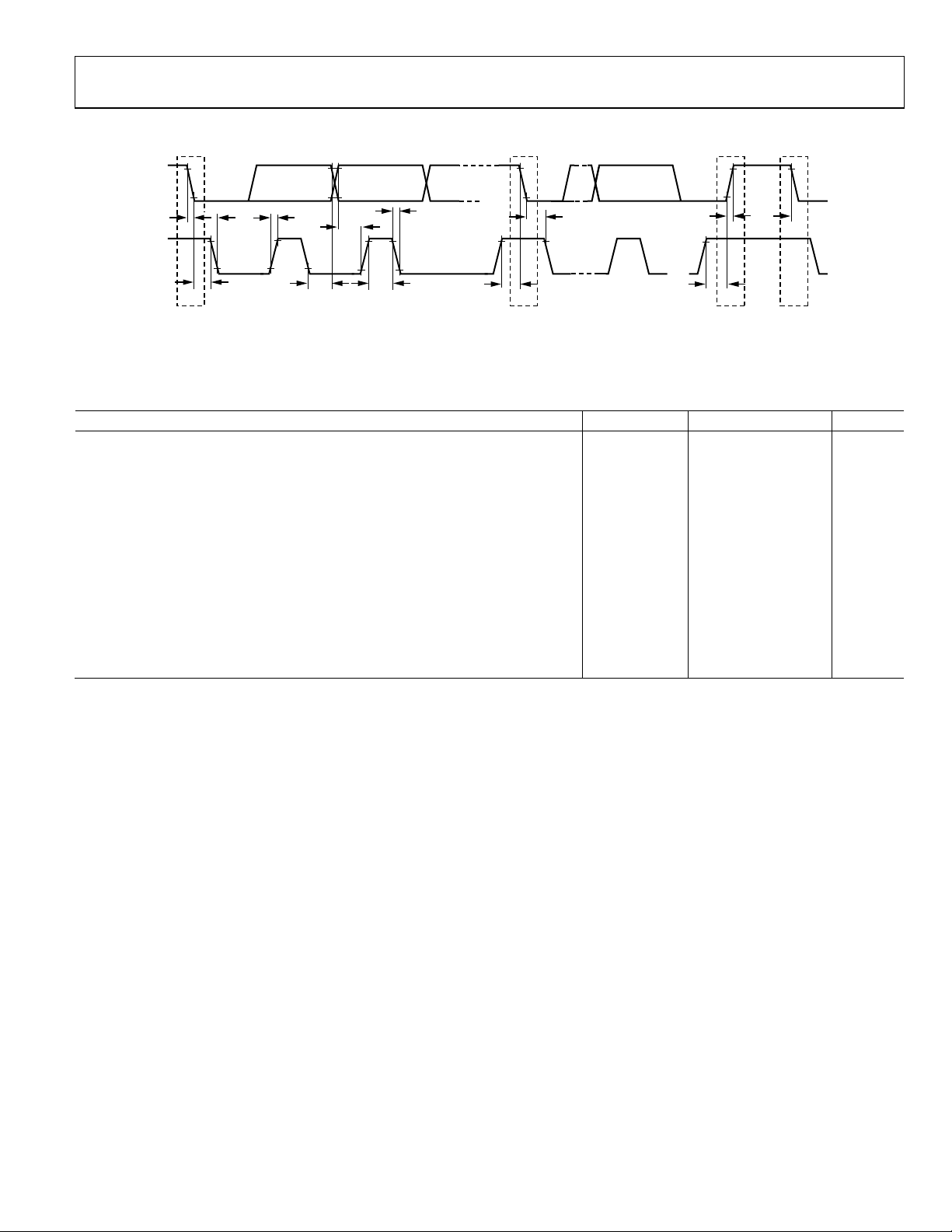
I2C TIMING SPECIFICATIONS
SD
t
t
F
SCL
NOTES
1. S = START CONDITION.
2. Sr = REPEAT START.
3. P = ST OP.
t
LOW
t
HD;STA
S Sr
t
R
t
HD;DAT
t
SU;DAT
t
HIGH
F
t
SU;STA
Figure 2. I
2
C Timing Diagram
t
HD;STA
Table 2. I2C Timing Parameters
Parameter Symbol Min Max Unit
SCL Clock Frequency f
Hold Time for a Start Condition t
Setup Time for a Repeated Start Condition t
Low Period of the SCL Clock t
High Period of the SCL Clock t
Data Hold Time t
Data Setup Time t
Rise Time for Both SDA and SCL t
Fall Time for Both SDA and SCL t
Setup Time for Stop Condition t
Bus Free Time Between a Stop and a Start Condition t
0 400+ kHz
SCL
HD;STA
SU;STA
LOW
HIGH
HD;DAT
SU;DAT
R
F
SU;STO
BUF
Bus Free Time After a Reset 1 μs
Reset Pulse Width1 10 ns
1
Reset pulse width is defined as the time RESETB is held below the logic low threshold (VIL) listed in Table 1 while the DVCC supply is within the operating range in Table 1.
t
SU;STO
t
R
t
BUF
SP
0.6 μs
0.6 μs
1.3 μs
0.6 μs
0 μs
10 ns
1 300 ns
1 300 ns
0.6 μs
1 μs
06646-102
Rev. B | Page 5 of 36
AD8158
ABSOLUTE MAXIMUM RATINGS
Table 3.
Parameter Rating
VCC to VEE 3.7 V
DVCC to VEE 3.7 V
V
Lower of (VCC + 0.6 V) or 3.6 V
TTI
V
Lower of (VCC + 0.6 V) or 3.6 V
TTO
VCC to DVCC 0.6 V
Internal Power Dissipation
Differential Input Voltage 2.0 V
Logic Input Voltage VEE − 0.3 V < VIN < VCC + 0.6 V
Storage Temperature Range
Junction Temperature
4.26 W
−65°C to +125°C
125°C
Stresses above those listed under Absolute Maximum Ratings
may cause permanent damage to the device. This is a stress
rating only; functional operation of the device at these or any
other conditions above those indicated in the operational
section of this specification is not implied. Exposure to absolute
maximum rating conditions for extended periods may affect
device reliability.
ESD CAUTION
Rev. B | Page 6 of 36
AD8158
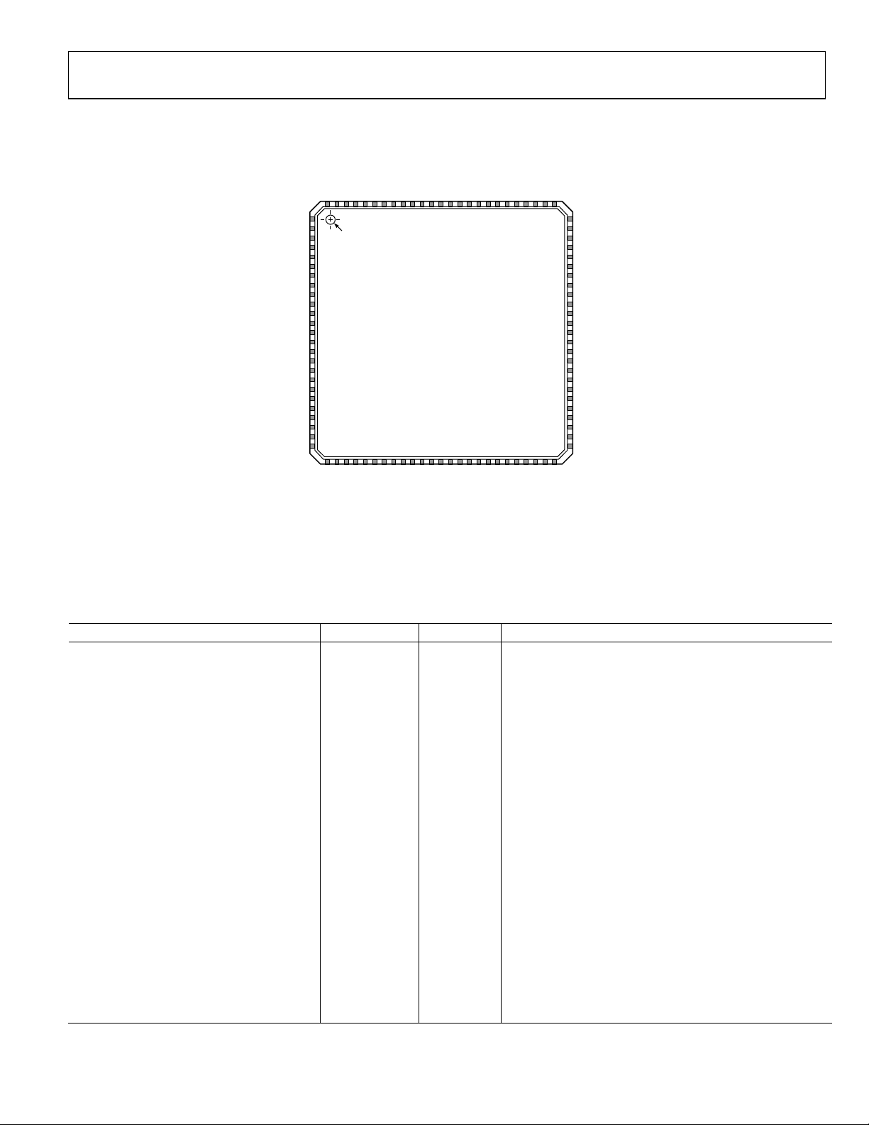
PIN CONFIGURATION AND FUNCTION DESCRIPTIONS
CC
TTI
IP_C1
IN_C1
V
IP_C2
IN_C2
VCCIP_C3
IN_C3
PE_A
PE_B
PE_C
LOS_INT
LB_A
LB_B
IP_C0
IN_C0
V
9392919089888786858483828180797877
94 VEE95 SEL3
96 SEL2
97 SEL1
98 SEL0
99 BICAST
100 SEL4G
V
EE
ON_A3
OP_A3
V
CC
ON_A2
OP_A2
V
TTO
ON_A1
OP_A1
10
V
CC
11
ON_A0
12
OP_A0
13
V
EE
14
IN_A3
15
IP_A3
16
V
CC
17IN_A2
18IP_A2
19V
TTI
20IN_A1
21IP_A1
22V
CC
23IN_A0
24IP_A0
25V
EE
NOTES
1. THE ePAD O N THE BOTTOM OF T HE P ACKAG E MUST BE EL E CTRICALLY CONNECTED TO V
CONTROL PORT C INPUTS
1
2
3
4
5
6
7
8
9
PIN 1
INDICATOR
PORT A OU TP UTSPORT A INPUTS
DIE IS PACKAGE D DIE UP
I2C PORT B OUTPUTS CONTROL
262728293031323334353637383941
CC
SCL
SDA
DV
I2C_A0
I2C_A1
I2C_A2
OP_B3
ON_B3
RESETb
AD8158
TOP VIEW
(Not to S cale)
CC
TTO
V
V
OP_B2
ON_B2
ON_B1
CONTROL
40OP_B1
43OP_B0
44V
42
45EQ_A0
EE
CC
V
ON_B0
Figure 3. Pin Configuration
LB_C
76
75 V
EE
74 OP_C0
73 ON_C0
72 V
CC
71 OP_C1
70 ON_C1
69 V
TTO
OP_C2
68
PORT C OU TP UTSPORT B INPUTS
67
ON_C2
66
V
CC
65
OP_C3
64
ON_C3
63
V
CC
62
IP_B0
61
IN_B0
60
V
CC
59
IP_B1
58
IN_B1
57
V
TTI
56
IP_B2
55
IN_B2
54
V
CC
53
IP_B3
52
IN_B3
51
V
EE
46EQ_A1
47EQ_B0
48EQ_B1
49EQ_C0
50EQ_C1
.
06646-002
EE
Table 4. Pin Function Descriptions
Pin No. Mnemonic Type Description
1, 13, 25, 44, 51, 75, 94, ePAD VEE Power Negative Supply
2 ON_A3 Output High Speed Output Complement
3 OP_A3 Output High Speed Output
4, 10, 16, 22, 35, 41, 54, 60, 63, 66, 72, 85, 91 VCC Power Positive Supply
5 ON_A2 Output High Speed Output Complement
6 OP_A2 Output High Speed Output
7, 38, 69 V
Power Port A, Port B, and Port C Output Termination Supply
TTO
8 ON_A1 Output High Speed Output Complement
9 OP_A1 Output High Speed Output
11 ON_A0 Output High Speed Output Complement
12 OP_A0 Output High Speed Output
14 IN_A3 Input High Speed Input Complement
15 IP_A3 Input High Speed Input
17 IN_A2 Input High Speed Input Complement
18 IP_A2 Input High Speed Input
19, 57, 88 V
Power Port A, Port B, and Port C Input Termination Supply
TTI
20 IN_A1 Input High Speed Input Complement
21 IP_A1 Input High Speed Input
23 IN_A0 Input High Speed Input Complement
24 IP_A0 Input High Speed Input
26 DVCC Power Digital Power Supply
Rev. B | Page 7 of 36
AD8158
Pin No. Mnemonic Type Description
27 SCL I2C I2C Clock Pin
28 SDA I2C I2C Data Pin
29 I2C_A0 I2C I2C Address Pin (LSB)
30 I2C_A1 I2C I2C Address Pin
31 I2C_A2 I2C I2C Address Pin (MSB)
32 RESETb Control1 Chip Reset. Active Low
33 ON_B3 Output High Speed Output Complement
34 OP_B3 Output High Speed Output
36 ON_B2 Output High Speed Output Complement
37 OP_B2 Output High Speed Output
39 ON_B1 Output High Speed Output Complement
40 OP_B1 Output High Speed Output
42 ON_B0 Output High Speed Output Complement
43 OP_B0 Output High Speed Output
45 EQ_A02 Control1 Port A Equalizer Control Bit 0 (LSB)
46 EQ_A12 Control1 Port A Equalizer Control Bit 1 (MSB)
47 EQ_B02 Control1 Port B Equalizer Control Bit 0 (LSB)
48 EQ_B12 Control1 Port B Equalizer Control Bit 1 (MSB)
49 EQ_C02 Control1 Port C Equalizer Control Bit 0 (LSB)
50 EQ_C12 Control1 Port C Equalizer Control Bit 1 (MSB)
52 IN_B3 Input High Speed Input Complement
53 IP_B3 Input High Speed Input
55 IN_B2 Input High Speed Input Complement
56 IP_B2 Input High Speed Input
58 IN_B1 Input High Speed Input Complement
59 IP_B1 Input High Speed Input
61 IN_B0 Input High Speed Input Complement
62 IP_B0 Input High Speed Input
64 ON_C3 Output High Speed Output Complement
65 OP_C3 Output High Speed Output
67 ON_C2 Output High Speed Output Complement
68 OP_C2 Output High Speed Output
70 ON_C1 Output High Speed Output Complement
71 OP_C1 Output High Speed Output
73 ON_C0 Output High Speed Output Complement
74 OP_C0 Output High Speed Output
76 LB_C Control1 Loopback Enable for Port C, Active High
77 LB_B Control1 Loopback Enable for Port B, Active High
78 LB_A Control1 Loopback Enable for Port A, Active High
79 LOS_INT Interrupt1 Loss of Signal Interrupt, Active High
80 PE_C Control1 Pre-Emphasis Control for Port C, Active High
81 PE_B Control1 Pre-Emphasis Control for Port B, Active High
82 PE_A Control1 Pre-Emphasis Control for Port A, Active High
83 IN_C3 Input High Speed Input Complement
84 IP_C3 Input High Speed Input
86 IN_C2 Input High Speed Input Complement
87 IP_C2 Input High Speed Input
89 IN_C1 Input High Speed Input Complement
90 IP_C1 Input High Speed Input
92 IN_C0 Input High Speed Input Complement
93 IP_C0 Input High Speed Input
Rev. B | Page 8 of 36

AD8158
Pin No. Mnemonic Type Description
95 SEL3 Control1 Lane 3 A/B Switch Control
96 SEL2 Control1 Lane 2 A/B Switch Control
97 SEL1 Control1 Lane 1 A/B Switch Control
98 SEL0 Control1 Lane 0 A/B Switch Control
99 BICAST Control1
100 SEL4G Control1 Set Transmitter for Low Speed PE, Active High
1
Logic level of control pins referred to DVCC.
2
EQ control pins (EQ_A[1:0], EQ_B[1:0], EQ_C[1:0]) require 5 kΩ in series when DVCC > VCC.
Enable Bicast Mode for Port A and Port B Outputs, Active
High
Rev. B | Page 9 of 36
AD8158
V
V
TYPICAL PERFORMANCE CHARACTERISTICS
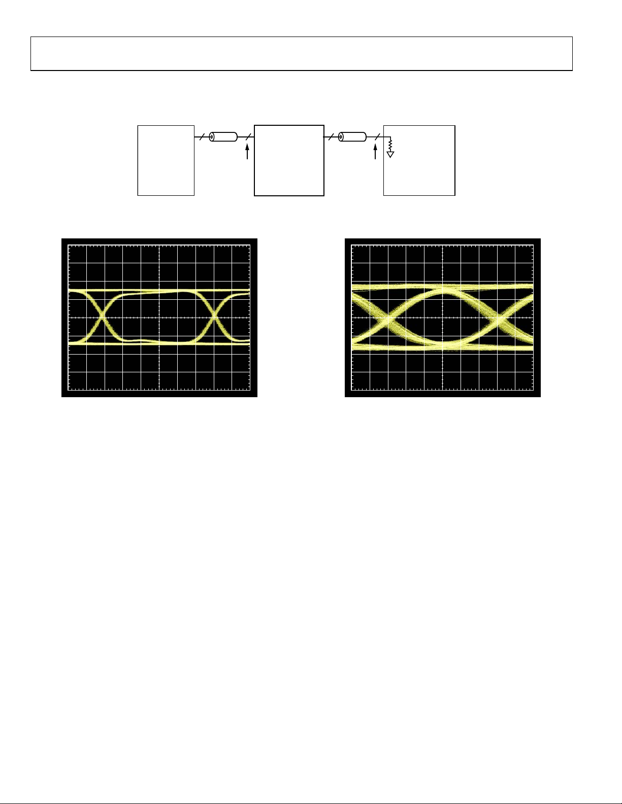
50Ω CABLES
DATA OUT
PATTERN
GENERATOR
2 2
INPUT
PIN
OUTPUT
AD8158
AC-COUPLED
EVALUATION
BOARD
Figure 4. Standard Test Circuit (No Channel)
50Ω CABLES
2 2
PIN
50Ω
TP2TP1
OSCILLOSCOPE
HIGH SPEED
SAMPLING
06646-004
200mV/DI
25ps/DIV
Figure 5. 6.5 Gbps Input Eye (TP1 from Figure 4)
06646-005
200mV/DI
25ps/DIV
Figure 6. 6.5 Gbps Output Eye, No Channel (TP2 from Figure 4)
06646-006
Rev. B | Page 10 of 36
AD8158
V
V
V
V
V
200mV/DI
25ps/DIV
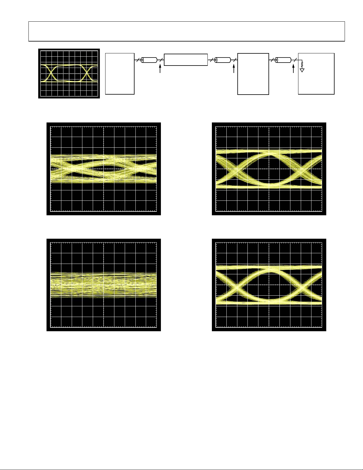
REFERENCE EYE DIAGRAM AT TP1
DATA OUT
PATTERN
GENERATOR
50Ω CABLES
2 2
FR4 TEST BACKP LANE
DIFFERENTIAL
STRIPLI NE TRACES
TP1
8mils WI DE, 8mils S P ACE ,
8mils DIEL ECTRIC HEI GHT
TRACE LENGT H S = 20 INCHES,
40 INCHES
Figure 7. Input Equalization Test Circuit
50Ω CABLES
2 2
TP2
INPUT
OUTPUT
PIN
AD8158
AC-COUPLED
EVALUATION
BOARD
50Ω CABLES
2 2
PIN
50Ω
TP3
SAMPLING
OSCILLOSCOPE
HIGH
SPEED
06646-007
200mV/DI
25ps/DIV
06646-008
Figure 8. 6.5 Gbps Input Eye, 20 Inch FR4 Input Channel (TP2 from Figure 7)
200mV/DI
25ps/DIV
06646-009
Figure 9. 6.5 Gbps Input Eye, 40 Inch FR4 Input Channel (TP2 from Figure 7)
200mV/DI
25ps/DIV
06646-010
Figure 10. 6.5 Gbps Output Eye, 20 Inch FR4 Input Channel (TP3 from Figure 7)
200mV/DI
25ps/DIV
06646-011
Figure 11. 6.5 Gbps Output Eye, 40 Inch FR4 Input Channel (TP3 from Figure 7)
Rev. B | Page 11 of 36
 Loading...