ANALOG DEVICES AD8152 Service Manual
34 ⴛ 34, 3.2 Gbps
OUTPUT
LEVEL
DACs
OUTN
OUTP
VTTO
34 ⴛ 34
DIFFERENTIAL
SWITCH MATRIX
34
34
MATRIX
CONNECTION
LATCHES
CONNECTION
DECODE
OUTPUT
LEVEL
LATCHES
CONTROL
LOGIC
INN
VTTI
INP
D[5:0]
A[6:0]
RE
WE
RESET
CS
UPDATE
VEE
VCC
AD8152
34
34
80ps/DIV
100mV/DIV
www.BDTIC.com/ADI
a
Asynchronous Digital Crosspoint Switch
FEATURES
Low Cost
Low Power
2.0 W @ 2.5 V (Outputs Enabled)
<100 mW @ 2.5 V (Outputs Disabled)
34 ⴛ 34, Fully Differential, Nonblocking Array
3.2 Gbps per Port NRZ Data Rate
Wide Power Supply Range: 2.5 V to 3.3 V
LVTTL or LVCMOS Level Control Inputs:
@ 2.5 V to 3.3 V
Low Jitter: 45 ps
Drives a Backplane Directly
Programmable Output Swing
100 mV to 1.6 V Differential
50 ⍀ On-Chip I/O Termination
User Controlled Voltage at the Load
Minimizes Power Dissipation
Dual Rank Latches
Available in 256-Ball Grid Array
APPLICATIONS
Fiber Optic Network Switching
High Speed Serial Backplane Routing to OC-48 with FEC
Gigabit Ethernet
Digital Video (HDTV)
Data Storage Networks
AD8152
FUNCTIONAL BLOCK DIAGRAM
*
GENERAL DESCRIPTION
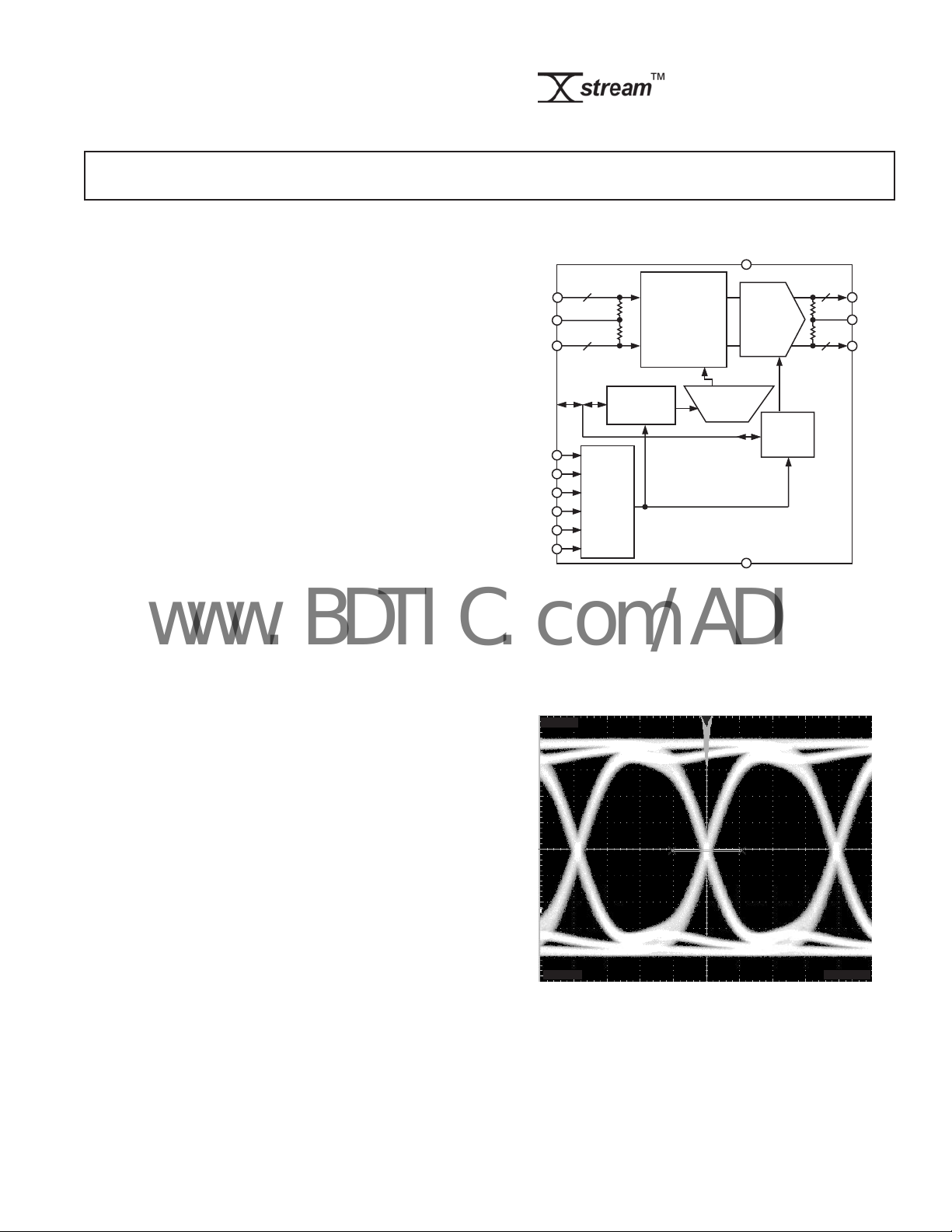
AD8152 is a member of the Xstream line of products and is a
breakthrough in digital switching, offering a large switch array
(34 × 34) on very little power, typically 2.0 W. Additionally, it
operates at data rates up to 3.2 Gbps per port, making it suitable
for Sonet/SDH OC-48 with Forward Error Correction (FEC).
The AD8152’s useful supply voltage range allows the user to
operate at LVPECL/CML data levels down to 2.5 V. The control
interface is LVTTL or LVCMOS compatible on 2.5 V to 3.3 V.
The AD8152’s fully differential signal path reduces jitter and
crosstalk while allowing the use of smaller single-ended voltage
swings. It is offered in a 256-ball SBGA package that operates
over the industrial temperature range of 0°C to 85°C.
Figure 1. Eye Pattern, 3.2 Gbps, PRBS 23
*Patent Pending
REV. A
Information furnished by Analog Devices is believed to be accurate and
reliable. However, no responsibility is assumed by Analog Devices for its
use, nor for any infringements of patents or other rights of third parties that
may result from its use. No license is granted by implication or otherwise
under any patent or patent rights of Analog Devices. Trademarks and
registered trademarks are the property of their respective companies.
One Technology Way, P.O. Box 9106, Norwood, MA 02062-9106, U.S.A.
Tel: 781/329-4700 www.analog.com
Fax: 781/326-8703 © 2003 Analog Devices, Inc. All rights reserved.

AD8152
www.BDTIC.com/ADI
(@ 25ⴗC, VCC = 2.5 V to 3.3 V, VEE = 0 V, RL = 50 ⍀, Differential Output Swing = 800 mV p-p,
ELECTRICAL CHARACTERISTICS
Parameter Condition Min Typ Max Unit
DYNAMIC PERFORMANCE
Max Data Rate/Channel (NRZ) 3.2 Gbps
Channel Jitter Data Rate £ 3.2 Gbps; PRBS 2
RMS Channel Jitter <10 ps
Propagation Delay Input to Output 660 800 ps
Propagation Delay Match ± 50 ± 120 ps
Output Rise/Fall Time 20% to 80% 100 ps
INPUT CHARACTERISTICS
Input Voltage Swing Single-Ended (See TPC 14) 50 1000 mV p-p
Input Voltage Range Common-Mode (See TPC 15) VEE + 0.8 VCC + 0.2 V
Input Bias Current 2 mA
Input Capacitance 2pF
OUTPUT CHARACTERISTICS
Output Voltage Swing Differential (See TPC 18) 100 800 1600 mV p-p
Output Voltage Range VCC – 1.2 VCC + 0.2 V
Output Current 2 32 mA
Output Capacitance 2pF
TERMINATION CHARACTERISTICS
Resistance 43 50 57 W
Temperature Coefficient 0.05 W/∞C
POWER SUPPLY
Operating Range
VCC VEE = 0 V 2.25 3.63 V
Quiescent Current
VCC All Outputs Disabled 32 45 mA
VEE All Outputs Disabled 32 45 mA
LOGIC INPUT CHARACTERISTICS
Input High (VIH) VCC = 3.3 V 2 V
Input Low (VIL) VCC = 3.3 V 0.8 V
Input High (VIH) VCC = 2.5 V 1.7 V
Input Low (VIL) VCC = 2.5 V 0.7 V
LOGIC OUTPUT CHARACTERISTICS
Output High (VOH) VCC = 3.3 V, IOH = –2 mA 2.4 V
Output Low (VOL) VCC = 3.3 V, IOL = +2 mA 0.4 V
Output High (VOH) VCC = 2.5 V, IOH = –100 uA 2.1 V
Output Low (VOL) VCC = 2.5 V, IOL = +100 uA 0.2 V
THERMAL CHARACTERISTICS
Operating Temperature Range 0 85 ∞C
JA
Specifications subject to change without notice.
unless otherwise noted.)
23
– 1 45 ps p-p
All Outputs Enabled 190 mA
All Outputs Enabled 770 mA
to T
T
MIN
Still Air 15 ∞C/W
200 lfpm 12 ∞C/W
400 lfpm 11 ∞C/W
All Outputs Enabled 800 mA
MAX,
REV. A–2–

AD8152
16
0
09010 20 30 40 50 60 70 80
14
8
6
4
2
12
10
AMBIENT TEMPERATURE – ⴗC
MAXIMUM POWER DISSIPATION – W
Tj = 150ⴗC
400 lfpm
200 lfpm
STIL L AIR
www.BDTIC.com/ADI
ABSOLUTE MAXIMUM RATINGS
1
VCC to VEE . . . . . . . . . . . . . . . . . . . . . . . . . . . . . . . . . . 3.7 V
VTTI . . . . . . . . . . . . . . . . . . . . . . . . . . . . . . . . . VCC + 0.6 V
VTTO . . . . . . . . . . . . . . . . . . . . . . . . . . . . . . . . . VCC + 0.6 V
Internal Power Dissipation
2
AD8152 256-Ball SBGA (BP) . . . . . . . . . . . . . . . . . .8.33 W
Input Voltage . . . . . . . . . . . . . . . . . . . . . . . . . . . . VCC + 0.6 V
Differential Input Voltage . . . . . . . . . . . . . . . . . . . . . . . . 1.7 V
Logic Input Voltage . . . . . . VEE – 0.3 V < V
< VCC + 0.6 V
IN
Storage Temperature Range . . . . . . . . . . . . . –65°C to +125°C
Lead Temperature Range . . . . . . . . . . . . . . . . . . . . . . . 300°C
NOTES
1
Stresses above those listed under Absolute Maximum Ratings may cause permanent damage to the device. This is a stress rating only; functional operation of the
device at these or any other conditions above those indicated in the operational
sections of this specification is not implied. Exposure to absolute maximum rating
conditions for extended periods may affect device reliability.
2
Specification is for the device in free air (TA = 25°C): JA = 15°C/W @ still air.
MAXIMUM POWER DISSIPATION
The maximum power that can be safely dissipated by the AD8152 is
limited by the associated rise in junction temperature. The maximum safe junction temperature for plastic encapsulated devices
is determined by the glass transition temperature of the plastic,
approximately 150°C. Temporarily exceeding this limit may cause
Figure 2. Maximum Power Dissipation vs. Temperature
a shift in parametric performance due to a change in the stresses
exerted on the die by the package. Exceeding a junction temperature of 175°C for an extended period can result in device
failure. To ensure proper operation, it is necessary to observe the
maximum power derating curves shown in Figure 2.
ORDERING GUIDE
Model Temperature Range Package Description
AD8152JBP 0°C to 85°C 256-Ball SBGA (27 mm × 27 mm)
AD8152-EVAL Evaluation Board
CAUTION
ESD (electrostatic discharge) sensitive device. Electrostatic charges as high as 4000 V readily
accumulate on the human body and test equipment and can discharge without detection. Although the
AD8152 features proprietary ESD protection circuitry, permanent damage may occur on devices
subjected to high energy electrostatic discharges. Therefore, proper ESD precautions are recommended
to avoid performance degradation or loss of functionality.
REV. A
–3–
AD8152
www.BDTIC.com/ADI
A
BALL GRID ARRAY
20 19 18 17 16 15 14 13 12 11 10 9 8 7 6 5 4 3 2 1
VEE
VEE
VEE
VEE
VEE
O14P
O11P
VCCVCC
O08P
VTTOVTTO
O05P
VTTOVTTO
O02P
VTTO
VCC
VEE
VEE
A
B
C
D
E
F
G
H
J
K
L
M
N
P
R
VEE
VEE
VEEVEE
D1
RESET
CS
RE
VCC
I19N
I19P
VTTI
VTTI
I22P
I22N
VTTI VTTI
I25P
I25N
VCC
VCC
I28P
I28N
VTTI VTTI
I31N
VEE
VEE
D5D4
D2 D3D0
N/C N/C
I17N
I17P
I18PI18N
I20P
I20N
I21N I21P
I23P
I23N
I24P
I24N
I26P I26N
I27N
I27P
I29P I29N
I30PI31P
I30N
VCC
VTTO
O16N
O15P
O16P O15N
VTTO
O14N
O12P
O13P O12N
O11N
O10N
O10P
O09P
O09N
VTTO VTTO
O08N
O07N
O06P O04NO13N
O07P O06N
O05N
O03P O01N
O04P O03N
VTTO
O02N
O00P
O01P O00N
VEE
VCCVCC
A5A6
A4 A3
N/C
N/C
I00N
I00P
I01P I02PI02N
I01N
I03N I03P
I04P
I04N I05N I05P
I06N I06P
I07P
I07N I08N I08P
I09N
I09P
I10P I10N
I12P
I12N
I13NI13P
VEE
VEE
UPDATE
WE
VTTI
VTTI
I11N I11P
VTTI
I14N I14P
VEE
VEE
A1A2
A0
VCC
VTTI
VTTI
VCCVCC
VTTI
B
C
D
E
F
G
H
J
K
L
M
N
P
R
VTTI
VTTI
T
VCC
U
VEE
V
VEE
W
VEE
Y
VCC
VEE
VEE
VEE
I32P I32N
I33N
VEE
VEE
VEE
VEE
VEE
O21P
O29NO30P
VTTO
VTTO
O27P O26N
O27N
O26PO32P
VCC
O28N
VCC
O28P
O32N
O33P
I33P
O33N
VCC VCC
VTTO
O31N
VCC
O31P
O23NO24P
O24N O23P
O25N
VTTOVTTO
O25P
O21NO30N O29P
O22N
O22P
O20N
O20P
VTTO
VTTO
O18N O17P
O19N
O19P
O17NO18P
VTTOVTTO
VTTO
I15N
I16NI16P
VEEVEE
VEE VEE VEE
VCC
I15P
VEE VEE VEE
VEE VEE VEE
20 19 18 17 16 15 14 13 12 11 10 9 8 7 6 5 4 3 2 1
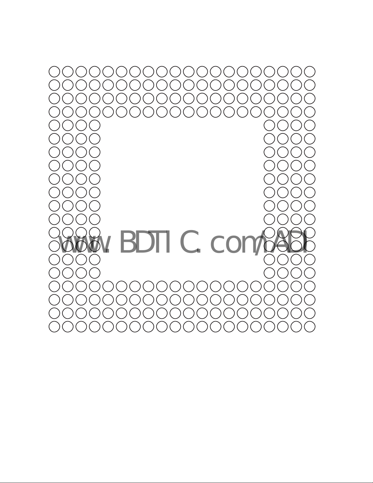
Ball Diagram, View from the Bottom
VTTI
VTTI
VCC VCC
T
U
V
W
Y
REV. A–4–
BALL GRID DESCRIPTIONS
www.BDTIC.com/ADI
AD8152
Ball Mnemonic Type Description
A1 VEE Power Negative Supply
A2 VEE Power Negative Supply
A3 VEE Power Negative Supply
A4 VCC Power Positive Supply
A5 VTTO Power Output Termination Supply
A6 OUT02P I/O High Speed Output
A7 VTTO Power Output Termination Supply
A8 OUT05P I/O High Speed Output
A9 VTTO Power Output Termination Supply
A10 OUT08P I/O High Speed Output
A11 VCC Power Positive Supply
A12 OUT11P I/O High Speed Output
A13 VTTO Power Output Termination Supply
A14 OUT14P I/O High Speed Output
A15 VTTO Power Output Termination Supply
A16 VCC Power Positive Supply
A17 VEE Power Negative Supply
A18 VEE Power Negative Supply
A19 VEE Power Negative Supply
A20 VEE Power Negative Supply
B1 VEE Power Negative Supply
B2 VEE Power Negative Supply
B3 VEE Power Negative Supply
B4 VCC Power Positive Supply
B5 VTTO Power Output Termination Supply
B6 OUT02N I/O High Speed Output Complement
B7 VTTO Power Output Termination Supply
B8 OUT05N I/O High Speed Output Complement
B9 VTTO Power Output Termination Supply
B10 OUT08N I/O High Speed Output Complement
B11 VCC Power Positive Supply
B12 OUT11N I/O High Speed Output Complement
B13 VTTO Power Output Termination Supply
B14 OUT14N I/O High Speed Output Complement
B15 VTTO Power Output Termination Supply
B16 VCC Power Positive Supply
B17 VEE Power Negative Supply
B18 VEE Power Negative Supply
B19 VEE Power Negative Supply
B20 VEE Power Negative Supply
C1 VEE Power Negative Supply
C2 VEE Power Negative Supply
C3 A5 Control Output Address Pin (MSB)
C4 A6 Control Output Address Pin (Bank Des.)
C5 OUT00P I/O High Speed Output
C6 OUT01N I/O High Speed Output Complement
C7 OUT03P I/O High Speed Output
C8 OUT04N I/O High Speed Output Complement
C9 OUT06P I/O High Speed Output
C10 OUT07N I/O High Speed Output Complement
C11 OUT09P I/O High Speed Output
Ball Mnemonic Type Description
C12 OUT10N I/O High Speed Output Complement
C13 OUT12P I/O High Speed Output
C14 OUT13N I/O High Speed Output Complement
C15 OUT15P I/O High Speed Output
C16 OUT16N I/O High Speed Output Complement
C17 D5 Control Input Address Pin (MSB)
C18 D4 Control Input Address Pin
C19 VEE Power Negative Supply
C20 VEE Power Negative Supply
D1 A1 Control Output Address Pin
D2 A2 Control Output Address Pin
D3 A3 Control Output Address Pin
D4 A4 Control Output Address Pin
D5 OUT00N I/O High Speed Output Complement
D6 OUT01P I/O High Speed Output
D7 OUT03N I/O High Speed Output Complement
D8 OUT04P I/O High Speed Output
D9 OUT06N I/O High Speed Output Complement
D10 OUT07P I/O High Speed Output
D11 OUT09N I/O High Speed Output Complement
D12 OUT10P I/O High Speed Output
D13 OUT12N I/O High Speed Output Complement
D14 OUT13P I/O High Speed Output
D15 OUT15N I/O High Speed Output Complement
D16 OUT16P I/O High Speed Output
D17 D3 Control Input Address Pin
D18 D2 Control Input Address Pin
D19 D1 Control Input Address Pin
D20 D0 Control Input Address Pin (LSB)
E1 A0 Control Output Address Pin (LSB)
E2 UPDATE Control Second Rank Write Enable
E3 N/C Reserved Do Not Connect
E4 N/C Reserved Do Not Connect
E17 N/C Reserved Do Not Connect
E18 N/C Reserved Do Not Connect
E19 RESET Control Reset/Disable Outputs
E20 CS Control Chip Select Enable
F1 VCC Power Positive Supply
F2 WE Control First Rank Write Enable
F3 IN00P I/O High Speed Input
F4 IN00N I/O High Speed Input Complement
F17 IN17N I/O High Speed Input Complement
F18 IN17P I/O High Speed Input
F19 RE Control Readback Enable
F20 VCC Power Positive Supply
G1 IN02P I/O High Speed Input
G2 IN02N I/O High Speed Input Complement
G3 IN01N I/O High Speed Input Complement
G4 IN01P I/O High Speed Input
G17 IN18P I/O High Speed Input
G18 IN18N I/O High Speed Input Complement
REV. A
–5–

AD8152
www.BDTIC.com/ADI
BALL GRID DESCRIPTIONS (continued)
Ball Mnemonic Type Description
G19 IN19N I/O High Speed Input Complement
G20 IN19P I/O High Speed Input
H1 VTTI Power Input Termination Supply
H2 VTTI Power Input Termination Supply
H3 IN03P I/O High Speed Input
H4 IN03N I/O High Speed Input Complement
H17 IN20N I/O High Speed Input Complement
H18 IN20P I/O High Speed Input
H19 VTTI Power Input Termination Supply
H20 VTTI Power Input Termination Supply
J1 IN05P I/O High Speed Input
J2 IN05N I/O High Speed Input Complement
J3 IN04N I/O High Speed Input Complement
J4 IN04P I/O High Speed Input
J17 IN21P I/O High Speed Input
J18 IN21N I/O High Speed Input Complement
J19 IN22N I/O High Speed Input Complement
J20 IN22P I/O High Speed Input
K1 VTTI Power Input Termination Supply
K2 VTTI Power Input Termination Supply
K3 IN06P I/O High Speed Input Complement
K4 IN06N I/O High Speed Input
K17 IN23N I/O High Speed Input Complement
K18 IN23P I/O High Speed Input
K19 VTTI Power Input Termination Supply
K20 VTTI Power Input Termination Supply
L1 IN08P I/O High Speed Input
L2 IN08N I/O High Speed Input Complement
L3 IN07N I/O High Speed Input Complement
L4 IN07P I/O High Speed Input
L17 IN24P I/O High Speed Input
L18 IN24N I/O High Speed Input Complement
L19 IN25N I/O High Speed Input Complement
L20 IN25P I/O High Speed Input
M1 VCC Power Positive Supply
M2 VCC Power Positive Supply
M3 IN09P I/O High Speed Input
M4 IN09N I/O High Speed Input Complement
M17 IN26N I/O High Speed Input Complement
M18 IN26P I/O High Speed Input
M19 VCC Power Positive Supply
M20 VCC Power Positive Supply
N1 IN11P I/O High Speed Input
N2 IN11N I/O High Speed Input Complement
N3 IN10N I/O High Speed Input Complement
N4 IN10P I/O High Speed Input
N17 IN27P I/O High Speed Input
N18 IN27N I/O High Speed Input Complement
N19 IN28N I/O High Speed Input Complement
N20 IN28P I/O High Speed Input
P1 VTTI Power Input Termination Supply
Ball Mnemonic Type Description
P2 VTTI Power Input Termination Supply
P3 IN12P I/O High Speed Input
P4 IN12N I/O High Speed Input Complement
P17 IN29N I/O High Speed Input Complement
P18 IN29P I/O High Speed Input
P19 VTTI Power Input Termination Supply
P20 VTTI Power Input Termination Supply
R1 IN14P I/O High Speed Input
R2 IN14N I/O High Speed Input Complement
R3 IN13N I/O High Speed Input Complement
R4 IN13P I/O High Speed Input
R17 IN30P I/O High Speed Input
R18 IN30N I/O High Speed Input Complement
R19 IN31N I/O High Speed Input Complement
R20 IN31P I/O High Speed Input
T1 VTTI Power Input Termination Supply
T2 VTTI Power Input Termination Supply
T3 IN15P I/O High Speed Input
T4 IN15N I/O High Speed Input Complement
T17 IN32N I/O High Speed Input Complement
T18 IN32P I/O High Speed Input
T19 VTTI Power Input Termination Supply
T20 VTTI Power Input Termination Supply
U1 VCC Power Positive Supply
U2 VCC Power Positive Supply
U3 IN16N I/O High Speed Input Complement
U4 IN16P I/O High Speed Input
U5 OUT17N I/O High Speed Output Complement
U6 OUT18P I/O High Speed Output
U7 OUT20N I/O High Speed Output Complement
U8 OUT21P I/O High Speed Output
U9 OUT23N I/O High Speed Output Complement
U10 OUT24P I/O High Speed Output
U11 OUT26N I/O High Speed Output Complement
U12 OUT27P I/O High Speed Output
U13 OUT29N I/O High Speed Output
U14 OUT30P I/O High Speed Output
U15 OUT32N I/O High Speed Output Complement
U16 OUT33P I/O High Speed Output
U17 IN33P I/O High Speed Input
U18 IN33N I/O High Speed Input Complement
U19 VCC Power Positive Supply
U20 VCC Power Positive Supply
V1 VEE Power Negative Supply
V2 VEE Power Negative Supply
V3 VEE Power Negative Supply
V4 VEE Power Negative Supply
V5 OUT17P I/O High Speed Output
V6 OUT18N I/O High Speed Output Complement
V7 OUT20P I/O High Speed Output
V8 OUT21N I/O High Speed Output Complement
REV. A–6–
BALL GRID DESCRIPTIONS (continued)
www.BDTIC.com/ADI
AD8152
Ball Mnemonic Type Description
V9 OUT23P I/O High Speed Output
V10 OUT24N I/O High Speed Output Complement
V11 OUT26P I/O High Speed Output
V12 OUT27N I/O High Speed Output Complement
V13 OUT29P I/O High Speed Output
V14 OUT30N I/O High Speed Output Complement
V15 OUT32P I/O High Speed Output
V16 OUT33N I/O High Speed Output Complement
V17 VEE Power Negative Supply
V18 VEE Power Negative Supply
V19 VEE Power Negative Supply
V20 VEE Power Negative Supply
W1 VEE Power Negative Supply
W2 VEE Power Negative Supply
W3 VEE Power Negative Supply
W4 VCC Power Positive Supply
W5 VTTO Power Output Termination Supply
W6 OUT19N I/O High Speed Output Complement
W7 VTTO Power Output Termination Supply
W8 OUT22N I/O High Speed Output Complement
W9 VTTO Power Output Termination Supply
W10 OUT25N I/O High Speed Output Complement
W11 VCC Power Positive Supply
W12 OUT28N I/O High Speed Output Complement
W13 VTTO Power Output Termination Supply
W14 OUT31N I/O High Speed Output Complement
Ball Mnemonic Type Description
W15 VTTO Power Output Termination Supply
W16 VCC Power Positive Supply
W17 VEE Power Negative Supply
W18 VEE Power Negative Supply
W19 VEE Power Negative Supply
W20 VEE Power Negative Supply
Y1 VEE Power Negative Supply
Y2 VEE Power Negative Supply
Y3 VEE Power Negative Supply
Y4 VCC Power Positive Supply
Y5 VTTO Power Output Termination Supply
Y6 OUT19P I/O High Speed Output
Y7 VTTO Power Output Termination Supply
Y8 OUT22P I/O High Speed Output
Y9 VTTO Power Output Termination Supply
Y10 OUT25P I/O High Speed Output
Y11 VCC Power Positive Supply
Y12 OUT28P I/O High Speed Output
Y13 VTTO Power Output Termination Supply
Y14 OUT31P I/O High Speed Output
Y15 VTTO Power Output Termination Supply
Y16 VCC Power Positive Supply
Y17 VEE Power Negative Supply
Y18 VEE Power Negative Supply
Y19 VEE Power Negative Supply
Y20 VEE Power Negative Supply
REV. A
–7–
AD8152–Typical Performance Characteristics
www.BDTIC.com/ADI
(2.5 V Supply, VCC = VTTI = VTTO, Data Rate = 3.2 Gbps;
PRBS 223–1; Differential Output Swing = 800 mV p-p; RL = 50 ⍀; Input Amplitude = 0.4 V p-p Single-Ended; unless otherwise noted.)
100mV/DIV
100mV/DIV
80ps/DIV
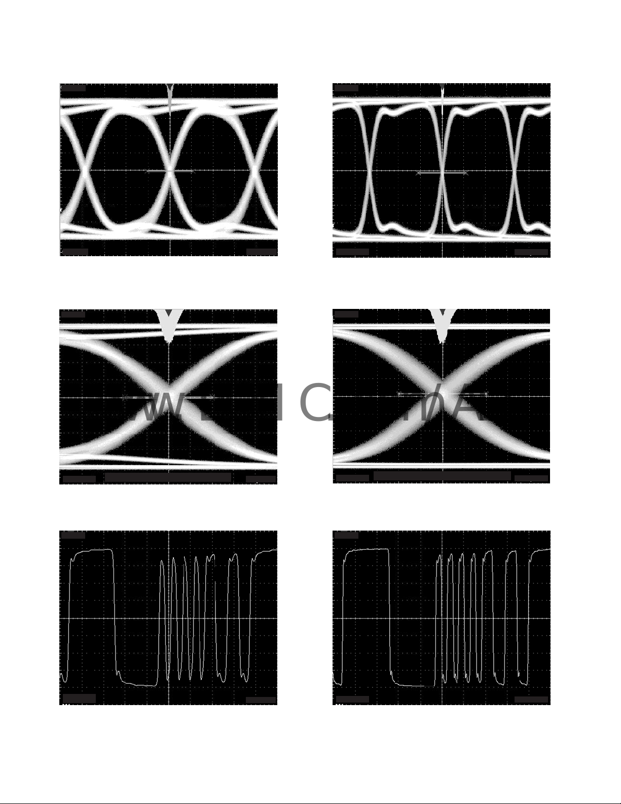
TPC 1. Eye Pattern 3.2 Gbps
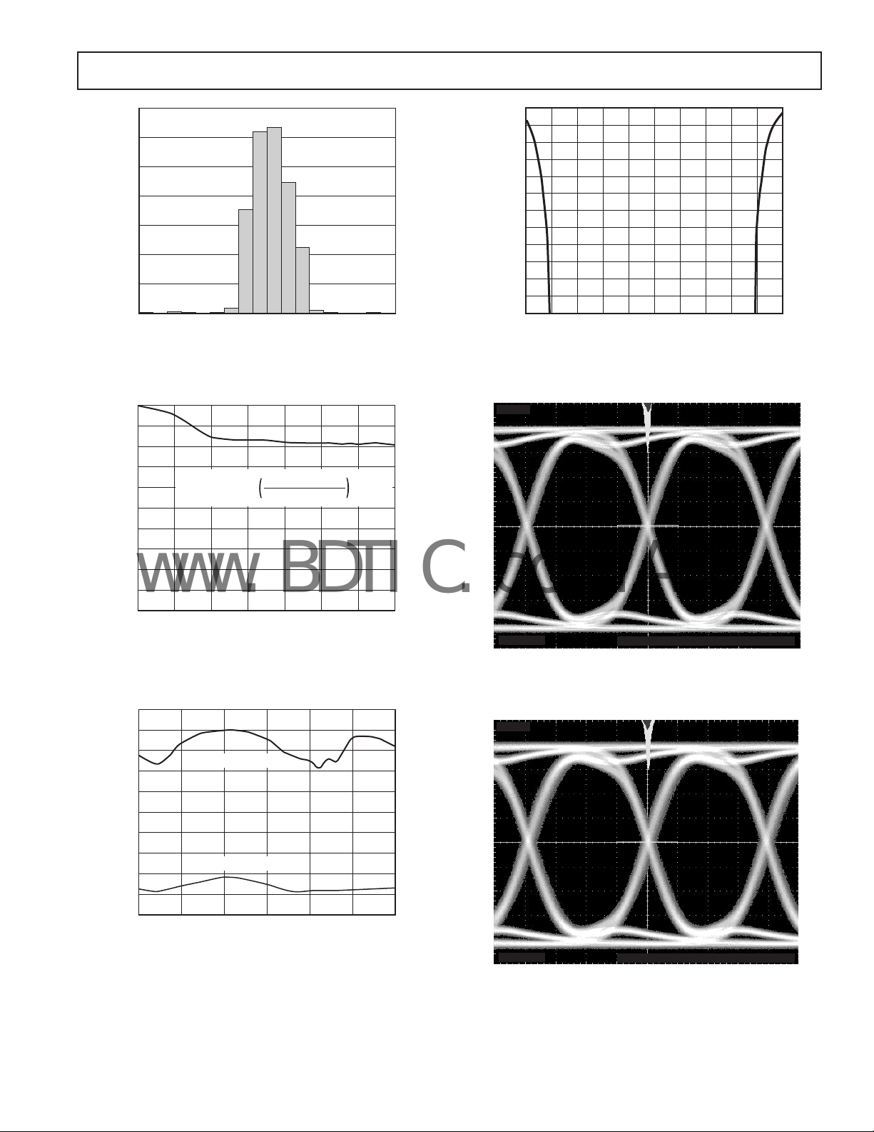
PEAK-PEAK JITTER = 35ps STD DEV = 5.1ps
20ps/DIV
TPC 2. Jitter @ 3.2 Gbps
100mV/DIV
200ps/DIV
TPC 4. Eye Pattern 1.5 Gbps
100mV/DIV
PEAK-PEAK JITTER = 35ps STD DEV = 5.2ps
20ps/DIV
TPC 5. Jitter @ 1.5 Gbps
100mV/DIV
1.2ns/DIV
TPC 3. Response, 3.2 Gbps, 32-Bit Pattern
1111 1111 0000 0000 1010 1010 1100 1100
100mV/DIV
TPC 6. Response, 1.5 Gbps, 32-Bit Pattern
1111 1111 0000 0000 1010 1010 1100 1100
2.5ns/DIV
REV. A–8–
AD8152
UNIT INTERVAL
1.E+00
0.1
–0.5
BIT ERROR RATE
–0.4
–0.3 –0.2 –0.1 0 0.2 0.3 0.4 0.5
1.E–01
1.E–02
1.E–03
1.E–04
1.E–05
1.E–06
1.E–07
1.E–08
1.E–09
1.E–10
1.E–11
1.E–12
100mV/DIV
80ps/DIV
PEAK-PEAK JITTER = 35ps STD DEV = 5.6ps
100mV/DIV
80ps/DIV
PEAK-PEAK JITTER = 46ps STD DEV = 6.5ps
www.BDTIC.com/ADI
1400
1200
1000
800
600
FREQUENCY
400
200
0
–40 –20–30 –10 10
–50 30
DUTY CYCLE DISTORTION – ps
020
BIN WIDTH = 5ps
TPC 7. Duty Cycle Distortion Distribution
100
90
80
70
60
50
40
EYE HEIGHT – %
30
20
10
0
1.0
0.5
%EYE HEIGHT =
1.5
V
@ DATA RATE
OUT
V
@ 0.5Gbps
OUT
2.0 2.5 3.0 3.5
DATA RATE – Gbps
40 50
TPC 10. Bit Error Rate vs. Unit Interval
ⴛ100
4.0
TPC 8. Eye Height vs. Data Rate
TPC 11. Crosstalk, 3.2 Gbps, Attack Signal OFF
(See TPC 25)
50
45
40
35
30
25
20
JITTER – ps
15
10
REV. A
5
0
1.0
PEAK-PEAK JITTER
STANDARD DEVIATION
2.0 2.5 3.0 3.5
1.5
DATA RATE – Gbps
TPC 9. Jitter vs. Data Rate
4.0
TPC 12. Crosstalk, 3.2 Gbps, Attack Signal ON
(See TPC 25)
–9–
AD8152
www.BDTIC.com/ADI
55
50
45
40
35
PEAK-PEAK JITTER – ps
30
25
1.5 Gbps
10 20 30 40
0
3.2 Gbps
50
TEMPERATURE – ⴗC
60 70 80 90
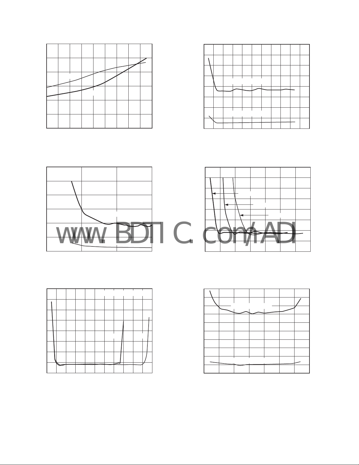
TPC 13. Single Point Jitter vs. Temperature
120
100
80
60
JITTER – ps
40
20
0
0
PEAK–PEAK JITTER
STANDARD DEVIATION
10 100 1000
INPUT AMPLITUDE – mV
80
70
60
50
40
JITTER – ps
30
20
10
0
PEAK-PEAK JITTER
STANDARD DEVIATION
TPC 16. Jitter vs. Supply
160
140
120
100
80
60
PEAK-PEAK JITTER – ps
40
20
0
–1.4
–1.2 –1.0 –0.6 –0.4 –0.2 0
SUPPLY VOLTAGE – V
I
= 16mA
OUT
I
= 24mA
OUT
I
OUT
–0.8
VOL – V
4.03.63.43.23.02.82.62.42.22.01.8 3.8
= 32mA
TPC 14. Jitter vs. Single-Ended Input Amplitude
180
160
140
120
100
80
PEAK-PEAK JITTER – ps
60
40
20
INPUT AMPLITUDE = 50mV p-p
@2.5V
INPUT CML – V
@3.3V
3.83.22.92.62.32.01.71.41.10.80.5 3.5
TPC 15. Jitter vs. Input Common-Mode Level
TPC 17. Jitter vs. V
50
45
40
35
30
25
20
JITTER – ps
15
10
5
0
0
STANDARD DEVIATION
5101520253035
PEAK–PEAK JITTER
(Relative to VCC)
OL
I
– mA
OUT
TPC 18. Jitter vs. Programmed I
OUT
REV. A–10–
 Loading...