ANALOG DEVICES AD8150 Service Manual
33 × 17, 1.5 Gbps Digital
–
www.BDTIC.com/ADI
FEATURES
Low cost
33 × 17, fully differential, nonblocking array
>1.5 Gbps per port NRZ data rate
Wide power supply range: +5 V, +3.3 V, −3.3 V, −5 V
Low power
400 mA (outputs enabled)
30 mA (outputs disabled)
PECL and ECL compatible
CMOS/TTL-level control inputs: 3 V to 5 V
Low jitter: <50 ps p-p
No heat sinks required
Drives a backplane directly
Programmable output current
Optimize termination impedance
User-controlled voltage at the load
Minimize power dissipation
Individual output disable for busing and building
Larger arrays
Double row latch
Buffered inputs
Available in 184-lead LQFP
APPLICATIONS
HD and SD digital video
Fiber optic network switching
GENERAL DESCRIPTION
AD81501 is a member of the Xstream line of products and is a
breakthrough in digital switching, offering a large switch array
(33 × 17) on very little power, typically less than 1.5 W.
Additionally, it operates at data rates in excess of 1.5 Gbps per
port, making it suitable for HDTV applications. Further, the
pricing of the AD8150 makes it affordable enough to be used
for SD applications. The AD8150 is also useful for OC-24
optical network switching.
The AD8150’s flexible supply voltages allow the user to operate
with either PECL or ECL data levels and will operate down to
3.3 V for further power reduction. The control interface is
CMOS/TTL compatible (3 V to 5 V).
Its fully differential signal path reduces jitter and crosstalk while
allowing the use of smaller single-ended voltage swings. The
AD8150 is offered in a 184-lead LQFP package that operates
over the industrial temperature range of 0°C to 85°C.
UPDATE
RESET
1
Patent pending.
CS
RE
D
A
WE
500mV
100mV/
500mV
Crosspoint Switch
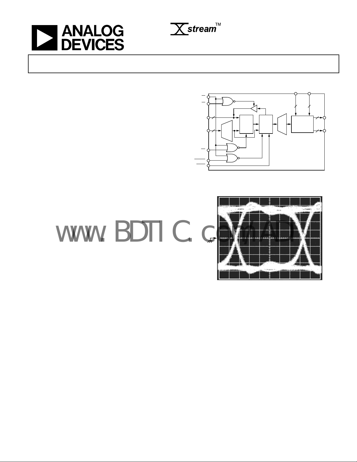
FUNCTIONAL BLOCK DIAGRAM
7
5
DIV
FIRST
RANK
LATCH
OUTPUT
ADDRESS
DECODER
Figure 1. Functional Block Diagram
Figure 2. Output Eye Pattern, 1.5 Gbps
17
7-BIT
SECOND
RANK
×
×
17
7-BIT
LATCH
100ps/DIV
INPUT
DECODERS
AD8150
INP INN
33 33
17
33 × 17
DIFFERENTIAL
SWITCH
MATRIX
17
AD8150
OUTP
OUTN
01074-001
01074-002
Rev. A
Information furnished by Analog Devices is believed to be accurate and reliable.
However, no responsibility is assumed by Analog Devices for its use, nor for any
infringements of patents or other rights of third parties that may result from its use.
Specifications subject to change without notice. No license is granted by implication
or otherwise under any patent or patent rights of Analog Devices. Trademarks and
registered trademarks are the property of their respective owners.
One Technology Way, P.O. Box 9106, Norwood, MA 02062-9106, U.S.A.
Tel: 781.329.4700 www.analog.com
Fax: 781.461.3113 © 2005 Analog Devices, Inc. All rights reserved.

AD8150
www.BDTIC.com/ADI
TABLE OF CONTENTS
Specifications..................................................................................... 3
High Speed Data Outputs (OUTyyP, OUTyyN) .................... 23
Absolute Maximum Ratings............................................................ 4
Maximum Power Dissipiation.................................................... 4
ESD Caution.................................................................................. 4
Pin Configuration and Function Descriptions............................. 5
Typical Performance Characteristics ............................................. 9
Test Circuit ......................................................................................13
Control Interface............................................................................. 14
Control Interface Truth Tables ................................................. 14
Control Interface Timing Diagrams ........................................15
Control Interface Programming Example .............................. 20
Control Interface Description................................................... 21
Control Pin Description............................................................ 21
Control Interface Translators.................................................... 22
Circuit Description......................................................................... 23
High Speed Data Inputs (INxxP, INxxN)................................ 23
Output Current Set Pin (REF).................................................. 24
Power Supplies............................................................................ 25
Power Dissipation....................................................................... 27
Heat Sinking................................................................................ 28
Applications..................................................................................... 29
AD8150 Input and Output Busing........................................... 29
Evaluation Board............................................................................ 30
Configuration Programming.................................................... 30
Power Supplies............................................................................ 30
Software Installation.................................................................. 30
Software Operation.................................................................... 31
PCB Layout...................................................................................... 32
Outline Dimensions....................................................................... 42
Ordering Guide .......................................................................... 42
REVISION HISTORY
9/05—Rev. 0 t o R e v. A
Updated Format..................................................................Universal
Change to Absolute Maximum Ratings......................................... 4
Changes to Maximum Power Dissipation Section....................... 4
Change to Figure 3 ........................................................................... 4
Changes to Figure 40...................................................................... 26
Updated Outline Dimensions....................................................... 42
Changes to Ordering Guide.......................................................... 42
Revision 0: Initial Version
Rev. A | Page 2 of 44

AD8150
www.BDTIC.com/ADI
SPECIFICATIONS
At 25°C, VCC = 3.3 V to 5 V, VEE = 0 V, RL = 50 Ω (see Figure 25), I
Table 1
Parameter Conditions Min Typ Max Unit
DYNAMIC PERFORMANCE
Max Data Rate/Channel (NRZ) 1.5 Gbps
Channel Jitter Data rate < 1.5 Gbps 50 ps p-p
RMS Channel Jitter VCC = 5 V 10 ps
Propagation Delay Input to output 650 ps
Propagation Delay Match 50 100 ps
Output Rise/Fall Time 20% to 80% 100 ps
INPUT CHARACTERISTICS
Input Voltage Swing Differential 200 1000 mV p-p
Input Voltage Range Common mode VCC − 2 VCC V
Input Bias Current 2 μA
Input Capacitance 2 pF
Input VIN High VCC − 1.2 VCC − 0.2 V
Input VIN Low VCC − 2.4 VCC − 1.4 V
OUTPUT CHARACTERISTICS
Output Voltage Swing Differential (see Figure 25) 800 mV p-p
Output Voltage Range VCC − 1.8 VCC V
Output Current 5 25 mA
Output Capacitance 2 pF
POWER SUPPLY
Operating Range
PECL, VCC V
ECL, VEE V
VDD 3 5 V
VSS 0 V
Quiescent Current
VDD 2 mA
VEE All outputs enabled, I
T
All outputs disabled 30 mA
THERMAL CHARACTERISTICS
Operating Temperature Range 0 85 °C
θJA 30 °C/W
LOGIC INPUT CHARACTERISTICS VDD = 3 V dc to 5 V dc
Input VIN High 1.9 VDD V
Input VIN Low 0 0.9 V
= 0 V 3.3 5 V
EE
= 0 V −5 −3.3 V
CC
to T
MIN
450 mA
MAX
= 16 mA, unless otherwise noted.
OUT
= 16 mA 400 mA
OUT
Rev. A | Page 3 of 44
AD8150
www.BDTIC.com/ADI
ABSOLUTE MAXIMUM RATINGS
Table 2.
Parameter Rating
Supply Voltage VDD − VEE 10.5 V
Internal Power Dissipation1
AD8150 184-Lead Plastic LQFP (ST) 4.2 W
Differential Input Voltage VCC − VEE
Output Short-Circuit Duration
Storage Temperature Range2 −65°C to +125°C
1
Specification is for device in free air (TA = 25°C):
184-lead plastic LQFP (ST): θJA = 30°C/W.
2
Maximum reflow temperatures are to JEDEC industry standard J-STD-020.
Observe power
derating curves
MAXIMUM POWER DISSIPIATION
The maximum power that can be safely dissipated by the
AD8150 is limited by the associated rise in junction
temperature. The maximum safe junction temperature for
plastic encapsulated devices is determined by the glass
transition temperature of the plastic, approximately 125°C.
Temporarily exceeding this limit may cause a shift in
parametric performance due to a change in the stresses exerted
on the die by the package. Exceeding a junction temperature of
125°C for an extended period can result in device failure.
While the AD8150 is internally short-circuit protected, this may
not be sufficient to guarantee that the maximum junction
temperature (125°C) is not exceeded under all conditions. To
ensure proper operation, it is necessary to observe the
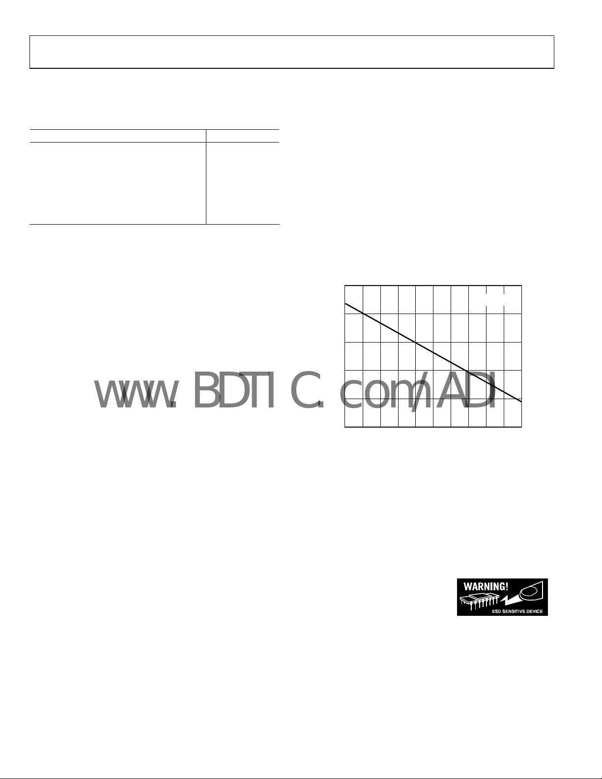
maximum power derating curves shown in
Figure 3.
Stresses above those listed under Absolute Maximum Ratings
may cause permanent damage to the device. This is a stress
rating only; functional operation of the device at these or any
other conditions above those indicated in the operational
section of this specification is not implied. Exposure to absolute
maximum rating conditions for extended periods may affect
device reliability.
6
5
4
3
2
MAXIMUM POWER DISSIPATION (W)
1
–10 9080706050403020100
Figure 3. Maximum Power Dissipation vs. Temperature
AMBIENT TEMPERATURE (°C)
TJ = 150°C
01074-003
ESD CAUTION
ESD (electrostatic discharge) sensitive device. Electrostatic charges as high as 4000 V readily accumulate on
the human body and test equipment and can discharge without detection. Although this product features
proprietary ESD protection circuitry, permanent damage may occur on devices subjected to high energy
electrostatic discharges. Therefore, proper ESD precautions are recommended to avoid performance
degradation or loss of functionality.
Rev. A | Page 4 of 44
AD8150
www.BDTIC.com/ADI
PIN CONFIGURATION AND FUNCTION DESCRIPTIONS
V
IN20P
IN20N
V
IN21P
IN21N
V
IN22P
IN22N
V
IN23P
IN23N
V
IN24P
IN24N
V
IN25P
IN25N
V
IN26P
IN26N
V
IN27P
IN27N
V
IN28P
IN28N
V
IN29P
IN29N
V
IN30P
IN30N
V
IN31P
IN31N
V
IN32P
IN32N
V
V
V
OUT16N
OUT16P
VEEA16
V
EE
CCVDD
IN19N
IN19P
IN18N
IN18P
IN17N
179
OUT14P
178
A14
V
IN17P
177
176
175
A13
EE
EE
V
OUT13P
OUT13N
VEEVEEVEEVEEV
184
183
182
181
180
1
EE
EE
EE
EE
EE
EE
EE
EE
EE
EE
EE
EE
EE
EE
CC
EE
EE
PIN 1
2
INDICATOR
3
4
5
6
7
8
9
10
11
12
13
14
15
16
17
18
19
20
21
22
23
24
25
26
27
28
29
30
31
32
33
34
35
36
37
38
39
40
41
42
43
44
45
46
4748495051525354555657
EE
V
A15
EE
V
OUT15P
OUT15N
OUT14N
V
IN16N
174
58
OUT12N
IN16P
173
OUT12P
RESETCSREWEUPDATEA0A1A2A3A4D0D1D2D3D4D5D6
171
170
169
172
596061626364656667
A12
A11
EE
EE
V
V
OUT11P
OUT11N
168
OUT10N
167
OUT10P
166
A10
V
EE
165
164
163
162
161
160
159
157
156
155
158
AD8150
184L LQFP
TOP VIEW
(Not to Scale)
68
6970717274757677787379808182848586
A9
A8
EE
EE
V
V
OUT09P
OUT08P
OUT09N
OUT08N
OUT07N
OUT07P
154
A7
A6
EE
EE
V
V
OUT06P
OUT06N
REF
EE
REF
VSSVCCVEEVEEVEEV
153
152
151
A5
EE
V
OUT05P
OUT05N
V
150
OUT04N
149
OUT04P
IN15N
IN15P
IN14N
IN14P
147
146
145
144
143
148
A4
EE
V
OUT03P
OUT03N
142
87838889909192
A3
A2
EE
EE
V
V
OUT02P
OUT02N
IN13N
141
OUT01N
IN13P
140
OUT01P
EE
139
138
V
EE
137
IN12N
136
IN12P
135
V
EE
134
IN11N
133
IN11P
132
V
EE
131
IN10N
130
IN10P
129
V
EE
128
IN09N
127
IN09P
126
V
EE
125
IN08N
124
IN08P
123
V
EE
122
IN07N
121
IN07P
120
V
EE
119
IN06N
118
IN06P
117
V
EE
116
IN05N
115
IN05P
114
V
EE
113
IN04N
112
IN04P
111
V
EE
110
IN03N
109
IN03P
108
V
EE
107
IN02N
106
IN02P
105
V
EE
104
IN01N
103
IN01P
102
V
EE
101
IN00N
100
IN00P
99
V
EE
98
V
CC
97
VEEA0
96
OUT00P
95
OUT00N
94
V
EE
93
V
EE
A1
EE
V
01074-004
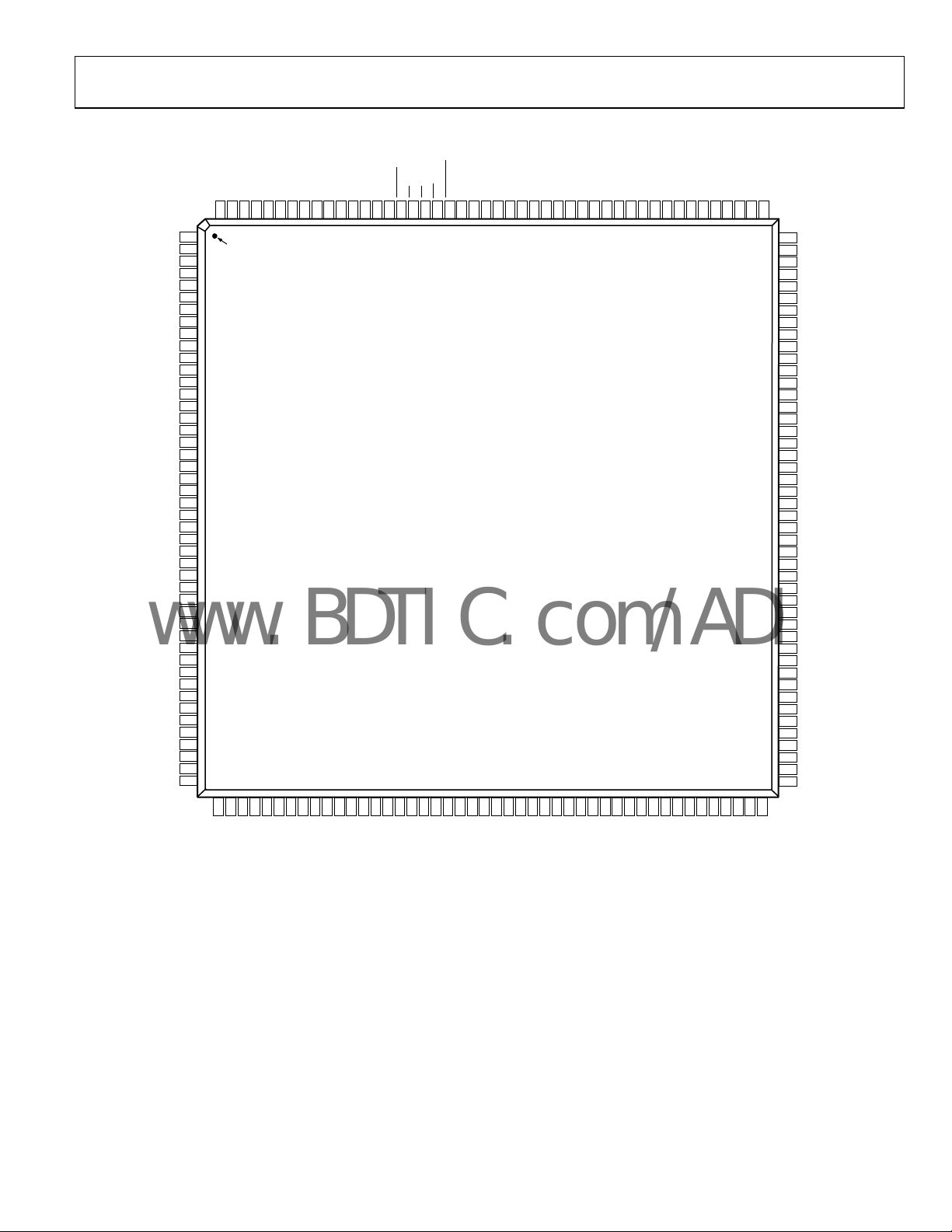
Figure 4. Pin Configuration
Rev. A | Page 5 of 44

AD8150
www.BDTIC.com/ADI
Table 3. Pin Function Descriptions
Pin No. Mnemonic Type Description
V
1, 4, 7, 10, 13, 16, 19, 22, 25, 28, 31,
34, 37, 40, 42, 46, 47, 92, 93, 99, 102,
105, 108, 111, 114, 117, 120, 123,
126, 129, 132, 135, 138, 139, 142,
145, 148, 172, 175, 178, 181, 184
2 IN20P PECL High Speed Input
3 IN20N PECL High Speed Input Complement
5 IN21P PECL High Speed Input
6 IN21N PECL High Speed Input Complement
8 IN22P PECL High Speed Input
9 IN22N PECL High Speed Input Complement
11 IN23P PECL High Speed Input
12 IN23N PECL High Speed Input Complement
14 IN24P PECL High Speed Input
15 IN24N PECL High Speed Input Complement
17 IN25P PECL High Speed Input
18 IN25N PECL High Speed Input Complement
20 IN26P PECL High Speed Input
21 IN26N PECL High Speed Input Complement
23 IN27P PECL High Speed Input
24 IN27N PECL High Speed Input Complement
26 IN28P PECL High Speed Input
27 IN28N PECL High Speed Input Complement
29 IN29P PECL High Speed Input
30 IN29N PECL High Speed Input Complement
32 IN30P PECL High Speed Input
33 IN30N PECL High Speed Input Complement
35 IN31P PECL High Speed Input
36 IN31N PECL High Speed Input Complement
38 IN32P PECL High Speed Input
39 IN32N PECL High Speed Input Complement
41, 98, 149, 171 VCC Power supply Most Positive PECL Supply (common with other points labeled VCC)
43 OUT16N PECL High Speed Output Complement
44 OUT16P PECL High Speed Output
45 VEEA16 Power supply Most Negative PECL Supply (unique to this output)
48 OUT15N PECL High Speed Output Complement
49 OUT15P PECL High Speed Output
50 VEEA15 Power supply Most Negative PECL Supply (unique to this output)
51 OUT14N PECL High Speed Output Complement
52 OUT14P PECL High Speed Output
53 VEEA14 Power supply Most Negative PECL Supply (unique to this output)
54 OUT13N PECL High Speed Output Complement
55 OUT13P PECL High Speed Output
56 VEEA13 Power supply Most Negative PECL Supply (unique to this output)
57 OUT12N PECL High Speed Output Complement
58 OUT12P PECL High Speed Output
59 VEEA12 Power supply Most Negative PECL Supply (unique to this output)
60 OUT11N PECL High Speed Output Complement
61 OUT11P PECL High Speed Output
62 VEEA11 Power supply Most Negative PECL Supply (unique to this output)
63 OUT10N PECL High Speed Output Complement
64 OUT10P PECL High Speed Output
Power supply Most Negative PECL Supply (common with other points labeled VEE)
EE
Rev. A | Page 6 of 44

AD8150
www.BDTIC.com/ADI
Pin No. Mnemonic Type Description
65 VEEA10 Power supply Most Negative PECL Supply (unique to this output)
66 OUT09N PECL High Speed Output Complement
67 OUT09P PECL High Speed Output
68 VEEA9 Power supply Most Negative PECL Supply (unique to this output)
69 OUT08N PECL High Speed Output Complement
70 OUT08P PECL High Speed Output
71 VEEA8 Power supply Most Negative PECL Supply (unique to this output)
72 OUT07N PECL High Speed Output Complement
73 OUT07P PECL High Speed Output
74 VEEA7 Power supply Most Negative PECL Supply (unique to this output)
75 OUT06N PECL High Speed Output Complement
76 OUT06P PECL High Speed Output
77 VEEA6 Power supply Most Negative PECL Supply (unique to this output)
78 OUT05N PECL High Speed Output Complement
79 OUT05P PECL High Speed Output
80 VEEA5 Power supply Most Negative PECL Supply (unique to this output)
81 OUT04N PECL High Speed Output Complement
82 OUT04P PECL High Speed Output
83 VEEA4 Power supply Most Negative PECL Supply (unique to this output)
84 OUT03N PECL High Speed Output Complement
85 OUT03P PECL High Speed Output
86 VEEA3 Power supply Most Negative PECL Supply (unique to this output)
87 OUT02N PECL High Speed Output Complement
88 OUT02P PECL High Speed Output
89 VEEA2 Power supply Most Negative PECL Supply (unique to this output)
90 OUT01N PECL High Speed Output Complement
91 OUT01P PECL High Speed Output
94 VEEA1 Power supply Most Negative PECL Supply (unique to this output)
95 OUT00N PECL High Speed Output Complement
96 OUT00P PECL High Speed Output
97 VEEA0 Power supply Most Negative PECL Supply (unique to this output)
100 IN00P PECL High Speed Input
101 IN00N PECL High Speed Input Complement
103 IN01P PECL High Speed Input
104 IN01N PECL High Speed Input Complement
106 IN02P PECL High Speed Input
107 IN02N PECL High Speed Input Complement
109 IN03P PECL High Speed Input
110 IN03N PECL High Speed Input Complement
112 IN04P PECL High Speed Input
113 IN04N PECL High Speed Input Complement
115 IN05P PECL High Speed Input
116 IN05N PECL High Speed Input Complement
118 IN06P PECL High Speed Input
119 IN06N PECL High Speed Input Complement
121 IN07P PECL High Speed Input
122 IN07N PECL High Speed Input Complement
124 IN08P PECL High Speed Input
125 IN08N PECL High Speed Input Complement
127 IN09P PECL High Speed Input
128 IN09N PECL High Speed Input Complement
130 IN10P PECL High Speed Input
Rev. A | Page 7 of 44

AD8150
www.BDTIC.com/ADI
Pin No. Mnemonic Type Description
131 IN10N PECL High Speed Input Complement
133 IN11P PECL High Speed Input
134 IN11N PECL High Speed Input Complement
136 IN12P PECL High Speed Input
137 IN12N PECL High Speed Input Complement
140 IN13P PECL High Speed Input
141 IN13N PECL High Speed Input Complement
143 IN14P PECL High Speed Input
144 IN14N PECL High Speed Input Complement
146 IN15P PECL High Speed Input
147 IN15N PECL High Speed Input Complement
150 VEEREF R-program
151 REF R-program Connection Point for Output Logic Pull-Down Programming Resistor
152 VSS Power supply Most Negative Control Logic Supply
153 D6 TTL
154 D5 TTL (32) MSB Input Select
155 D4 TTL (16)
156 D3 TTL (8)
157 D2 TTL (4)
158 D1 TTL (2)
159 D0 TTL (1) LSB Input Select
160 A4 TTL (16) MSB Output Select
161 A3 TTL (8)
162 A2 TTL (4)
163 A1 TTL (2)
164 A0 TTL (1) LSB Output Select
165
166
167
168
169
170 VDD Power supply Most Positive Control Logic Supply
173 IN16P PECL High Speed Input
174 IN16N PECL High Speed Input Complement
176 IN17P PECL High Speed Input
177 IN17N PECL High Speed Input Complement
179 IN18P PECL High Speed Input
180 IN18N PECL High Speed Input Complement
182 IN19P PECL High Speed Input
183 IN19N PECL High Speed Input Complement
UPDATE
WE
RE
CS
RESET
TTL Second-Rank Program
TTL First-Rank Program
TTL Enable Readback
TTL Enable Chip to Accept Programming
TTL Disable All Outputs (Hi-Z)
Connection Point for Output Logic Pull-Down Programming Resistor
(must be connected to V
Enable/DISABLE
Output
)
EE
Rev. A | Page 8 of 44
AD8150
www.BDTIC.com/ADI
TYPICAL PERFORMANCE CHARACTERISTICS
100
VEE = –3.3V (VOH– VOL = 800mV)
80
100
VEE = –5V (VOH– VOL = 800mV)
80
60
JITTER (ps)
40
20
0
0 –0.2 –0.6 –0.8 –1.0 –1.2–0.4 –1.4
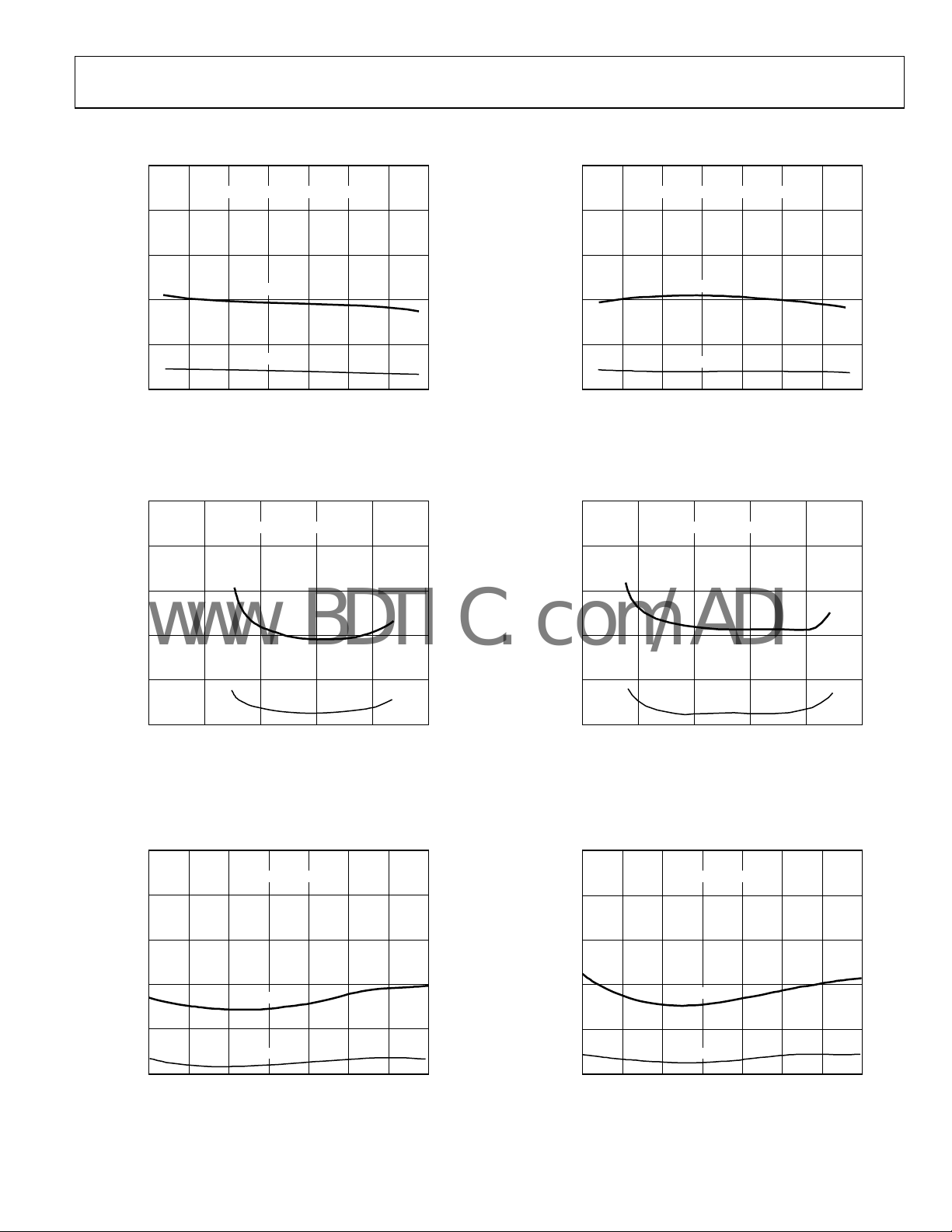
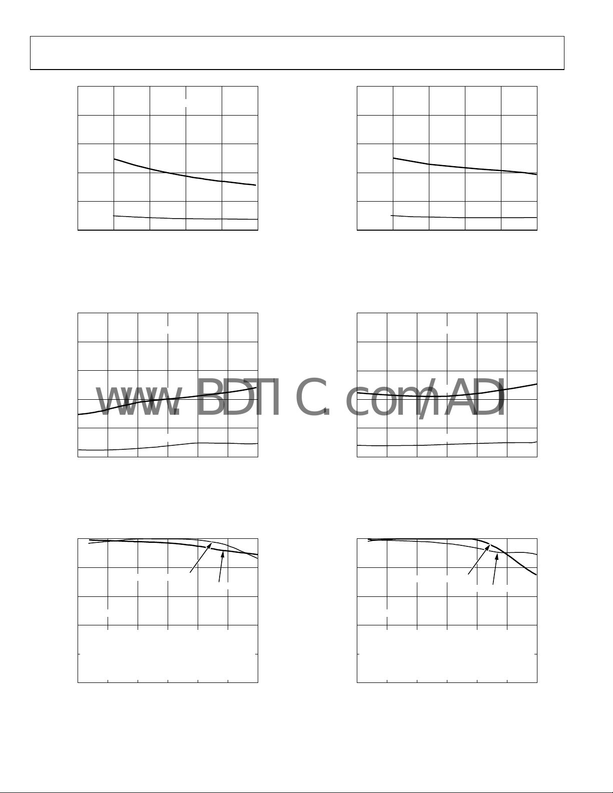
Figure 5. Jitter vs. V
100
80
60
JITTER (ps)
40
20
0
–2.0 –1.5 –0.5 0–1.0 0.5
Figure 6. Jitter vs. V
PK-PK
RMS
(V)
V
OH
1.5 Gbps, PRBS 23
OH
VEE = –3.3V (VIH– VIL = 800mV)
PK-PK
RMS
(V)
V
IN
1.5 Gbps, PRBS 23
IH
01074-005
01074-006
60
JITTER (ps)
40
20
0
0 –0.2 –0.6 –0.8 –1.0 –1.2–0.4 –1.4
Figure 8. Jitter vs. V
100
80
60
JITTER (ps)
40
20
0
–2.0 –1.5 –0.5 0–1.0 0.5
Figure 9. Jitter vs. V
PK-PK
RMS
V
(V)
OH
1.5 Gbps, PRBS 23
OH
VEE = –5V (VIH– VIL = 800mV)
PK-PK
RMS
V
(V)
IN
1.5 Gbps, PRBS 23
IH
01074-008
01074-009
100
80
60
JITTER (ps)
40
20
0
0.1 1.51.31.10.90.70.50.3
VEE = –3.3V
PK-PK
RMS
DATA RATE (Gbps)
Figure 7. Jitter vs. Data Rate, PRBS 23
01074-007
100
80
60
JITTER (ps)
40
20
0
0.1 1.51.31.10.90.70.50.3
Figure 10. Jitter vs. Data Rate, PRBS 23
Rev. A | Page 9 of 44
VEE = –5V
PK-PK
RMS
DATA RATE (Gbps)
01074-010
AD8150
www.BDTIC.com/ADI
100
80
VEE = –3.3V
100
VEE = –5V
80
60
JITTER (ps)
40
20
0
0 5 10 15 20 25
Figure 11. Jitter vs. I
100
80
60
JITTER (ps)
40
20
PK-PK
RMS
(mA)
I
OUT
1.5 Gbps, PRBS 23
OUT
VEE = –3.3V
PK-PK
RMS
01074-011
60
PK-PK
JITTER (ps)
40
20
0
0 5 10 15 20 25
Figure 14. Jitter vs. I
100
80
60
JITTER (ps)
40
20
RMS
(mA)
I
OUT
1.5 Gbps, PRBS 23
OUT
VEE = –5V
PK-PK
RMS
01074-014
0
–25 0 25 50 75 125100
TEMPERATURE (°C)
Figure 12. Jitter vs. Temperature 1.5 Gbps, PRBS 23
100
80
60
VEE = –3.3V
PERCENT
40
23
2
–1 PSEUDO-RANDOM BIT STREAM, ERROR-FREE AREA
ERROR-FREE PERCENTAGE VALUE WAS COMPUTED
20
(DATA_PERIOD – PPJITTER) × 100 / DATA_PERIOD
0
0 500 1000 1500
VOLTAGE (INNER EYE)
USING THE FOLLOWING FORMULA:
TIME DOMAIN
V
100 / V
INNER
INNER
VOLTAGE (INNER EYE)
DATA RATE (Mbps)
TIME DOMAIN
@500Mbps
Figure 13. AC Performance
01074-012
01074-013
0
–25 0 25 50 75 125100
TEMPERATURE (°C)
Figure 15. Jitter vs. Temperature 1.5 Gbps, PRBS 23
100
80
VOLTAGE (INNER EYE)
60
VEE = –5V
PERCENT
40
23
2
–1 PSEUDO-RANDOM BIT STREAM, ERROR-FREE AREA
ERROR-FREE PERCENTAGE VALUE WAS COMPUTED
20
0
0 500 1000 1500
USING THE FOLLOWING FORMULA:
(DATA_PERIOD – PPJITTER) × 100 / DATA_PERIOD
TIME DOMAIN
V
100 / V
INNER
VOLTAGE (INNER EYE)
INNER
DATA RATE (Mbps)
TIME DOMAIN
@500Mbps
Figure 16. AC Performance
01074-015
01074-016
Rev. A | Page 10 of 44
AD8150
www.BDTIC.com/ADI
100
150
80
60
40
FREQUENCY
20
0
560 580 620600 640 660 680 700 710
DELAY (ps)
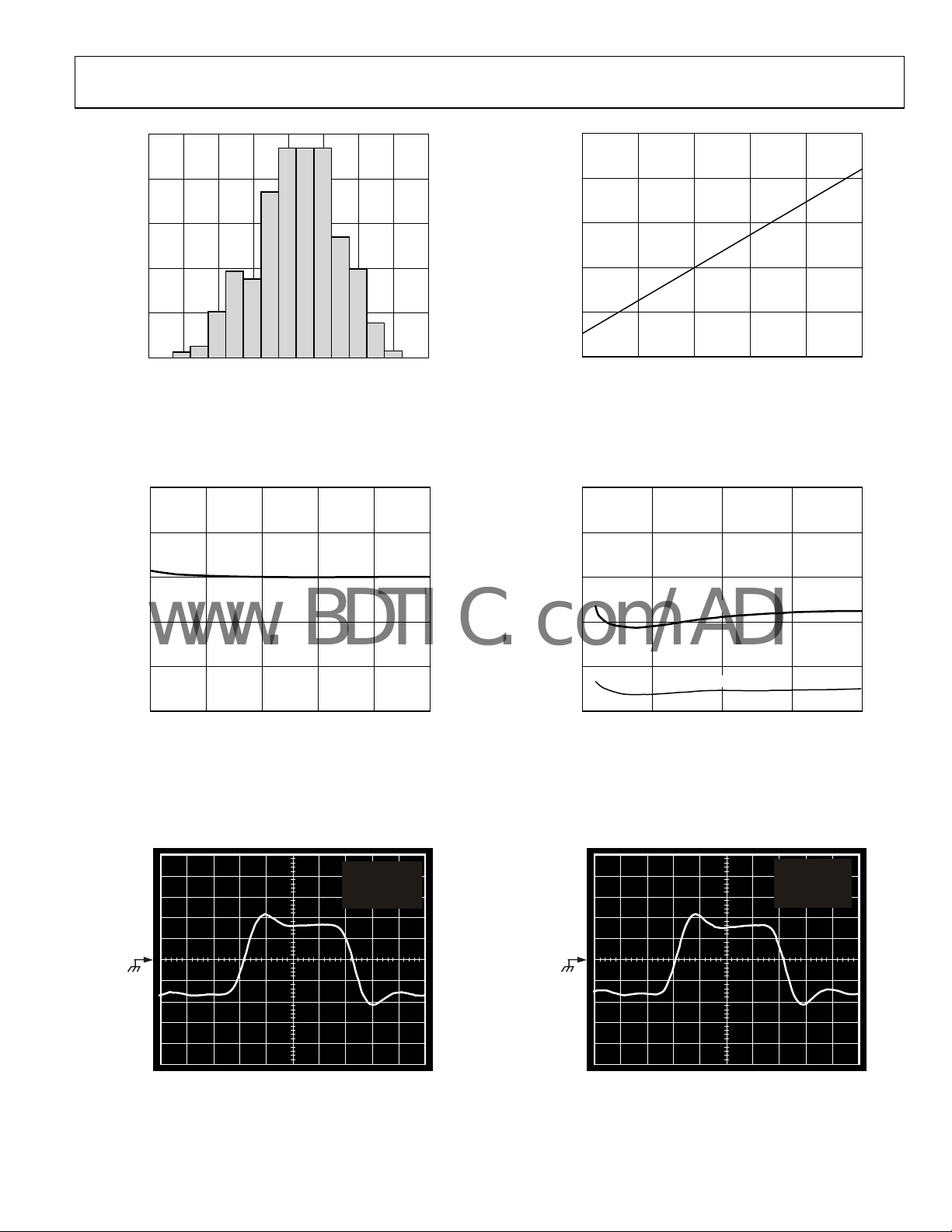
Figure 17. Variation in Channel-to-Channel Delay, All 561 Points
17.0
16.5
16.0
(mA)
OUT
I
15.5
01074-017
100
50
0
PROPAGTION DELAY (ps)
–50
–100
–25 0 25 50 75 100
TEMPERATURE (°C)
Figure 20. Propagation Delay, Normalized at 25°C vs. Temperature
100
80
60
PK-PK
JITTER (ps)
40
01074-020
15.0
14.5
–3.3 –3.6 –3.9 –4.2 –4.7 –5.0
Figure 18. I
1V
200mV/DIV
–1V
Figure 19. Rise/Fall Times, V
VEE (V)
vs. Supply, VEE
OUT
200ps/DIV
95.55 RISE
96.32 FALL
20% PROXIMAL
80% DISTAL
= −3.3 V
EE
01074-018
01074-019
20
0
3.0 3.5 4.0 4.5 5.0
SUPPLY VOLTAGE (V
RMS
CC
, VEE)
Figure 21. Jitter vs. Supply 1.5 Gbps, PRBS 23
1V
87.11 RISE
87.36 FALL
20% PROXIMAL
80% DISTAL
200mV/DIV
–1V
200ps/DIV
Figure 22. Rise/Fall Times, V
= −5 V
EE
01074-021
01074-022
Rev. A | Page 11 of 44
AD8150
www.BDTIC.com/ADI
500mV
500mV
100mV/DIV
–500mV
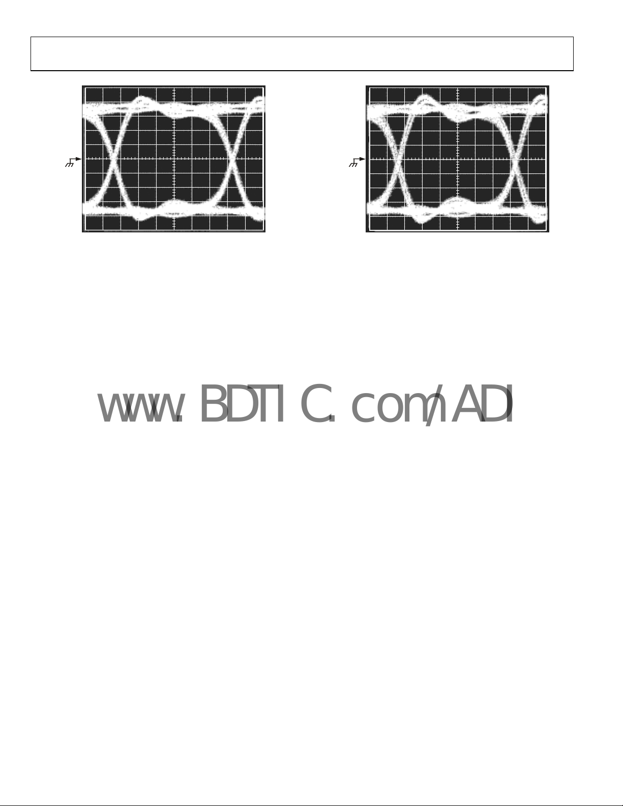
Figure 23. Eye Pattern, V
200ps/DIV
= −3.3 V, 1.5 Gbps PRBS 23
EE
01074-023
100mV/DIV
–500mV
Figure 24. Eye Pattern, V
100ps/DIV
= −5 V, 1.5 Gbps PRBS 23
EE
01074-025
Rev. A | Page 12 of 44

AD8150
V
www.BDTIC.com/ADI
TEST CIRCUIT
V
CCVCCVTT
TEKTRONIX
= 50Ω
R
1.65kΩ
HP8133A
PRBS
GENERATOR
1.65kΩ
= 0V, VEE = –3.3V OR –5V, VTT = –1.6V
CC
= 1.54kΩ, I
R
SET
INTRINSIC JITTER OF HP8133A AND TEKTRONIX 11801B = 3ps RMS, 17ps PK-PK
= 16mA, VOH = –0.8V, VOL = –1.8V
OUT
105Ω
V
EE
AD8150
P
IN OUT
N
V
EE
L
P
N
R
= 50Ω
L
V
TT
Figure 25. Eye Pattern Test Circuit
11801B
50Ω
SD22
SAMPLING
HEAD
50Ω
01074-024
Rev. A | Page 13 of 44

AD8150
www.BDTIC.com/ADI
CONTROL INTERFACE
CONTROL INTERFACE TRUTH TABLES
The following are truth tables for the control interface.
Table 4. Basic Control Functions
Control Pins
CS
RESET
0 X X X X Global Reset. Reset all second-rank enable bits to 0 (disable all outputs).
1 1 X X X
1 0 0 X X
1 0 X 0 X
1 0 X X 0
1 0 0 1 0
Table 5. Address Data Examples
Output Address Pins
A4 A3 A2 A1 A0 D6/E D5 D4 D3 D2 D1 D0 Function
0 0 0 0 0 X 0 0 0 0 0 0
1 0 0 0 0 X 1 0 0 0 0 0
<Binary Output Number1> 1 <Binary Input Number>
<Binary Output Number1> 0 X X X X X X Disable Output. Disable specified output (D6 = 0).
1 0 0 0 1 X <Binary Input Number>
1 0 0 1 0 X 1 0 0 0 0 1
1
The binary output number may also be the broadcast connection designator, 10001X.
WE RE UPDATE
MSB to LSB
Enable
Bit
Function
Control Disable. Ignore all logic (but the signal matrix still functions as programmed). D[6:0] are high
impedance.
Single Output Preprogram. Write input configuration data from Data Bus D[6:0] into first rank of
latches for the output selected by the Output Address Bus A[4:0].
Single Output Readback. Readback input configuration data from second rank of latches onto Data
Bus D[6:0] for the single output selected by the Output Address Bus A[4:0].
Global Update. Copy input configuration data from all 17 first-rank latches into second rank of
latches, updating signal matrix connections for all outputs.
Transparent Write and Update. It is possible to write data directly onto rank two. This simplifies logic
when synchronous signal matrix updating is not necessary.
Input Address Pins
MSB to LSB
Lower Address/Data Range. Connect Output 00
(A[4:0] = 00000) to Input 00 (D[5:0] = 000000).
Upper Address/Data Range. Connect Output 16
(A[4:0] = 10000) to Input 32 (D[5:0] = 100000).
Enable Output. Connect selected output (A[4:0] = 0 to 16) to
designated input (D[5:0] = 0 to 32) and enable output
(D6 = 1).
Broadcast Connection. Connect all 17 outputs to the same
designated input and set all 17 enable bits to the value of
D6. Readback is not possible with the broadcast address.
Reserved. Any address or data code greater or equal to these
are reserved for future expansion or factory testing.
Rev. A | Page 14 of 44
 Loading...