

Triple Differential Driver
–
www.BDTIC.com/ADI
FEATURES
Triple high speed differential driver
225 MHz, −3 dB large signal bandwidth
450 MHz, −3 dB small signal bandwidth
Easily drives 1.4 V p-p video signal into doubly terminated
100 Ω UT
1600 V/μs slew rate
Fixed internal gain of 2
Internal common-mode feedback network
Output balance error −60 dB @ 50 MHz
On-chip sync-on-common-mode circuitry
Output pull-down feature for line isolation
Differential input and output
Differential-to-differential or single-ended-to-differential
oper
High isolation between amplifiers: 80 dB @ 10 MHz
Low distortion: 64 dB SFDR @ 10 MHz on 5 V supply,
R
L, dm
Low offset: 3 mV typical output-referred on 5 V supply
Low power: 26.5 mA @ 5 V for three drivers and sync circuitry
Wide supply voltage range: +5 V to ±5 V
Available in space-saving packaging: 4 mm × 4 mm LFCSP
APPLICATIONS
Keyboard-video-mouse (KVM) networking
GENERAL DESCRIPTION
The AD8134 is a major advancement beyond using discrete
op amps for driving differential RGB signals over twisted pair
cable. The AD8134 is a triple, low cost differential or singleended input to differential output driver, and each amplifier has
a fixed gain of 2 to compensate for the attenuation of the line
termination resistors. The AD8134 is specifically designed for
RGB signals but can be used for any type of analog signals or
high speed data transmission. The AD8134 is capable of driving
either Category 5 (Cat-5) unshielded twisted pair (UTP) cable
or differential printed circuit board transmission lines with
minimal signal degradation.
A unique feature that allows the use
horizontal and vertical video sync signals over the three
common-mode channels with minimal electromagnetic
interference (EMI) radiation is included on-chip.
The outputs of the AD8134 can be set to a low voltage state that
al
lows easy differential multiplexing of multiple drivers on the
same twisted pair cable, when used with external series diodes.
Rev. A
Information furnished by Analog Devices is believed to be accurate and reliable. However, no
responsibility is assumed by Anal og Devices for its use, nor for any infringements of patents or ot her
rights of third parties that may result from its use. Specifications subject to change without notice. No
license is granted by implication or otherwise under any patent or patent rights of Analog Devices.
Trademarks and registered trademarks are the property of their respective owners.
P cable
ation
= 200 Ω
r to transmit balanced
With Sync-On-Common-Mode
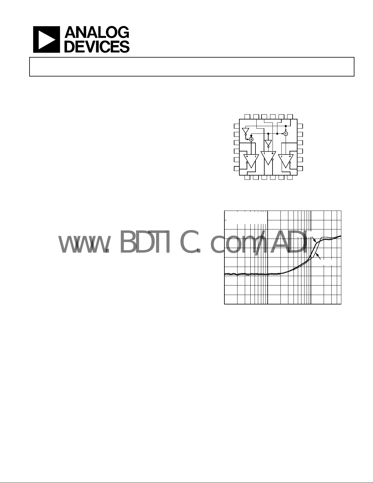
AD8134
FUNCTIONAL BLOCK DIAGRAM
(SYNC)
SYNC
S–
SYNC
VS+–IN G
24 23 22 21 20
AD8134
OPD
1
V
2
S–
–IN R
3
+IN R
4
V
S–
OUT R
0
ΔV
–10
ΔV
–20
–30
–40
–50
–60
–70
–80
OUTPUT BALANCE ERROR (dB)
–90
–100
1 10 100 500
R
5
6
7 8 9 10 11
+OUT R
= 2V p-p
OUT, dm
/ΔV
OUT, cm
S+
V
OUT, dm
Figure 2. Output Balance vs. Frequency
The AD8134 driver is a natural complement to the AD8143,
AD8129, and AD8130 differential receivers.
Manufactured on the Analog Devices next generation XFCB
b
ipolar process, the AD8134 has a large signal bandwidth of
225 MHz and a slew rate of 1600 V/μs. The AD8134 has an
internal common-mode feedback feature that provides output
gain and phase matching that is balanced to −60 dB at 50 MHz,
suppressing harmonics and reducing radiated EMI.
The AD8134 is available in a 24-lead LFCSP and can operate
o
ver the −40°C to +85°C extended industrial temperature range.
One Technology Way, P.O. Box 9106, Norwood, MA 02062-9106, U.S.A.
Tel: 781.329.4700 www.analog.com
Fax: 781.461.3113 © 2005 Analog Devices, Inc. All rights reserved.
V
+IN G
V
H
19
×2
G
B
12
S+
V
+OUT B
–OUT G
+OUT G
Figure 1.
VS = ±5V
FREQUENCY (MHz)
18
SYNC LEVEL
17
V
S+
16
–IN B
+IN B
15
V
14
S–
–OUT B
13
(SYNC)
VS = +5V
04770-001
04770-018

AD8134
www.BDTIC.com/ADI
TABLE OF CONTENTS
Features .............................................................................................. 1
Driving a Capacitive Load......................................................... 13
Applications....................................................................................... 1
General Description ......................................................................... 1
Functional Block Diagram .............................................................. 1
Revision History ............................................................................... 2
Specifications..................................................................................... 3
Absolute Maximum Ratings............................................................ 5
Thermal Resistance ...................................................................... 5
ESD Caution.................................................................................. 5
Pin Configuration and Function Descriptions............................. 6
Typical Performance Characteristics............................................. 7
Theory of Operation ...................................................................... 12
Definition of Terms.................................................................... 12
Analyzing an Application Circuit.............................................12
Closed-Loop Gain...................................................................... 12
Calculating an Application Circuit’s Input Impedance ......... 13
Output Pull-Down (OPD) ........................................................ 13
Sync-On-Common-Mode......................................................... 14
Applications..................................................................................... 15
Driving RGB Video Over Cat-5 Cable .................................... 15
How to Apply the Output Pull-Down Feature ....................... 16
KVM Networks........................................................................... 16
Video Sync-On-Common-Mode............................................. 16
Level-Shifting Sync Pulses on ±5 V Supplies.......................... 17
Layout and Power Supply Decoupling Considerations......... 18
Amplifier-to-Amplifier Isolation ............................................. 18
Exposed Paddle (EP).................................................................. 18
Outline Dimensions ....................................................................... 19
Ordering Guide .......................................................................... 19
Input Common-Mode Voltage Range in Single-Supply
Applications.................................................................................13
REVISION HISTORY
10/05—Rev. Sp0 to Rev. A
Changes to Features and General Description ............................. 1
Changes to Figure 32...................................................................... 14
Changes to Figure 33...................................................................... 15
Changes to Figure 34...................................................................... 17
Added Level-Shifting Sync Pulses on ±5 V Supplies Section ... 17
Changes to Ordering Guide.......................................................... 19
7/04—Revision Sp0: Initial Version
Rev. A | Page 2 of 20
AD8134
www.BDTIC.com/ADI
SPECIFICATIONS
VS = ±5 V, H
Table 1.
Parameter Conditions Min Typ Max Unit
DIFFERENTIAL INPUT PERFORMANCE
DYNAMIC PERFORMANCE
−3 dB Small Signal Bandwidth VO = 0.2 V p-p 450 MHz
−3 dB Large Signal Bandwidth VO = 2 V p-p 225 MHz
Bandwidth for 0.1 dB Flatness VO = 0.2 V p-p 60 MHz
V
Slew Rate VO = 2 V p-p, 25% to 75% 1600 V/μs
Settling Time to 0.1% VO = 2 V step 15 ns
Isolation Between Amplifiers
DIFFERENTIAL INPUT CHARACTERISTICS
Input Common-Mode Voltage Range −5 to +5 V
Input Resistance Differential 1.5 kΩ
Single-ended input 1.13 kΩ
Input Capacitance Differential 1 pF
DC CMRR ΔV
DIFFERENTIAL OUTPUT CHARACTERISTICS
Differential Signal Gain ΔV
Output Voltage Swing Each single-ended output VS− + 1.9 VS+ − 1.6 V
Output Offset Voltage −24 +4 +24 mV
Output Offset Drift T
Output Balance Error f = 50 MHz −60 dB
DC −70 −54 dB
Output Voltage Noise (RTO) f = 1 MHz 25 nV/√Hz
Output Short-Circuit Current 90 mA
COMMON-MODE SYNC PERFORMANCE
SYNC DYNAMIC PERFORMANCE
Slew Rate V
H
AND V
SYNC
Input Low Voltage VS− to −2.75 V
Input High Voltage −2.25 to VS+ V
SYNC LEVEL INPUT
Input Voltage Range For linear operation V
Setting to Achieve 0.5 V Pulse Levels VS− + 0.5 V
Gain to Red Common-Mode Output ΔV
Gain to Green Common-Mode Output ΔV
Gain to Blue Common-Mode Output ΔV
POWER SUPPLY
Operating Range +4.5 ±6 V
Quiescent Current 31 33 mA
PSRR ΔV
OUTPUT PULL-DOWN PERFORMANCE
OPD Input Low Voltage VS− to VS+ − 4.15 V
OPD Input High Voltage VS+ − 3.15 to VS+ V
OPD Input Bias Current 67 90 μA
OPD Assert Time 100 ns
OPD De-Assert Time 100 ns
Output Voltage When OPD Asserted Each output, OPD input @ VS+ VS− + 0.86 VS− + 0.90 V
SYNC
and V
SYNC
= VS−, R
= 200 Ω @ 25°C, unless otherwise noted. T
L, dm
= 2 V p-p 55 MHz
O
f = 10 MHz, between Amplifier R and
MIN
to T
= −40°C to +85°C.
MAX
80 dB
Amplifier G
/ΔV
, ΔV
OUT, dm
OUT, dm
to T
MIN
OUT, cm
INPUTS
SYNC
O, cm
O, cm
O, cm
OUT, dm
IN, cm
/ΔV
IN, dm
MAX
= −1 V to +1 V; 25% to 75% 1000 V/μs
/ΔV
SYNC LEVEL
/ΔV
SYNC LEVEL
/ΔV
SYNC LEVEL
/ΔVS; ΔVS = ±1V −54 −48 dB
= ±1 V −48 dB
IN, cm
, ΔV
= ±1 V 1.920 1.955 2.000 V/V
IN, dm
±30 μV/°C
0.95 1.02 1.07 V/V
1.91 2.04 2.14 V/V
0.95 1.02 1.07 V/V
Rev. A | Page 3 of 20
AD8134
www.BDTIC.com/ADI
VS+ = 5 V, VS− = 0 V, H
Table 2.
Parameter Conditions Min Typ Max Unit
DIFFERENTIAL INPUT PERFORMANCE
DYNAMIC PERFORMANCE
−3 dB Small Signal Bandwidth VO = 0.2 V p-p 400 MHz
−3 dB Large Signal Bandwidth VO = 2 V p-p 200 MHz
Bandwidth for 0.1 dB Flatness VO = 0.2 V p-p 50 MHz
Slew Rate VO = 2 V p-p, 25% to 75% 1400 V/μs
Settling Time to 0.1% VO = 2 V step 14 ns
Isolation Between Amplifiers
DIFFERENTIAL INPUT CHARACTERISTICS
Input Common-Mode Voltage Range 0 to 5 V
Input Resistance Differential 1.5 kΩ
Single-ended input 1.13 kΩ
Input Capacitance Differential 1 pF
DC CMRR ΔV
DIFFERENTIAL OUTPUT CHARACTERISTICS
Differential Signal Gain ΔV
Output Voltage Swing Each single-ended output VS− + 1.25 VS+ − 1.15 V
Output Offset Voltage −24 3 +24 mV
Output Offset Drift T
Output Balance Error f = 50 MHz −60 dB
DC −70 −54 dB
Output Voltage Noise f = 1 MHz 25 nV/√Hz
Output Short-Circuit Current 90 mA
COMMON-MODE SYNC PERFORMANCE
SYNC DYNAMIC PERFORMANCE
Slew Rate V
H
SYNC
AND V
INPUTS
SYNC
Input Low Voltage VS− to 1.10 V
Input High Voltage 1.40 to V
SYNC LEVEL INPUT
Input Voltage Range For linear operation V
Setting to Achieve 0.5 V Pulse Levels VS− + 0.5 V
Gain to Red Common-Mode Output ΔV
Gain to Green Common-Mode Output ΔV
Gain to Blue Common-Mode Output ΔV
POWER SUPPLY
Operating Range +4.5 ±6 V
Quiescent Current 26.5 27.5 mA
PSRR −54 −48 dB
OUTPUT PULL-DOWN PERFORMANCE
OPD Input Low Voltage VS− to VS+ − 3.85 V
OPD Input High Voltage VS+ − 2.85 to VS+ V
OPD Input Bias Current 63 80 μA
OPD Assert Time 100 ns
OPD De-Assert Time 100 ns
Output Voltage When OPD Asserted Each output, OPD input @ VS+ VS− + 0.79 VS− + 0.82 V
SYNC
and V
SYNC
= VS−, R
= 200 Ω @ 25°C, unless otherwise noted. T
L, dm
f = 10 MHz, between Amplifier R and
75 dB
MIN
to T
= −40°C to +85°C.
MAX
Amplifier G
/ΔV
, ΔV
OUT, dm
OUT, dm
MIN
OUT, cm
O, cm
O, cm
O, cm
IN, cm
/ΔV
IN, dm
to T
MAX
= −1 V to +1 V; 25% to 75% 700 V/μs
/ΔV
SYNC LEVEL
/ΔV
SYNC LEVEL
/ΔV
SYNC LEVEL
= ±1 V −48 dB
IN, cm
, ΔV
= ±1 V 1.920 1.955 2.000 V/V
IN, dm
±30 μV/°C
S+
0.97 1.02 1.06 V/V
1.94 2.03 2.10 V/V
0.96 1.02 1.05 V/V
V
Rev. A | Page 4 of 20
AD8134
www.BDTIC.com/ADI
ABSOLUTE MAXIMUM RATINGS
Table 3.
Parameter Rating
Supply Voltage 12 V
H
, V
SYNC
, Sync Level ±V
SYNC
S
Power Dissipation See Figure 3
Input Common-Mode Voltage ±V
S
Storage Temperature Range −65°C to +125°C
Operating Temperature Range −40°C to +85°C
Lead Temperature (Soldering 10 sec) 300°C
Junction Temperature 150°C
Stresses above those listed under Absolute Maximum Ratings
may cause permanent damage to the device. This is a stress
rating only; functional operation of the device at these or any
other conditions above those indicated in the operational
section of this specification is not implied. Exposure to absolute
maximum rating conditions for extended periods may affect
device reliability.
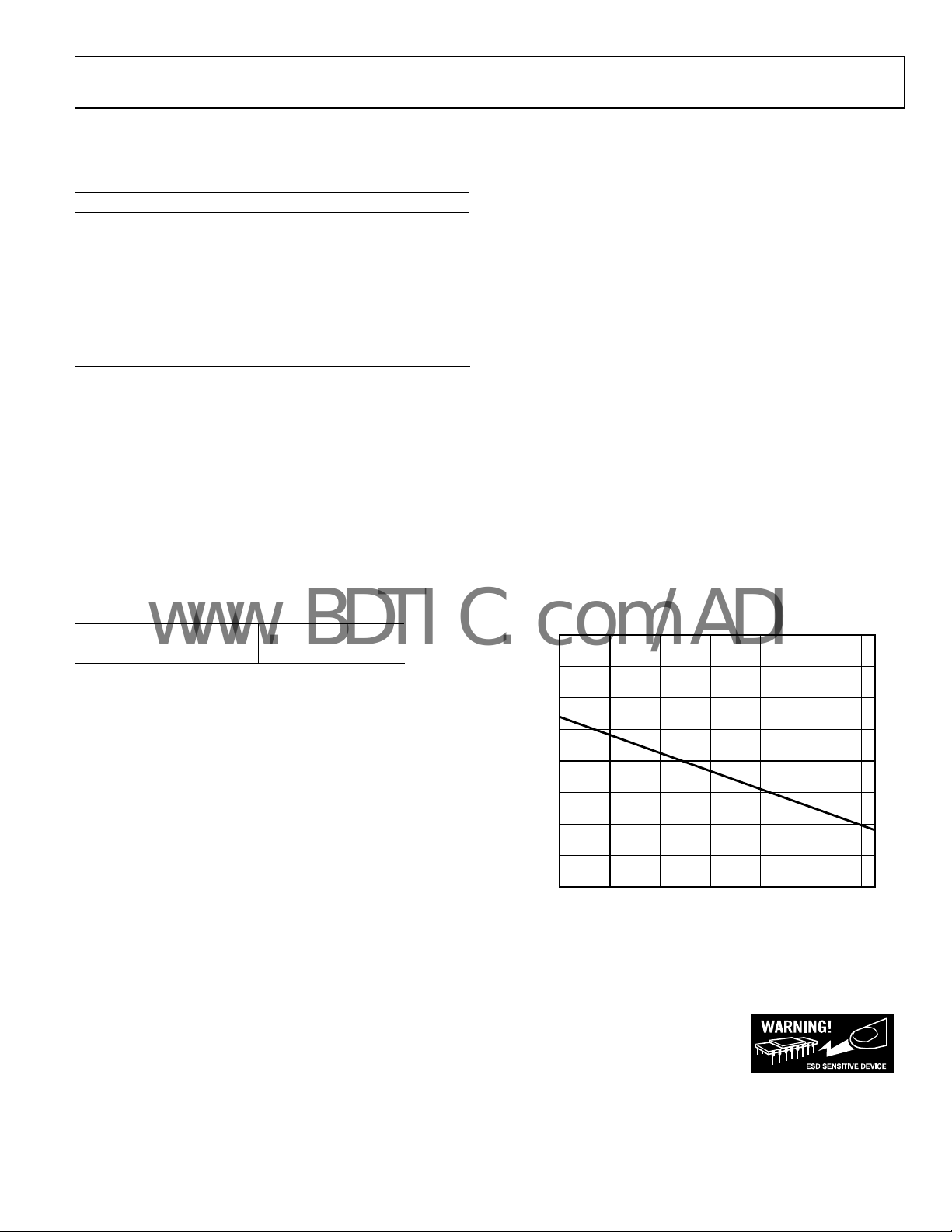
THERMAL RESISTANCE
θJA is specified for the worst-case conditions, that is, θJA is
specified for the device soldered in a circuit board in still air.
Table 4. Thermal Resistance with the Underside Pad
Thermall
Package Type/PCB Type θ
24-Lead LFCSP/4-Layer 70 °C/W
Maximum Power Dissipation
The maximum safe power dissipation in the AD8134 package is
limited by the associated rise in junction temperature (T
y Connected to a Copper Plane
JA
Unit
) on
J
The power dissipated in the package (P
quiescent power dissipation and the power dissipated in the
package due to the load drive for all outputs. The quiescent
power is the voltage between the supply pins (V
quiescent current (I
and common-mode currents flowing to the loads, as well as
currents flowing through the internal differential and commonmode feedback loops. The internal resistor tap used in the
common-mode feedback loop places a 4 kΩ differential load on
the output. RMS output voltages should be considered when
dealing with ac signals.
Airflow reduces θ
with the package leads from metal traces, through holes,
ground, and power planes reduce the θ
the underside of the package must be soldered to a pad on the
PCB surface that is thermally connected to a PCB plane to
achieve the specified θ
Figure 3 shows the maximum safe power dissipation in the
ackage vs. the ambient temperature for the 24-lead LFCSP
p
(70°C/W) on a JEDEC standard 4-layer board with the
underside paddle soldered to a pad that is thermally connected
to a PCB plane. θ
4.0
3.5
3.0
2.5
the die. At approximately 150°C, which is the glass transition
temperature, the plastic changes its properties. Even temporarily
exceeding this temperature limit can change the stresses that the
package exerts on the die, permanently shifting the parametric
performance of the AD8134. Exceeding a junction temperature
of 175°C for an extended period can result in changes in the
silicon devices potentially causing failure.
2.0
1.5
1.0
MAXIMUM POWER DISSIPATION (W)
0.5
0
–40 –20 0 20 40 60
Figure 3. Maximum Power Dissipation vs. Temperature for a 4-Layer Board
). The load current consists of differential
S
. In addition, more metal directly in contact
JA
.
JA
values are approximations.
JA
AMBIENT TEMPERATURE (°C)
) is the sum of the
D
) times the
S
. The exposed pad on
JA
LFCSP
80
04770-017
ESD CAUTION
ESD (electrostatic discharge) sensitive device. Electrostatic charges as high as 4000 V readily accumulate on
the human body and test equipment and can discharge without detection. Although this product features
proprietary ESD protection circuitry, permanent damage may occur on devices subjected to high energy
electrostatic discharges. Therefore, proper ESD precautions are recommended to avoid performance
degradation or loss of functionality.
Rev. A | Page 5 of 20
AD8134
–
www.BDTIC.com/ADI
PIN CONFIGURATION AND FUNCTION DESCRIPTIONS
(SYNC)
SYNC
S–
SYNC
+IN G
V
×2
G
–OUT G
+OUT G
AD8134
750Ω
V
H
19
18
SYNC LEVEL
(SYNC)
17
V
S+
16
–IN B
+IN B
15
B
S+
V
12
+OUT B
1.5kΩ
14
13
V
V
S–
–OUT B
+5V
S+
04770-001
0.1μF ON ALL
PINS
V
S+
VS+–IN G
24 23 22 21 20
AD8134
OPD
1
V
2
S–
–IN R
3
+IN R
4
V
OUT R
S–
R
5
6
7 8 9 10 11
V
+OUT R
S+
Figure 4. 24-Lead LFCSP
Table 5. Pin Function Descriptions
Pin No. Mnemonic Description
1 OPD Output Pull Down.
2, 5, 14, 21 V
S−
Negative Power Supply Voltage.
3 −IN R Inverting Input, Red Amplifier.
4 +IN R Noninverting Input, Red Amplifier.
6 −OUT R Negative Output, Red Amplifier.
7 +OUT R Positive Output, Red Amplifier.
8, 11, 17, 24 V
S+
Positive Power Supply Voltage.
9 +OUT G Positive Output, Green Amplifier.
10 −OUT G Negative Output, Green Amplifier.
12 +OUT B Positive Output, Blue Amplifier.
13 −OUT B Negative Output, Blue Amplifier.
15 +IN B Noninverting Input, Blue Amplifier.
16 −IN B Inverting Input, Blue Amplifier.
18 SYNC LEVEL
19 H
20 V
SYNC
SYNC
The voltage applied to this pin controls the amplitude of the sync pulses that are applied to
ommon-mode voltages.
the c
Horizontal Sync Pulse Input.
Vertical Sync Pulse Input.
22 +IN G Noninverting Input, Green Amplifier.
23 −IN G Inverting Input, Green Amplifier.
50Ω
V
TEST
TEST
SIGNAL
SOURCE
53.6Ω
53.6Ω
50Ω
750Ω
MIDSUPPLY
+
–
1.5kΩ
R
200Ω V
L, dm
V
S–
–5V
0.1μF ON ALL
V
PINS
S–
Figure 5. Basic Test Circuit
Rev. A | Page 6 of 20
–
OUT, dm
+
04770-034

AD8134
www.BDTIC.com/ADI
TYPICAL PERFORMANCE CHARACTERISTICS
VS = ±5 V, R
= 200, TA = 25°C, H
L, dm
9
6
SYNC
and V
+85°C
= VS−, unless otherwise noted.
SYNC
–40°C
+25°C
9
+85°C
6
–40°C
+25°C
3
GAIN (dB)
0
V
= 200mV p-p
OUT, dm
–3
1 10 100 1000
FREQUENCY (MHz)
Figure 6. Small Signal Frequency Response at Various Temperatures
9
6
VS = +5V
3
GAIN (dB)
0
–3
V
= 2V p-p
OUT, dm
–6
1 10 100 1000
FREQUENCY (MHz)
VS = ±5V
Figure 7. Large Signal Frequency Response for Various Power Supplies
04770-019
3
GAIN (dB)
0
V
= 2V p-p
OUT, dm
–3
1 10 100 1000
FREQUENCY (MHz)
04770-021
Figure 9. Large Signal Frequency Response at Various Temperatures
6.9
6.8
6.7
V
= 2V p-p
V
OUT, dm
OUT, dm
= 200mV p-p
04770-022
6.6
6.5
6.4
GAIN (dB)
6.3
6.2
6.1
6.0
04770-020
5.9
1 10 100 1000
FREQUENCY (MHz)
Figure 10. 0.1 dB Flatness
–30
–40
–50
–60
–70
–80
–90
DISTORTION (dBc)
–100
–110
–120
–130
0.1 1 10 100
R
L, dm
= 200Ω
FREQUENCY (MHz)
Figure 8. Second Harmonic Distortion at V
VS = +5V
V
OUT, dm
= 1000Ω
R
L, dm
= 5 V at Various Loads
S
= 2V p-p
04770-023
–30
–40
–50
–60
–70
DISTORTION (dBc)
–80
–90
–100
0.1 1 10 100
Figure 11. Third Harmonic Distortion at V
Rev. A | Page 7 of 20
R
= 200Ω
L, dm
FREQUENCY (MHz)
S
VS = +5V
= 2V p-p
V
OUT, dm
R
= 1000Ω
L, dm
= 5 V at Various Loads
04770-024

AD8134
www.BDTIC.com/ADI
–30
–40
–50
–60
–70
–80
–90
DISTORTION (dBc)
–100
–110
–120
0.1 1 10 100
R
= 200Ω
L, dm
FREQUENCY (MHz)
Figure 12. Second Harmonic Distortion at V
V
OUT, dm
= ±5 V at Various Loads
S
R
L, dm
= 2V p-p
= 1000Ω
04770-025
–30
–40
–50
R
= 200Ω
–60
–70
–80
–90
DISTORTION (dBc)
–100
–110
–120
–130
0.1 1 10 100
L, dm
FREQUENCY (MHz)
Figure 15. Third Harmonic Distortion at V
V
OUT, dm
R
L, dm
= ±5 V at Various Loads
S
= 2V p-p
= 1000Ω
04770-026
200
100
(mV)
OUT, dm
V
–50
–100
–200
VS = +5V
VS = ±5V
50
0
V
OUT, dm
5ns/DIV
= 200mV p-p
Figure 13. Small Signal Transient Response for Various Power Supply Voltages
10
8
6
4
2
0
–2
VOLTAGE (V)
–4
–6
–8
–10
2 × V
IN, dm
100ns/DIV
V
OUT, dm
Figure 14. Overdrive Recovery
V
= 2V p-p
VS = +5V
1.0
VS = ±5V
0.5
(V)
0
OUT, dm
V
–0.5
–1.0
04770-009
OUT, dm
5ns/DIV
04770-008
Figure 16. Large Signal Transient Response for Various Power Supply Voltages
V
IN, dm
250mV/DIV
+0.1%
SETTLING TIME ERROR
2mV/DIV
04770-014
t
= 0
10ns/DIV
–0.1%
04770-012
Figure 17. Settling Time (0.1%)
Rev. A | Page 8 of 20

AD8134
www.BDTIC.com/ADI
2
1
0
R
=
∞
L, dm
SINGLE-ENDED OUTPUT
–30
–35
–40
Δ
V
Δ
V
OUT, dm
IN, cm
/ΔV
IN, cm
= 200mV p-p
VS = +5V
–1
–2
VOLTAGE (V)
–3
–4
–5
Figure 18. Output Pull-Down Response
1000
100
NOISE (nV√Hz)
10
10 100 1k 10k 100k 1M 10M 100M
Figure 19. Output-Referred V
OUTPUT
PULL-DOWN
FREQUENCY (Hz)
100ns/DIV
V
oltage Noise vs. Frequency
ON
V
OUTN
04770-027
–45
–50
–55
COMMON-MODE REJECTION (dB)
–60
04770-013
–65
1 10 100 1000
Figure 21. Common-Mode Rejectio
10
ΔV
OUT, dm
0
–10
–20
–30
PSRR (dB)
–40
–50
–60
–70
0.1 1 10 100 1000
Figure 22. Power Supply Rejecti
FREQUENCY (MHz)
/ΔV
S
FREQUENCY (MHz)
n Ratio vs. Frequency
PSRR+
PSRR–
on Ratio vs. Frequency
VS = ±5V
04770-015
04770-029
0
Δ
V
Δ
V
–10
–20
–30
–40
–50
–60
–70
–80
OUTPUT BALANCE ERROR (dB)
–90
–100
1 10 100 500
OUT, dm
OUT, cm
= 2V p-p
/ΔV
OUT, dm
VS = ±5V
FREQUENCY (MHz)
Figure 20. Output Balance vs. Frequency
VS = +5V
ISOLATION (dB)
04770-028
Rev. A | Page 9 of 20
–40
RED TO GREEN
Δ
V
G/ΔV
OUT, dm
–50
–60
–70
–80
–90
–100
–110
1 10 100 1000
V
IN, dm
R
IN, dm
FREQUENCY (MHz)
= 200mV p-p
V
IN, dm
= 2V p-p
Figure 23. Amplifier-to-Amplifier Isolation vs. Frequency
04770-011

AD8134
www.BDTIC.com/ADI
–30
V
OUT, dm/VIN, dm WITH
–32
OUTPUT PULL-DOWN
–34
–36
–38
V
2V p-p
IN =
–40
–42
–44
–46
OUTPUT PULL-DOWN ISOLATION (dB)
–48
–50
0.1 1 10 100 1000
Figure 24. Output Pull-Down I
4.0
4.0
3.5
3.5
3.0
3.0
2.5
2.5
2.0
2.0
1.5
1.5
±5V SINGLE-ENDED OUTPUT VOLTAGE (V)
1.0
1.0
–40 –25 –5 15 35 55 75 85
FREQUENCY (MHz)
solation vs. Frequency
VS = ±5V
VS = +5V
TEMPERATURE (°C)
Figure 25. Positive Output Saturation Voltage vs. Temperature
40
VS = ±5V
35
5.0
4.5
4.0
3.5
04770-016
+5V SINGLE-ENDED OUTPUT VOLTAGE SWING (V)
04770-031
4.5
3.5
2.5
1.5
0.5
–0.5
–1.5
–2.5
–3.5
–4.5
±5V SINGLE-ENDED OUTPUT VOLTAGE SWING (V)
VS = +5V VS = ±5V
100 1000 10000
LOAD (Ω)
Figure 27. Output Saturation Voltage vs. Output Load
–1.0
R
L, dm
–1.5
–2.0
–2.5
–3.0
±5V SINGLE-ENDED OUTPUT VOLTAGE (V)
–3.5
–40 –25 –5 15 35 55 75 85
Figure 28. Negative Output Satur
VS = +5V
VS = ±5V
TEMPERATURE (°C)
ation Voltage vs. Temperature
= 200Ω
1.5
1.0
0.5
0
5
4
3
2
1
0
04770-033
+5V SINGLE-ENDED OUTPUT VOLTAGE SWING (V)
04770-032
+5V SINGLE-ENDED OUTPUT VOLTAGE SWING (V)
30
25
20
15
SUPPLY CURRENT (mA)
10
5
0
–40 –30 10–10 705030 85
VS = +5V
TEMPERATURE (°C)
04770-030
Figure 26. Power Supply Current vs. Temperature
Rev. A | Page 10 of 20

AD8134
www.BDTIC.com/ADI
3.5
3.0
2.5
2.0
1.5
OUTPUT AMPLITUDE (V)
1.0
RED
BLUE
GREEN
V
SYNC
VS = +5V
30
25
20
15
10
SYNC AMPLITUDE (V)
5
0.5
H
SYNC
5ns
0
Figure 29. Output Common-Mode Signals for Various Sync Pulse Inputs
0
04770-010
–5
Rev. A | Page 11 of 20

AD8134
+
V
www.BDTIC.com/ADI
THEORY OF OPERATION
Each differential driver in the AD8134 differs from a
conventional op amp in that it has two outputs whose voltages
move in opposite directions. Like an op amp, it relies on high
open-loop gain and negative feedback to force these outputs to
the desired voltages. The AD8134 drivers make it easy to
perform single-ended-to-differential conversion, commonmode level-shifting, and amplification of differential signals.
Previous differential drivers, both discrete and integrated
ns, are based on using two independent amplifiers and two
desig
independent feedback loops, one to control each of the outputs.
When these circuits are driven from a single-ended source, the
resulting outputs are typically not well balanced. Achieving a
balanced output has typically required exceptional matching of
the amplifiers and feedback networks.
DC common-mode level-shifting has also been difficult with
revious differential drivers. Level-shifting has required the use
p
of a third amplifier and feedback loop to control the output
common-mode level. Sometimes, the third amplifier has also
been used to attempt to correct an inherently unbalanced
circuit. Excellent performance over a wide frequency range has
proven difficult with this approach.
Each of the AD8134 drivers uses two feedback loops to
eparately control the differential and common-mode output
s
voltages. The differential feedback, set by the internal resistors,
controls the differential output voltage only. The internal
common-mode feedback loop controls the common-mode
output voltage only. This architecture makes it easy to
arbitrarily set the output common-mode level by simply
applying a voltage to the V
input. The output common-
OCM
mode voltage is forced, by internal common-mode feedback, to
equal the voltage applied to the V
differential output voltage. The V
input, without affecting the
OCM
inputs are not available to
OCM
the user but are internally connected to the sync-on-commonmode circuitry.
The AD8134 architecture results in outputs that are highly
alanced over a wide frequency range without requiring
b
external components or adjustments. The common-mode
feedback loop forces the signal component of the output
common-mode voltage to be zeroed. The result is nearly
perfectly balanced differential outputs of identical amplitude
that are exactly 180° apart in phase.
DEFINITION OF TERMS
Differential Voltage
Differential voltage refers to the difference between two node
v
oltages that are balanced with respect to each other. For
example, in
e
quivalently output differential mode voltage) is defined as
Figure 30, the output differential voltage (or
= (VOP − VON)
V
OUT, dm
Common-mode voltage refers to the average of two node
ltages with respect to a common reference. The output
vo
common-mode voltage is defined as
VV
)(
ONOP
V
=
,
cmOUT
2
Output Balance
Output balance is a measure of how well the differential output
ignals are matched in amplitude and how close they are to
s
exactly 180° apart in phase. Balance is easily determined by
placing a well-matched resistor divider between the differential
output voltage nodes and comparing the magnitude of the
signal at the divider’s midpoint with the magnitude of the
differential signal. By this definition, output balance error is the
magnitude of the change in output common-mode voltage
divided by the magnitude of the change in output differentialmode voltage in response to a differential input signal
V
Δ
cmOUT
,
ErrorBalanceOutput
=
V
Δ
dmOUT
,
ANALYZING AN APPLICATION CIRCUIT
The AD8134 uses high open-loop gain and negative feedback
to force its differential and common-mode output voltages to
minimize the differential and common-mode input error
voltages. The differential input error voltage is defined as the
voltage between the differential inputs labeled V
and VAN in
AP
Figure 30. For most purposes, this voltage can be assumed to be
zer
o. Similarly, the difference between the actual output
common-mode voltage and the voltage applied to V
can also
OCM
be assumed to be zero. Starting from these two assumptions,
any application circuit can be analyzed.
CLOSED-LOOP GAIN
The differential mode gain of the circuit in Figure 30 can be
described by
V
where R
+
IN, dm
OUT,dm
V
IN,dm
F
–
V
R
F
2==
R
G
= 1.5 kΩ and RG = 750 Ω nominally.
R
F
V
V
OCM
V
R
IP
IN
R
AP
G
V
AN
G
Figure 30. Circuit Definitions
R
F
R
L, dm
V
ON
V
OUT, dm
V
OP
04770-005
Rev. A | Page 12 of 20

AD8134
www.BDTIC.com/ADI
CALCULATING AN APPLICATION CIRCUIT’S INPUT IMPEDANCE
The effective input impedance of a circuit such as that in
Figure 30 at V
and VIN depends on whether the amplifier is
IP
being driven by a single-ended or differential signal source. For
balanced differential input signals, the differential input
impedance, R
R
IN,dm
In the case of a single-ended input signal (for example, if V
grounded and the input signal is applied to V
, between the inputs VIP and VIN is simply
IN, dm
= 2 × RG = 1.5 kΩ
), the input
IP
is
IN
impedance becomes
⎛
⎜
⎜
R
=
IN
⎜
⎜
⎝
R
G
1
R
−
()
2
⎞
⎟
⎟
=
⎟
F
⎟
RR
+×
FG
⎠
kΩ125.1
The circuit’s input impedance is effectively higher than it would
e for a conventional op amp connected as an inverter because
b
a fraction of the differential output voltage appears at the inputs
as a common-mode signal, partially bootstrapping the voltage
across the input resistor R
.
G
INPUT COMMON-MODE VOLTAGE RANGE IN SINGLE-SUPPLY APPLICATIONS
The inputs of the AD8134 are designed to facilitate levelshifting of ground referenced input signals on a single power
supply. For a single-ended input, this would imply, for example,
that the voltage at V
amplifier’s negative power supply voltage was also set to 0 V.
It is important to ensure that the common-mode voltage at the
mplifier inputs, V
a
Since voltages V
negative feedback, the amplifier’s input common-mode voltage
can be expressed as a single term, V
=
ACM
in Figure 30 would be 0 V when the
IN
and VAN, stays within its specified range.
AP
and VAN are driven to be essentially equal by
AP
. V
ACM
2
VVV+
ICMOCM
3
can be calculated as
ACM
DRIVING A CAPACITIVE LOAD
A purely capacitive load can react with the output impedance
of the AD8134 to reduce phase margin, resulting in high
frequency ringing in the pulse response. The best way to
minimize this effect is to place a small resistor in series with
each of the amplifier’s outputs to buffer the load capacitance.
OUTPUT PULL-DOWN (OPD)
The AD8134 has an OPD pin that when pulled high
significantly reduces the power consumed while simultaneously
pulling the outputs to within less than 1 V of V
with series diodes (see the Applications section). The equivalent
s
chematic of the output in the output pull-down state is shown
in
Figure 31. (The ESD diodes shown in Figure 31 are for ESD
rotection and are distinct from the series diodes used with the
p
output pull-down feature.) See Figure 18 and Figure 24 for the
o
utput pull-down transient and isolation performance. The
threshold levels for the OPD input pin are referenced to the
positive power supply and are listed in the
W
hen the OPD pin is pulled high, the AD8134 enters the
output pull-down state.
V
CC
ESD DIODE
PULL-DOWN
(OUTPUT IS
PULLED DOWN
WHEN SWITCH
IS CLOSED)
V
S–
Figure 31. Output Pull-Down
Equivalent Circuit
when used
S−
Specifications tables.
V
S+
V
OUT
ESD DIODE
04770-006
where V
that is,
is the common-mode voltage of the input signal,
ICM
VVV+
INIP
ICM
=
.
2
Rev. A | Page 13 of 20

AD8134
www.BDTIC.com/ADI
SYNC-ON-COMMON-MODE
The AD8134 drives RGB video signals over UTP cable. The
alance of the differential outputs is trimmed to ensure low
b
radiated energy from each of the twisted pairs. The commonmode outputs of each of the R, G, and B differential outputs
are set using the circuit in
orizontal and vertical sync pulses on the three common-mode
h
outputs in a way that also results in low radiated energy. For a
more detailed description of the sync scheme, see the
Applications section.
The sync-on-common-mode circuit generates a current based
n the SYNC LEVEL input pin (Pin 18). With SYNC LEVEL
o
input tied to V
at (V
+ VS−)/2. Using a resistor divider, a voltage can be
S+
, the common-mode output of all drivers is set
S−
applied between V
maximum deviation of the common-mode outputs from their
midsupply level. If, for instance, SYNC LEVEL − V
and the supply voltage is 5 V, then the common-mode outputs
fall within an envelope of 2.5 V ± 0.5 V. The state of each V
output based on the H
the equations defined in the Applications section.
Figure 32. This circuit embeds the
and SYNC LEVEL that determines the
S−
= 0.5 V
S−
SYNC
and V
inputs is determined by
SYNC
OUT, cm
On a single 5 V supply, the sync-on-common-mode circuit can
be used by directly applying the H
SYNC
and V
respective AD8134 inputs. The logic thresholds of the H
V
inputs are nominally set at (VS+ − VS−)/4, using a resistor
SYNC
signals to the
SYNC
SYNC
and
divider with an impedance of approximately 200 kΩ. This
allows the inputs to be driven beyond the rails without logic
inversion and maintains fast switching speeds. The robustness
of the H
SYNC
and V
inputs therefore allows them to be driven
SYNC
directly off the output of a computer video card without concern of
overdriving the inputs. The input path from H
SYNC
and V
SYNC
inputs to the switches in the current mode level-shifting circuit
are well matched to eliminate false switching transients. This
maximizes common-mode balance and minimizes radiated
energy.
The sync-on-common-mode circuit can be used with ±5 V
su
pplies, but in this case, the H
SYNC
and V
logic signals
SYNC
require level-shifting. Level-shifting details are provided in the
Applications section.
V
S+
MIRROR
V
SYNC
H
SYNC
SYNC LEVEL
H V
V
V
H
H
H V
V
S–
Figure 32. Sync-On-Common-Mode Simplified Circuit
HR
H
MIRROR
V
V
V
V
RR
RED V
OCM
GREEN V
OCM
BLUE V
OCM
RRR
R
04770-007
Rev. A | Page 14 of 20

AD8134
www.BDTIC.com/ADI
APPLICATIONS
V
1.5kΩ
+5V
S+
AD8134
0.1μF ON ALL
V
PINS
S+
DRIVING RGB VIDEO OVER CAT-5 CABLE
The AD8134 is a device whose foremost application is driving
RGB video signals over UTP cable in KVM networks. Singleended video signals are easily converted to differential signals
for transmission over the cable, and the internally fixed gain of
2 automatically compensates for the losses incurred by the
source and load terminations. The AD8134 can be used in all of
the typical KVM network topologies, including daisy-chained,
star, and point-to-point.
t
riple, single-ended-to-differential application in a daisy-
chained network when driven from a 75 Ω video source.
Figure 33 shows the AD8134 in a
75Ω
RED
VIDEO
SOURCE
75Ω
GREEN
VIDEO
SOURCE
75Ω
BLUE
VIDEO
SOURCE
OUTPUT
PULL-DOWN
80.6Ω
38.3Ω
80.6Ω
38.3Ω
80.6Ω
38.3Ω
750Ω
750Ω
750Ω
750Ω
750Ω
750Ω
OPD
1.5kΩ
1.5kΩ
1.5kΩ
1.5kΩ
1.5kΩ
V
R
G
B
S–
Figure 33. AD8134 in Single-Ended-to-Differential Application on S
49.9Ω
49.9Ω
49.9Ω
49.9Ω
49.9Ω
49.9Ω
UTP R
UTP G
UTP B
04770-002
ingle 5 V Supply (Sync Pulse Encoding Not Shown)
Rev. A | Page 15 of 20

AD8134
www.BDTIC.com/ADI
HOW TO APPLY THE OUTPUT PULL-DOWN FEATURE
The output pull-down feature, when used in conjunction with
series Schottky diodes, offers a convenient means to connect a
number of transmitters together to form a video network. The
OPD pin is a binary input that controls the state of the AD8134
outputs. Its binary input level is referenced to the most positive
power supply (see the
W
hen the OPD input is driven to its low state, the AD8134
output is enabled and operates in its normal fashion. In this
state, the sync-on-common-mode circuitry provides a
midsupply voltage and encoded sync pulses on the output
common-mode voltage. The midsupply voltage is used to
forward bias the series diodes, allowing the AD8134 to transmit
signals over the network. When the OPD input is driven to its
high state the outputs of the AD8134 are forced to a low voltage
irrespective of the levels on the sync inputs. This reverse-biases
the series diodes and presents a high impedance to the network.
This feature allows a three-state output to be realized that maintains
its high impedance state even when the AD8134 is not powered.
This condition can occur in KVM networks where the AD8134s do
not all reside in the same module, and where some modules in the
network are not powered.
It is recommended that the output pull-down feature only be
ed in conjunction with series diodes in such a way as to
us
ensure that the diodes are reverse-biased when the output pulldown feature is asserted because some loading conditions can
prevent the output voltage from being pulled all the way down.
Specifications section for the logic levels).
KVM NETWORKS
In daisy-chained KVM networks, the drivers are distributed along
one cable and a triple receiver is located at one end. Schottky
diodes in series with the driver outputs are biased such that the one
driver that is transmitting video signals has its diodes forwardbiased and the disabled drivers have their diodes reverse-biased.
The output common-mode voltage, set by the sync-on-commonmode circuitry, supplies the forward-biased voltage. When the
output pull-down feature is asserted, the differential outputs are
pulled to a low voltage, reverse-biasing the diodes.
In star networks, all cables radiate out from a central hub, which
ntains a triple receiver. The series diodes are all located at the
co
receiver in the star network. Only one ray of the star is
transmitting at a given time, and all others are isolated by
reverse-biased diodes. Diode biasing is controlled in the same
way as in the daisy-chained network.
In the daisy-chained and star networks that use diodes for
is
olation, return paths are required for the common-mode
currents that flow through the series diodes. A common-mode
tap can be implemented at each receiver by splitting the 100 Ω
termination resistor into two 50 Ω resistors in series. The diode
currents are routed from the tap between the 50 Ω resistors
back to the respective transmitters over one of the wires of the
fourth twisted pair in the UTP cable. Series resistors in the
common-mode path are generally required to set the desired
diode current.
In point-to-point networks, there is one transmitter and one
eceiver per cable, and the switching is generally implemented
r
with a crosspoint switch. In this case, there is no need to use
diodes or the output pull-down feature.
Diode and crosspoint switching are by no means the only type
o
f switching that can be used with the AD8134. Many other
types of mechanical, electromechanical, and electronic switches
can be used.
VIDEO SYNC-ON-COMMON-MODE
In computer video applications, the horizontal and vertical sync
signals are often separate from the video information
signals. For example, in typical computer monitor applications,
the red, green, and blue (RGB) color signals are transmitted
over separate cables, as are the vertical and horizontal sync
signals. When transmitting these types of video signals over
long distances on UTP cable, it is desirable to reduce the
required number of physical channels. One way to do this is to
encode the vertical and horizontal sync signals as weighted
sums and differences of the output common-mode signals. The
RGB color signals are each transmitted differentially over
separate physical channels. The fact that the differential and
common-mode signals are orthogonal allows the RGB color
and sync signals to be separated at the channel’s receiver.
Cat-5 cable contains four balanced twisted-pair physical
nnels that can support both differential and common-mode
cha
signals. Transmitting typical computer monitor video over this
cable can be accomplished by using three of the twisted pairs for
the RGB and sync signals and one wire of the fourth pair as a
return path for the Schottky diode bias currents. Each color is
transmitted differentially, one on each of the three pairs, and the
encoded sync signals are transmitted among the commonmode signals of each of the three pairs. To minimize EMI from
the sync signals, the common-mode signals on each of the three
pairs produced by the sync encoding scheme induce electric
and magnetic fields that for the most part cancel each other. A
conceptual block diagram of the sync encoding scheme is
presented in
s
cheme implemented internally, the user simply applies the
horizontal and vertical sync signals to the appropriate inputs.
(See the
w levels of the horizontal and vertical sync pulse voltages).
lo
Figure 34. Since the AD8134 has the sync encoding
Specifications tables for the definitions of the high and
Rev. A | Page 16 of 20

AD8134
2.04
4.52
2
2.12.22.32.42.92
2.52.62
G
www.BDTIC.com/ADI
+IN R
–IN R
V
SYNC
H
SYNC
SYNC LEVEL
+IN G
–IN G
+IN B
–IN B
OPD
V
WEIGHTING EQUATIONS:
OCM
RED V
=K(V
OCM
SYNC
OCM
OCM
2
=K(–2V
=K(V
2
2
SYNC
GREEN V
BLUE V
AD8134
– H
SYNC
SYNC
+ H
) + V
SYNC
) + V
MIDSUPPLY
MIDSUPPLY
) + V
MIDSUPPLY
×2
750Ω
750Ω
750Ω
750Ω
750Ω
750Ω
1.5kΩ
V
OCM
1.5kΩ
1.5kΩ
V
OCM
1.5kΩ
1.5kΩ
V
OCM
1.5kΩ
Figure 34. AD8134 Sync-On-Common-Mode Encoding Scheme
3.1
3.0
–OUT R
R
+OUT R
–OUT G
G
+OUT G
–OUT B
B
+OUT B
04770-003
5.0
3.5
3.0
1.5
1.0
0.5
Fi
gure 35. AD8134 Sync-On-Common-Mode Signals in Single 5 V Application
G
.8
.7
R
B
.0
.0
.5
H
SYNC
0
0.98 0.99 1.00 1.01 1.03 1.04 1.051.02 1.06 1.07
TIME (μs)
V
SYNC
04770-004
The transmitted common-mode sync signal magnitudes are
scaled by applying a dc voltage to the SYNC LEVEL input,
referenced to the negative supply. The difference between the
voltage applied to the SYNC LEVEL input and the negative
supply sets the peak deviation of the encoded sync signals about
the midsupply common-mode voltage. For example, with the
SYNC LEVEL input set at V
+ 500 mV, the deviation of the
S−
encoded sync pulses about the nominal midsupply commonmode voltage is typically ±500 mV. The equations in Figure 34
des
cribe how the V
SYNC
and H
signals are encoded on each
SYNC
color’s midsupply common-mode signal. In these equations, the
weights of the V
SYNC
and H
signals are ±1 (+1 for high, −1
SYNC
for low), and the constant K is equal to the peak deviation of the
encoded sync signals.
Figure 35 shows how the sync signals appear on each commonm
ode voltage in a single 5 V supply application when the
voltage applied to the SYNC LEVEL input is 500 mV. A typical
setting for the SYNC LEVEL voltage is 500 mV above the
negative supply.
Rev. A | Page 17 of 20
LEVEL-SHIFTING SYNC PULSES ON ±5 V SUPPLIES
The vertical and horizontal sync pulses received from a
computer video port are generally referenced to ground. When
using ±5 V supplies, these pulses must be level-shifted before
being applied to the negative-supply referenced V
inputs because these inputs are referenced to the negative
supply. The circuit shown in
lse level-shifting for a negative supply voltage of −5 V. The
pu
Figure 36 provides the proper sync
vertical and horizontal sync pulses each require a level-shift
circuit.
2N3906
ROUND-REFERENCED
SYNC PULSE
Figure 36. Level-Shifting Sync Puls
1kΩ
6.04kΩ 2.21kΩ
V
–
S
es on ±5 V Supplies
and H
SYNC
LEVEL-SHIFTED
SYNC PULSE
TO AD8134
SYNC
04770-035

AD8134
www.BDTIC.com/ADI
LAYOUT AND POWER SUPPLY DECOUPLING CONSIDERATIONS
Standard high speed PCB layout practices should be adhered to
when designing with the AD8134. A solid ground plane is
recommended and good wideband power supply decoupling
networks should be placed as close as possible to the supply
pins. Small surface-mount ceramic capacitors are recommended
for these networks, and tantalum capacitors are recommended
for bulk supply decoupling.
AMPLIFIER-TO-AMPLIFIER ISOLATION
The least amount of isolation between the three amplifiers
exists between Amplifier R and Amplifier G. This is therefore
viewed as the worst-case isolation and is what is reflected in the
Specifications tables and Typical Performance Characteristics.
R
efer to the basic test circuit in Figure 5 for test conditions.
EXPOSED PADDLE (EP)
The 24-lead LFCSP package has an exposed paddle on the
underside of its body. To achieve the specified thermal resistance,
it must have a good thermal connection to one of the PCB planes.
The exposed paddle must be soldered to a pad on top of the
board that is connected to an inner plane with several thermal
vias.
Rev. A | Page 18 of 20

AD8134
www.BDTIC.com/ADI
OUTLINE DIMENSIONS
0.60 MAX
19
18
EXPOSED
(BOTTOMVIEW)
13
12
PA D
24
6
7
1
2.50 REF
PIN 1
INDICATOR
*
2.45
2.30 SQ
2.15
0.23 MIN
PIN 1
INDICATOR
1.00
0.85
0.80
SEATING
PLANE
12° MAX
4.00
BSC SQ
TOP
VIEW
0.80 MAX
0.65 TYP
0.30
0.23
0.18
*
COMPLIANT TO JEDEC STANDARDS MO-220-VGGD-2
EXCEPT FOR EXPOSED PAD DIMENSION
Figure 37. 24-Lead Lead Frame Chip Scale Package [LFCSP_VQ]
4
3.75
BSC SQ
0.20 REF
mm × 4 mm Body, Very Thin Quad (CP-24-2)
Dimensions shown in millimeters
0.60 MAX
0.05 MAX
0.02 NOM
COPLANARITY
0.50
BSC
0.50
0.40
0.30
0.08
ORDERING GUIDE
Model Temperature Package Package Description Package Outline
AD8134ACP-R2 −40°C to +85°C 24-Lead LFCSP_VQ CP-24-2
AD8134ACP-REEL −40°C to +85°C 24-Lead LFCSP_VQ CP-24-2
AD8134ACP-REEL7 −40°C to +85°C 24-Lead LFCSP_VQ
AD8134ACPZ-R2
AD8134ACPZ-REEL
AD8134ACPZ-REEL7
1
Z = Pb-free part.
1
1
1
−40°C to +85°C 24-Lead LFCSP_VQ CP-24-2
−40°C to +85°C 24-Lead LFCSP_VQ CP-24-2
−40°C to +85°C 24-Lead LFCSP_VQ CP-24-2
CP-24-2
Rev. A | Page 19 of 20

AD8134
www.BDTIC.com/ADI
NOTES
© 2005 Analog Devices, Inc. All rights reserved. Trademarks and
registered trademarks are the property of their respective owners.
D04770-0-10/05(A)
T
Rev. A | Page 20 of 20
TTT
 Loading...