

Low Cost, High Speed
FEATURES
High speed
350 MHz −3 dB bandwidth
1200 V/µs slew rate
Resistor settable gain
Internal common-mode feedback to improve gain and
phase balance −68 dB @ 10 MHz
Separate input to set the common-mode output voltage
Low distortion: −99 dBc SFDR @ 5 MHz 800 Ω Load
Low power: 10.7 mA @ 5 V
Power supply range: +2.7 V to ±5.5 V
APPLICATIONS
Low power differential ADC drivers
Differential gain and differential filtering
Video line drivers
Differential in/out level shifting
Single-ended input to differential output drivers
Active transformers
GENERAL DESCRIPTION
The AD8132 is a low cost differential or single-ended input to
differential output amplifier with resistor settable gain. The
AD8132 is a major advancement over op amps for driving
differential input ADCs or for driving signals over long lines.
The AD8132 has a unique internal feedback feature that
provides output gain and phase matching balanced to −68 dB at
10 MHz, suppressing harmonics and reducing radiated EMI.
Manufactured using ADI’s next generation XFCB bipolar
process, the AD8132 has a −3 dB bandwidth of 350 MHz and
delivers a differential signal with −99 dBc SFDR at 5 MHz,
despite its low cost. The AD8132 eliminates the need for a
transformer with high performance ADCs, preserving the low
frequency and dc information. The common-mode level of the
differential output is adjustable by applying a voltage on the
pin, easily level shifting the input signals for driving
V
OCM
single-supply ADCs. Fast overload recovery preserves sampling
accuracy.
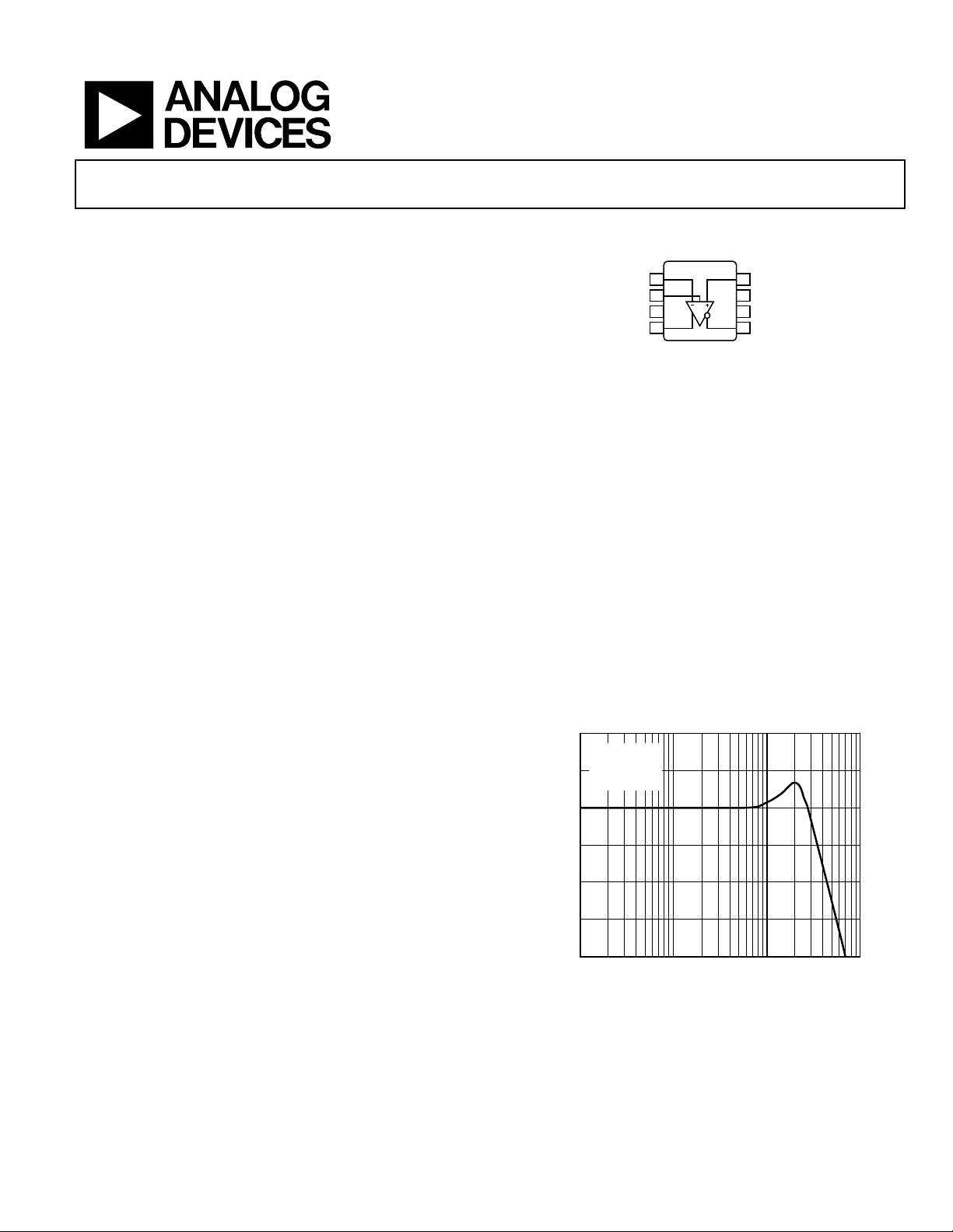
Differential Amplifier
AD8132
FUNCTIONAL BLOCK DIAGRAM
AD8132
–IN
1
2
V
OCM
V+
3
+OUT
4
NC = NO CONNECT
Figure 1.
The AD8132 can also be used as a differential driver for the
transmission of high speed signals over low cost twisted pair or
coaxial cables. The feedback network can be adjusted to boost
the high frequency components of the signal. The AD8132 can
be used for either analog or digital video signals or for other
high speed data transmission. The AD8132 is capable of driving
either cat3 or cat5 twisted pair or coaxial with minimal line
attenuation. The AD8132 has considerable cost and
performance improvements over discrete line driver solutions.
Differential signal processing reduces the effects of ground
noise that plagues ground referenced systems. The AD8132 can
be used for differential signal processing (gain and filtering)
throughout a signal chain, easily simplifying the conversion
between differential and single-ended components.
The AD8132 is available in both SOIC and MSOP packages for
operation over −40°C to +125°C temperatures.
6
VS = ±5V
G = +1
3
0
–3
GAIN (dB)
–6
–9
–12
= 2V p-p
V
O, dm
R
= 499Ω
L, dm
1
Figure 2. Large S ignal Frequenc y Respons e
10 100 1k
FREQUENCY (MHz)
+IN
8
NC
7
V–
6
–OUT
5
01035-001
01035-002
Rev. D
Information furnished by Analog Devices is believed to be accurate and reliable.
However, no responsibility is assumed by Analog Devices for its use, nor for any
infringements of patents or other rights of third parties that may result from its use.
Specifications subject to change without notice. No license is granted by implication
or otherwise under any patent or patent rights of Analog Devices. Trademarks and
registered trademarks are the property of their respective owners.
One Technology Way, P.O. Box 9106, Norwood, MA 02062-9106, U.S.A.
Tel: 781.329.4700
Fax: 781.326.8703 © 2004 Analog Devices, Inc. All rights reserved.
www.analog.com

AD8132
TABLE OF CONTENTS
Specifications..................................................................................... 3
±D
to ±OUT Specifications...................................................... 3
IN
V
to ±OUT Specifications ..................................................... 4
OCM
±D
to ±OUT Specifications...................................................... 5
IN
V
to ±OUT Specifications ..................................................... 6
OCM
±D
to ±OUT Specifications...................................................... 7
IN
V
to ±OUT Specifications ..................................................... 7
OCM
Absolute Maximum Ratings............................................................ 8
ESD Caution.................................................................................. 8
Pin Configuration and Function Descriptions............................. 9
Typical Performance Characteristics ...........................................10
Test Circuits..................................................................................... 19
Operational Description................................................................ 20
Definition of Terms.................................................................... 20
Basic Circuit Operation............................................................. 20
Theory of Operation ...................................................................... 21
General Usage of the AD8132................................................... 21
Resistorless Differential Amplifier (High Input Impedance
Inverting Amplifier)................................................................... 21
Varying β2 ................................................................................... 22
β1 = 0............................................................................................ 22
Estimating the Output Noise Voltage ...................................... 22
Calculating an Application Circuit’s Input Impedance......... 23
Input Common-Mode Voltage Range in Single-Supply
Applications ................................................................................ 23
Setting the Output Common-Mode Voltage .......................... 23
Driving a Capacitive Load......................................................... 23
Layout, Grounding, and Bypassing .............................................. 24
Circuits......................................................................................... 24
Applications..................................................................................... 25
A/D Driver .................................................................................. 25
Balanced Cable Driver............................................................... 25
Transmit Equalizer..................................................................... 26
Low-Pass Differential Filter...................................................... 26
High Common-Mode Output Impedance Amplifier............ 27
Full-Wave Rectifier .................................................................... 27
Outline Dimensions....................................................................... 29
Ordering Guide .......................................................................... 29
Other β2 = 1 Circuits ................................................................. 22
REVISION HISTORY
12/04—Rev. C to Rev. D.
Changes to the General Description.............................................. 1
Changes to the Specifications ......................................................... 2
Changes to the Absolute Maximum Ratings................................. 8
Updated the Outline Dimensions................................................. 29
Changes to the Ordering Guide.................................................... 29
Rev. D | Page 2 of 32
2/03—Rev. B to Rev. C.
Changes to SPECIFICATIONS .......................................................2
Addition to Estimating the Output Noise Voltage section ....... 15
Updated OUTLINE DIMENSIONS............................................ 21
1/02—Rev. A to Rev. B.
Edits to TRANSMITTER EQUALIZER section ...........................18

AD8132
SPECIFICATIONS
±DIN TO ±OUT SPECIFICATIONS
At 25°C, VS = ±5 V, V
= 499 Ω. Refer to Figure 56 and Figure 57 for test setup and label descriptions. All specifications refer to single-ended input and
R
G
differential outputs, unless otherwise noted.
Table 1.
Parameter Conditions Min Typ Max Unit
DYNAMIC PERFORMANCE
−3 dB Large Signal Bandwidth V
V
−3 dB Small Signal Bandwidth V
V
Bandwidth for 0.1 dB Flatness V
V
Slew Rate V
Settling Time 0.1%, V
Overdrive Recovery Time VIN = 5 V to 0 V Step, G = 2 5 ns
NOISE/HARMONIC PERFORMANCE
Second Harmonic V
V
V
Third Harmonic V
V
V
IMD 20 MHz, R
IP3 20 MHz, R
Input Voltage Noise (RTI) f = 0.1 MHz to 100 MHz 8
Input Current Noise f = 0.1 MHz to 100 MHz 1.8
Differential Gain Error NTSC, G = 2, R
Differential Phase Error NTSC, G = 2, R
INPUT CHARACTERISTICS
Offset Voltage (RTI) V
T
Input Bias Current 3 7 µA
Input Resistance Differential 12 MΩ
Common-Mode 3.5 MΩ
Input Capacitance 1 pF
Input Common-Mode Voltage −4 to +3 V
CMRR ∆V
OUTPUT CHARACTERISTICS
Output Voltage Swing Maximum ∆V
Output Current 70 mA
Output Balance Error ∆V
= 0 V, G = 1, R
OCM
= 499 Ω, RF = RG = 348 Ω, unless otherwise noted. For G = 2, R
L, dm
= 2 V p-p 300 350 MHz
OUT
= 2 V p-p, G = 2 190 MHz
OUT
= 0.2 V p-p 360 MHz
OUT
= 0.2 V p-p, G = 2 160 MHz
OUT
= 0.2 V p-p 90 MHz
OUT
= 0.2 V p-p, G = 2 50 MHz
OUT
= 2 V p-p 1000 1200 V/µs
OUT
= 2 V p-p 15 ns
OUT
= 2 V p-p, 1 MHz, R
OUT
= 2 V p-p, 5 MHz, R
OUT
= 2 V p-p, 20 MHz, R
OUT
= 2 V p-p, 1 MHz, R
OUT
= 2 V p-p, 5 MHz, R
OUT
= 2 V p-p, 20 MHz, R
OUT
= 800 Ω −76 dBc
L, dm
= 800 Ω 40 dBm
L, dm
L, dm
L, dm
OS, dm
MIN
OUT, dm
OUT, cm
= V
to T
/2; V
OUT, dm
Variation 10 µV/°C
MAX
/∆V
; ∆V
IN, cm
; Single-Ended Output −3.6 to +3.6 V
OUT
/∆V
OUT, dm
= 150 Ω 0.01 %
= 150 Ω 0.10 Degrees
; ∆V
= 800 Ω −96 dBc
L, dm
= 800 Ω −83 dBc
L, dm
= 800 Ω −73 dBc
L, dm
= 800 Ω −102 dBc
L, dm
= 800 Ω −98 dBc
L, dm
= 800 Ω −67 dBc
L, dm
= V
= V
DIN+
DIN−
= ±1 V; Resistors Matched to 0.01% −70 −60 dB
IN, cm
= 1 V −70 dB
OUT, dm
= 0 V ±1.0 ±3.5 mV
OCM
= 200 Ω, RF = 1000 Ω,
L, dm
nV/√
pA/√
Hz
Hz
Rev. D | Page 3 of 32

AD8132
V
TO ±OUT SPECIFICATIONS
OCM
At 25°C, VS = ±5 V, V
= 499 Ω. Refer to Figure 56 and Figure 57 for test setup and label descriptions. All specifications refer to single-ended input and
R
G
differential outputs, unless otherwise noted.
Table 2.
Parameter Conditions Min Typ Max Unit
DYNAMIC PERFORMANCE
−3 dB Bandwidth ∆V
Slew Rate ∆V
Input Voltage Noise (RTI) f = 0.1 MHz to 100 MHz 12
DC PERFORMANCE
Input Voltage Range ±3.6 V
Input Resistance 50 kΩ
Input Offset Voltage V
Input Bias Current 0.5 µA
V
CMRR ∆V
OCM
Gain ∆V
POWER SUPPLY
Operating Range ±1.35 ±5.5 V
Quiescent Current V
T
Power Supply Rejection Ratio ∆V
OPERATING TEMPERATURE RANGE −40 +125 °C
= 0 V, G = 1, R
OCM
= 499 Ω, RF = RG = 348 Ω, unless otherwise noted. For G = 2, R
L, dm
= 600 mV p-p 210 MHz
OCM
= −1 V to +1 V 400 V/µs
OCM
OS, cm
OUT, dm
OUT, cm
DIN+
MIN
OUT, dm
= V
= V
to T
; V
= V
= V
OUT, cm
DIN+
DIN−
/∆V
; ∆V
OCM
/∆V
OCM
= V
DIN−
Variation 16 µA/°C
MAX
= ±1 V; Resistors Matched to 0.01% −68 dB
OCM
; ∆V
= ±1 V 0.985 1 1.015 V/V
OCM
= 0 V 11 12 13 mA
OCM
= 0 V ±1.5 ±7 mV
OCM
/∆VS; ∆VS = ±1 V −70 −60 dB
= 200 Ω, RF = 1000 Ω,
L, dm
nV/√
Hz
Rev. D | Page 4 of 32

AD8132
±DIN TO ±OUT SPECIFICATIONS
At 25°C, VS = 5 V, V
= 499 Ω. Refer to Figure 56 and Figure 57 for test setup and label descriptions. All specifications refer to single-ended input and
R
G
differential outputs, unless otherwise noted.
Table 3.
Parameter Conditions Min Typ Max Unit
DYNAMIC PERFORMANCE
−3 dB Large Signal Bandwidth V
V
−3 dB Small Signal Bandwidth V
V
Bandwidth for 0.1 dB Flatness V
V
Slew Rate V
Settling Time 0.1%, V
Overdrive Recovery Time VIN = 2.5 V to 0 V Step, G = 2 5 ns
NOISE/HARMONIC PERFORMANCE
Second Harmonic V
V
V
Third Harmonic V
V
V
IMD 20 MHz, R
IP3 20 MHz, R
Input Voltage Noise (RTI) f = 0.1 MHz to 100 MHz 8
Input Current Noise f = 0.1 MHz to 100 MHz 1.8
Differential Gain Error NTSC, G = 2, R
Differential Phase Error NTSC, G = 2, R
INPUT CHARACTERISTICS
Offset Voltage (RTI) V
T
Input Bias Current 3 7 µA
Input Resistance Differential 10 MΩ
Common-Mode 3 MΩ
Input Capacitance 1 pF
Input Common-Mode Voltage 1 to 3 V
CMRR ∆V
OUTPUT CHARACTERISTICS
Output Voltage Swing Maximum ∆V
Output Current 50 mA
Output Balance Error ∆V
= 2.5 V, G = 1, R
OCM
= 499 Ω, RF = RG = 348 Ω, unless otherwise noted. For G = 2, R
L, dm
= 2 V p-p 250 300 MHz
OUT
= 2 V p-p, G = 2 180 MHz
OUT
= 0.2 V p-p 360 MHz
OUT
= 0.2 V p-p, G = 2 155 MHz
OUT
= 0.2 V p-p 65 MHz
OUT
= 0.2 V p-p, G = 2 50 MHz
OUT
= 2 V p-p 800 1000 V/µs
OUT
= 2 V p-p 20 ns
OUT
= 2 V p-p, 1 MHz, R
OUT
= 2 V p-p, 5 MHz, R
OUT
= 2 V p-p, 20 MHz, R
OUT
= 2 V p-p, 1 MHz, R
OUT
= 2 V p-p, 5 MHz, R
OUT
= 2 V p-p, 20 MHz, R
OUT
= 800 Ω −76 dBc
L, dm
= 800 Ω 40 dBm
L, dm
L, dm
L, dm
OS, dm
MIN
OUT, dm
OUT, cm
= V
to T
/2; V
OUT, dm
Variation 6 µV/°C
MAX
/∆V
; ∆V
IN, cm
; Single-Ended Output 1.0 to 4.0 V
OUT
/∆V
OUT, dm
= 150 Ω 0.025 %
= 150 Ω 0.15 Degree
; ∆V
= 800 Ω −97 dBc
L, dm
= 800 Ω −100 dBc
L, dm
= 800 Ω −74 dBc
L, dm
= 800 Ω −100 dBc
L, dm
= 800 Ω −99 dBc
L, dm
= 800 Ω −67 dBc
L, dm
= V
= V
DIN+
DIN−
= ±1 V; Resistors Matched to 0.01% −70 −60 dB
IN, cm
= 1 V −68 dB
OUT, dm
= 2.5 V ±1.0 ±3.5 mV
OCM
= 200 Ω, RF = 1000 Ω,
L, dm
nV/√
pA/√
Hz
Hz
Rev. D | Page 5 of 32

AD8132
V
TO ±OUT SPECIFICATIONS
OCM
At 25°C, VS = 5 V, V
= 499 Ω. Refer to Figure 56 and Figure 57 for test setup and label descriptions. All specifications refer to single-ended input and
R
G
differential outputs, unless otherwise noted.
Table 4.
Parameter Conditions Min Typ Max Unit
DYNAMIC PERFORMANCE
−3 dB Bandwidth ∆V
Slew Rate ∆V
Input Voltage Noise (RTI) f = 0.1 MHz to 100 MHz 12
DC PERFORMANCE
Input Voltage Range 1.0 to 3.7 V
Input Resistance 30 kΩ
Input Offset Voltage V
Input Bias Current 0.5 µA
V
CMRR ∆V
OCM
Gain ∆V
POWER SUPPLY
Operating Range 2.7 11 V
Quiescent Current V
T
Power Supply Rejection Ratio ∆V
OPERATING TEMPERATURE RANGE −40 +125 °C
= 2.5 V, G = 1, R
OCM
= 499 Ω, RF = RG = 348 Ω, unless otherwise noted. For G = 2, R
L, dm
= 600 mV p-p 210 MHz
OCM
= 1.5 V to 3.5 V 340 V/µs
OCM
OS, cm
OUT, dm
OUT, cm
DIN+
MIN
OUT, dm
= V
= V
to T
; V
= V
= V
OUT, cm
DIN+
DIN−
/∆V
; ∆V
OCM
/∆V
OCM
= V
DIN−
Variation 10 µA/°C
MAX
= 2.5 V ±1 V; Resistors Matched to 0.01% −66 dB
OCM
; ∆V
= 2.5 V ±1 V 0.985 1 1.015 V/V
OCM
= 2.5 V 9.4 10.7 12 mA
OCM
= 2.5 V ±5 ±11 mV
OCM
/∆VS; ∆VS = ±1 V −70 −60 dB
= 200 Ω, RF = 1000 Ω,
L, dm
nV/√
Hz
Rev. D | Page 6 of 32

AD8132
±DIN TO ±OUT SPECIFICATIONS
At 25°C, VS = 3 V, V
= 499 Ω. Refer to Figure 56 and Figure 57 for test setup and label descriptions. All specifications refer to single-ended input and
R
G
differential outputs, unless otherwise noted.
Table 5.
Parameter Conditions Min Typ Max Unit
DYNAMIC PERFORMANCE
−3 dB Large Signal Bandwidth V
V
−3 dB Small Signal Bandwidth V
V
Bandwidth for 0.1 dB Flatness V
V
NOISE/HARMONIC PERFORMANCE
Second Harmonic V
V
V
Third Harmonic V
V
V
INPUT CHARACTERISTICS
Offset Voltage (RTI) V
Input Bias Current 3 µA
CMRR ∆V
= 1.5 V, G = 1, R
OCM
= 499 Ω, RF = RG = 348 Ω unless otherwise noted. For G = 2, R
L, dm
= 1 V p-p 350 MHz
OUT
= 1 V p-p, G = 2 165 MHz
OUT
= 0.2 V p-p 350 MHz
OUT
= 0.2 V p-p, G = 2 150 MHz
OUT
= 0.2 V p-p 45 MHz
OUT
= 0.2 V p-p, G = 2 50 MHz
OUT
= 1 V p-p, 1 MHz, R
OUT
= 1 V p-p, 5 MHz, R
OUT
= 1 V p-p, 20 MHz, R
OUT
= 1 V p-p, 1 MHz, R
OUT
= 1 V p-p, 5 MHz, R
OUT
= 1 V p-p, 20 MHz, R
OUT
OS, dm
OUT, dm
= V
OUT, dm
/∆V
IN, cm
/2; V
; ∆V
= 800 Ω −100 dBc
L, dm
= 800 Ω −94 dBc
L, dm
= 800 Ω −77 dBc
L, dm
= 800 Ω −90 dBc
L, dm
= 800 Ω −85 dBc
L, dm
= 800 Ω −66 dBc
L, dm
= V
= V
DIN+
DIN−
= ±0.5 V; Resistors Matched to 0.01% −60 dB
IN, cm
= 1.5 V ±10 mV
OCM
= 200 Ω, RF = 1000 Ω,
L, dm
V
TO ±OUT SPECIFICATIONS
OCM
At 25°C, VS = 3 V, V
R
= 499 Ω. Refer to Figure 56 and Figure 57 for test setup and label descriptions. All specifications refer to single-ended input and
G
= 1.5 V, G = 1, R
OCM
= 499 Ω, RF = RG = 348 Ω unless otherwise noted. For G = 2, R
L, dm
= 200 Ω, RF = 1000 Ω,
L, dm
differential outputs, unless otherwise noted.
Table 6.
Parameter Conditions Min Typ Max Unit
DC PERFORMANCE
Input Offset Voltage V
Gain ∆V
OS, cm
OUT, cm
= V
OUT, cm
/∆V
OCM
; V
= V
= V
DIN+
DIN−
; ∆V
= ±0.5 V 1 V/V
OCM
= 1.5 V ±7 mV
OCM
POWER SUPPLY
Operating Range 2.7 11 V
Quiescent Current V
Power Supply Rejection Ratio ∆V
= V
= V
DIN+
DIN−
/∆VS; ∆VS = ±0.5 V −70 dB
OUT, dm
= 0 V 7.25 mA
OCM
OPERATING TEMPERATURE RANGE −40 +125 °C
Rev. D | Page 7 of 32
AD8132
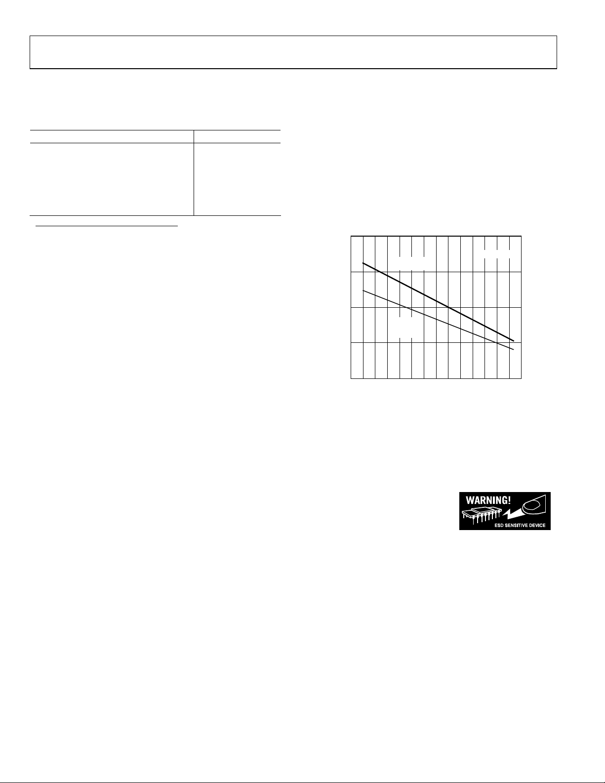
ABSOLUTE MAXIMUM RATINGS
Table 7.
Parameter Ratings
Supply Voltage ±5.5 V
V
Internal Power Dissipation 250 mW
Operating Temperature Range −40°C to +125°C
Storage Temperature Range −65°C to +150°C
Lead Temperature (Soldering 10 sec) 300°C
1
Thermal resistance measured on SEMI-standard, 4-layer board.
1
±VS
OCM
8-Lead SOIC: θ
8-Lead MSOP: θ
= 121°C/W
JA
= 142°C/W
JA
Stresses above those listed under absolute maximum ratings
may cause permanent damage to the device. This is a stress
rating only; functional operation of the device at these or any
other conditions above those listed in the operational section of
this specification is not implied. Exposure to Absolute
Maximum Ratings for extended periods may affect device
reliability.
2.0
1.5
1.0
0.5
MAXIMUM POWER DISSIPATION (W)
8-LEAD SOIC
PACKAGE
8-LEAD
MSOP
PACKAGE
TJ = 150°C
0
–40 –30
–50
Figure 3. Plot of Maximum Power Dissipation vs. Temperature
0 102030405060708090
–20 – 10
AMBIENT TEMPERATURE (°C)
ESD CAUTION
ESD (electrostatic discharge) sensitive device. Electrostatic charges as high as 4000 V readily accumulate
on the human body and test equipment and can discharge without detection. Although this product features
proprietary ESD protection circuitry, permanent damage may occur on devices subjected to high energy
electrostatic discharges. Therefore, proper ESD precautions are recommended to avoid performance
degradation or loss of functionality.
01035-003
Rev. D | Page 8 of 32
AD8132
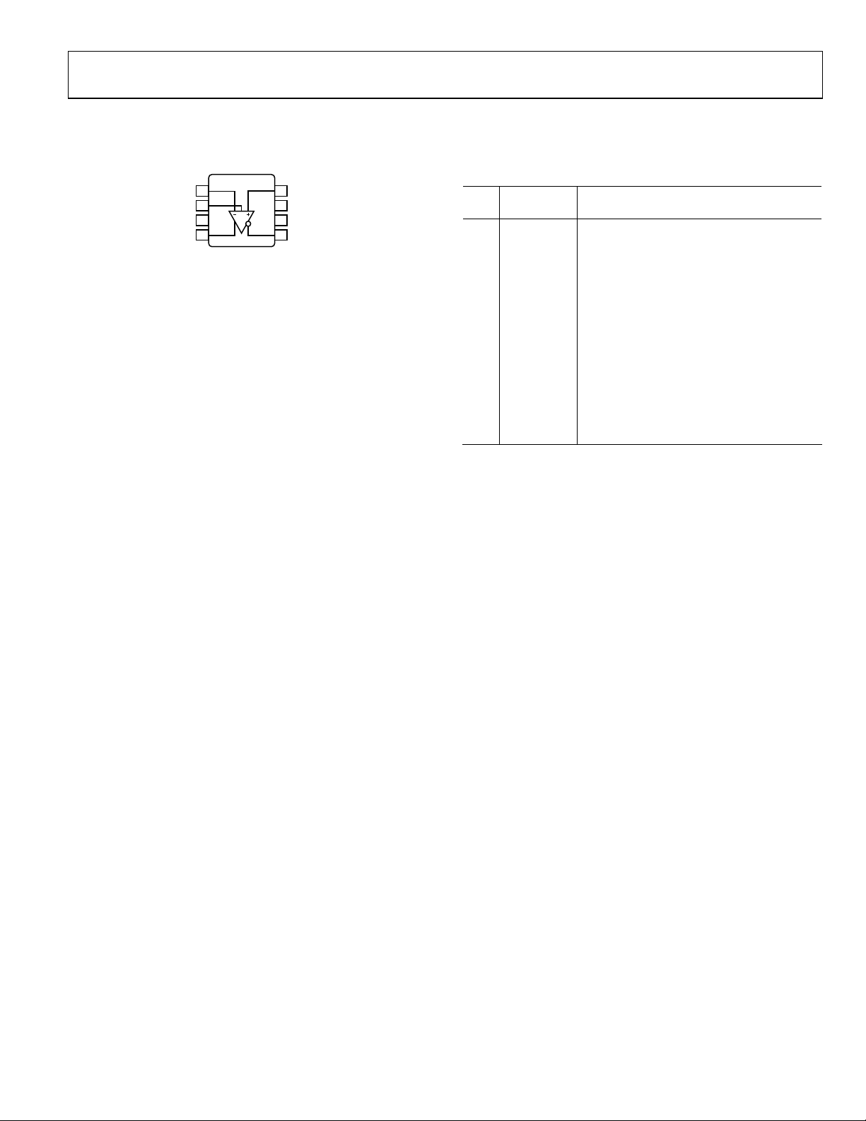
PIN CONFIGURATION AND FUNCTION DESCRIPTIONS
AD8132
–IN
1
V
2
OCM
V+
3
+OUT
4
NC = NO CONNECT
8
7
6
5
+IN
NC
V–
–OUT
01035-004
Figure 4. Pin Configuration
Table 8. Pin Function Descriptions
Pin
No.
Mnemonic Description
1 −IN Negative Input.
2 V
OCM
Voltage applied to this pin sets the
common-mode output voltage with
a ratio of 1:1. For example, 1 V dc on
sets the dc bias level on +OUT and
V
OCM
−OUT to 1 V.
3 V+ Positive Supply Voltage.
4 +OUT
5 −OUT
Positive Output. Note that the voltage at
is inverted at +OUT (see Figure 64).
−D
IN
Negative Output. Note that the voltage at
is inverted at −OUT (see Figure 64).
+D
IN
6 V− Negative Supply Voltage.
7 NC No Connect.
8 +IN Positive Input.
Rev. D | Page 9 of 32

AD8132
TYPICAL PERFORMANCE CHARACTERISTICS
2
1
0
–1
–2
GAIN (dB)
–3
G = +1
V
= 0.2V p-p
O, dm
= 499Ω
R
L, dm
–4
–5
1
10 100 1k
FREQUENCY (MHz)
Figure 5. Small Signal Frequency Respon se (See Figure 56)
VS = +3V
VS = ±5V
VS = +5V
01035-006
3
2
1
0
–1
GAIN (dB)
–2
G = +1
V
= 2V p-p FOR VS = ±5V, +5V
O, dm
–3
–4
–5
= 1V p-p FOR VS = +3V
V
O, dm
= 499Ω
R
L, dm
1 10 100 1k
FREQUENCY (MHz)
Figure 8. Large S ignal Frequenc y Respons e; C
VS = +3V
VS = +5V
VS = +3V
= 0 pF (See Figure 56)
F
VS = ±5V
01035-009
0.5
G = +1
0.4
V
= 0.2V p-p
O, dm
= 499Ω
R
L, dm
0.3
0.2
0.1
0
GAIN (dB)
–0.1
–0.2
–0.3
–0.4
–0.5
1 10 100 1k
FREQUENCY (MHz)
VS = ±5V
Figure 6. 0.1 dB Flatness vs. Frequency C
0.2
0.1
0
–0.1
–0.2
GAIN (dB)
–0.3
G = +1
V
= 0.2V p-p
O, dm
= 499Ω
R
–0.4
L, dm
–0.5
1 10 100 1k
VS = +3V
VS = ±5V
FREQUENCY (MHz)
Figure 7. 0.1 dB Flatness vs. Frequency C
VS = +3V
= 0 pF (See Figure 56)
F
VS = +5V
= 0.5 pF (See Figure 56)
F
VS = +5V
01035-007
01035-008
2
1
0
–1
–2
GAIN (dB)
G = +1
–3
–4
–5
= 2V p-p FOR VS = ±5V, +5V
V
O, dm
= 1V p-p FOR VS = +3V
V
O, dm
= 499Ω
R
L, dm
1 10 100 1k
VS = ±5V
FREQUENCY (MHz)
Figure 9. Large S ignal Frequenc y Respons e; C
3
2
1
0
–1
GAIN (dB)
–2
VS = ±5V
G = +1
–3
–4
–5
= 2V p-p
V
O, dm
= 499Ω
R
L, dm
1 10 100 1k
FREQUENCY (MHz)
VS = +3V
VS = +5V
VS = +3V
= 0.5 pF (See Figure 56)
F
+85°C
–40°C
+25°C
Figure 10. Large Signal Response vs. Temperature (See Figure 56)
01035-010
01035-011
Rev. D | Page 10 of 32

AD8132
3
2
1
0
–1
GAIN (dB)
–2
VS = ±5V
G = +1
–3
–4
–5
= 2V p-p
V
O, dm
= 499Ω
R
L, dm
1 10 100 1k
Figure 11. Large Signal Frequency Response vs. R
RF = 499Ω
RF = 348Ω
RF = 249Ω
FREQUENCY (MHz)
(See Figure 56)
F
01035-012
6.1
6.0
5.9
5.8
GAIN (dB)
5.7
VS = +3V, +5V, ±5V
G = +2
5.6
V
= 0.2V p-p
O, dm
= 200Ω
R
L, dm
5.5
1 10 100 1k
FREQUENCY (MHz)
Figure 14. 0.1 dB Flatness vs. Frequency (See Figure 57)
01035-016
100
10
IMPEDANCE (Ω)
1
0.1
1
FREQUENCY (MHz)
Figure 12. Closed-Loop Single-Ended Z
7
6
5
4
GAIN (dB)
3
G = +2
= 0.2V p-p
V
O, dm
= 200Ω
R
2
L, dm
VS = +5V
VS = ±5V
10 100
vs. Frequency; G = 1 (See Figure 56)
OUT
VS = ±5V, +5V
VS = +3V
01035-013
7
6
VS = +3V
5
4
GAIN (dB)
G = +2
= 2V p-p FOR
V
O, dm
= 1V p-p FOR
O, dm
= 200Ω
L, dm
= ±5V, +5V
S
= +3V
S
FREQUENCY (MHz)
V
3
V
V
R
2
1
1 10 100 1k
VS = +5V, ±5V
Figure 15. Large Signal Frequency Response (See Figure 57)
7
6
= 0.2V p-p
= 200Ω
RF = 1.0kΩ
RF = 499Ω
5
4
GAIN (dB)
VS = ±5V
3
G = +2
V
O, dm
R
L, dm
2
RF = 1.5kΩ
01035-017
1
1
10 100 1k
FREQUENCY (MHz)
Figure 13. Small Signal Frequency Response (See Figure 57)
01035-015
Rev. D | Page 11 of 32
1
1 10 100 1k
Figure 16. Small Signal Frequency Response vs. R
FREQUENCY (MHz)
(See Figure 57)
F
01035-018

AD8132
–
–
25
G = +10, RF = 4.99kΩ
20
G = +5, RF = 2.49kΩ
15
10
G = +2, RF = 1kΩ
5
G = +1, RF = 499Ω
GAIN (dB)
0
VS = ±5V
–5
V
= 2V p-p
O, dm
R
= 200Ω
L, dm
–10
R
= 499Ω
G
–15
1 10 100 1k
Figure 17. Large Signal Response for Various Gains (See Figure 58)
FREQUENCY (MHz)
01035-020
–30
R
= 800Ω
L, dm
= 2V p-p
V
O, dm
–40
–50
HD2 (VS = ±5V)
–60
–70
–80
DISTORTION (dBc)
–90
–100
–110
05
HD2 (VS = +5V)
20 30 4010
FREQUENCY (MHz)
HD3 (VS = +5V)
HD3 (VS = ±5V)
06070
01035-025
Figure 20. Harmonic Distortion vs. Frequency, G = 1 (See Figure 62)
25
VS = ±5V
–30
∆V
= 2V p-p
O, dm
∆V
/∆V
O, cm
–35
–40
–45
–50
–55
–60
RTI BALANCE ERROR (dB)
–65
–70
–75
1 10 100 1k
O, dm
G = +1
G = +2
FREQUENCY (MHz)
Figure 18. RTI Output Balance Error vs. Frequency (See Figure 59)
–40
R
= 800Ω
L, dm
V
= 1V p-p
O, dm
–50
HD3 (VS = 3V)
–60
HD2 (VS = 3V)
DISTORTION (dBc)
–70
–80
–90
HD2 (VS = 5V)
01035-022
–40
VS = 3V
= 800Ω
R
L, dm
–50
DISTORTION (dBc)
–100
–110
–60
–70
–80
–90
HD2 (F = 20MHz)
HD2 (F = 5MHz)
0.25 1.50 1.75
0.75 1.00 1.250.50
DIFFERENTIAL OUTPUT VOLTAGE (V p-p)
HD3 (F = 20MHz)
HD3 (F = 5MHz)
Figure 21. Harmonic Distortion vs.
Differential Output Voltage, G = 1 (See Figure 62)
40
VS = 5V
= 800Ω
R
L, dm
–50
HD3 (F = 20MHz)
HD2 (F = 20MHz)
HD2 (F = 5MHz)
DISTORTION (dBc)
–60
–70
–80
–90
01035-026
–100
–110
0 50607
HD3 (VS = 5V)
FREQUENCY (MHz)
Figure 19. Harmonic Distortion vs. Frequency, G = 1 (See Figure 62)
020 30 4010
01035-024
–100
–110
0
DIFFERENTIAL OUTPUT VOLTAGE (V p-p)
Figure 22. Harmonic Distortion vs.
231
HD3 (F = 5MHz)
01035-027
4
Differential Output Voltage, G = 1 (See Figure 62)
Rev. D | Page 12 of 32

AD8132
–
–
–
–40
DISTORTION (dBc)
–100
–110
–50
–60
–70
–80
–90
0
VS = ±5V
= 800Ω
R
L, dm
HD2 (F = 20MHz)
DIFFERENTIAL OUTPUT VOLTAGE (V p-p)
HD3 (F = 20MHz)
HD2 (F = 5MHz)
HD3 (F = 5MHz)
2341
Figure 23. Harmonic Distortion vs.
Differential Output Voltage, G = 1 (See Figure 62)
50
VS = 3V
= 1V p-p
V
O, dm
–60
–70
–80
–90
DISTORTION (dBc)
–100
–110
200 700 800
HD2 (F = 5MHz)
400 500 600300
Figure 24. Harmonic Distortion vs. R
HD3 (F = 20MHz)
HD2 (F = 20MHz)
HD3 (F = 5MHz)
R
(Ω)
LOAD
LOAD
5
900 1000
, G = 1 (See Figure 62)
6
01035-028
01035-029
–50
VS = ±5V
V
= 2V p-p
O, dm
–60
–70
–80
–90
DISTORTION (dBc)
–100
–110
200 700 800
HD2 (F = 5MHz)
400 500 600300
Figure 26. Harmonic Distortion vs. R
40
R
= 800Ω
L,dm
= 1V p-p
V
O, dm
–50
HD3 (VS = 3V)
–60
–70
–80
DISTORTION (dBc)
–90
–100
–110
10 20 300
HD2 (VS = 3V)
HD3 (VS = 5V)
FREQUENCY (MHz)
HD3 (F = 20MHz)
HD2 (F = 20MHz)
HD3 (F = 5MHz)
R
(Ω)
LOAD
LOAD
HD2 (VS = 5V)
40 50
900 1000
, G = 1 (See Figure 62)
60 70
Figure 27. Harmonic Distortion vs. Frequency, G = 2 (See Figure 63)
01035-031
01035-033
50
VS = 5V
V
= 2V p-p
O, dm
–60
–70
–80
–90
DISTORTION (dBc)
–100
–110
HD3 (F = 5MHz)
200 700 800
400 500 600300
Figure 25. Harmonic Distortion vs. R
R
LOAD
HD2 (F = 20MHz)
HD2 (F = 5MHz)
(Ω)
LOAD
HD3 (F = 20MHz)
900 1000
, G = 1 (See Figure 62)
01035-030
Rev. D | Page 13 of 32
DISTORTION (dBc)
–100
–20
–30
–40
–50
–60
–70
–80
–90
R
= 800Ω
L, dm
= 4V p-p
V
O,dm
HD2 (VS = +5V)
HD2 (VS = ±5V)
10 20 300
FREQUENCY (MHz)
HD3 (VS = +5V)
HD3 (VS = ±5V)
40 50
60 70
80
Figure 28. Harmonic Distortion vs. Frequency, G = 2 (See Figure 63)
01035-034

AD8132
–
40
–50
–60
–70
–80
–90
DISTORTION (dBc)
–100
–110
–120
–40
–50
–60
–70
–80
DISTORTION (dBc)
–90
–100
–110
–50
–60
–70
–80
VS = 5V
= 800Ω
R
L, dm
HD3 (F = 5MHz)
103
DIFFERENTIAL OUTPUT VOLTAGE (V p-p)
HD3 (F = 20MHz)
HD2 (F = 20MHz)
HD2 (F = 5MHz)
2
Figure 29. Harmonic Distortion vs.
Differential Output Voltage, G = 2 (See Figure 63)
VS = 5V
= 800Ω
R
L, dm
HD2 (F = 5MHz)
103
2
DIFFERENTIAL OUTPUT VOLTAGE (V p-p)
HD3 (F = 20MHz)
HD2 (F = 20MHz)
HD3 (F = 5MHz)
4
56
Figure 30. Harmonic Distortion vs.
Differential Output Voltage, G = 2 (See Figure 63)
VS = 5V
V
O, dm
= 2V p-p
HD3 (F = 20MHz)
HD2 (F = 20MHz)
4
01035-035
01035-036
DISTORTION (dBc)
–100
–110
–50
–60
–70
–80
–90
VS = ±5V
= 2V p-p
V
O, dm
HD2 (F = 5MHz)
HD3 (F = 5MHz)
300200 500
400
R
LOAD
Figure 32. Harmonic Distortion vs. R
10
fC = 20MHz
0
= ±5V
V
S
= 800Ω
R
L, dm
–10
–20
])
Ω
–30
–40
–50
(dBm [Re: 50
OUT
–60
P
–70
–80
–90
19.5
FREQUENCY (MHz)
Figure 33. Intermodulation Distortion, G = 1
45
40
])
Ω
35
30
HD3 (F = 20MHz)
HD2 (F = 20MHz)
600
700 800
(Ω)
, G = 2 (See Figure 63)
LOAD
20.0 20.5
VS = ±5V, +5V
= 800Ω
R
L, dm
900 1000
01035-038
01035-039
DISTORTION (dBc)
–100
–110
–90
300200 500
HD2 (F = 5MHz)
400
HD3 (F = 5MHz)
R
LOAD
Figure 31. Harmonic Distortion vs. R
700 800
600
(Ω)
, G = 2 (See Figure 63)
LOAD
900 1000
01035-037
25
INTERCEPT (dBm [Re: 50
20
15
010 70
20 30 40 50 60
FREQUENCY (MHz)
Figure 34. Third-Order Intercept vs. Frequency, G = 1
01035-040
Rev. D | Page 14 of 32

AD8132
VS = ±5V, +5V, +3V
40mV 5ns
Figure 35. Small Signal Transient Response, G = 1
CF = 0pF
CF = 0.5pF
VS = 3V
V
O, dm
= 1.5V p-p
01035-041
CF = 0pF
CF = 0.5pF
400mV 5ns
VS = ±5V
V
= 2V p-p
O,dm
Figure 38. Large Signal Transient Response, G = 1
V
O, dm
V
–OUT
V
+OUT
01035-044
300mV 5ns
Figure 36. Large Signal Transient Response, G = 1
CF = 0pF
CF = 0.5pF
400mV 5ns
VS = 5V
V
O, dm
= 2V p-p
Figure 37. Large Signal Transient Response, G = 1
01035-042
01035-043
V
+DIN
1V 5ns
Figure 39. Large Signal Transient Response, G = 1
VS = ±5V, +5V, +3V
40mV 5ns
Figure 40. Small Signal Transient Response, G = 2
01035-045
01035-046
Rev. D | Page 15 of 32

AD8132
VS = 3V
300mV 5ns
Figure 41. Large Signal Transient Response, G = 2
VS = +5V, ±5V
01035-047
VS = ±5V
G = +1
V
O, dm
R
L, dm
0.1%/DIV
2mV 5ns
0 5 10 15 20 25 30 35 40
5ns/DIV
Figure 44. 0.1% Settling Time
CL = 0pF
CL = 5pF
CL = 20pF
= 2V p-p
= 499Ω
01035-050
400mV 5ns
Figure 42. Large Signal Transient Response, G = 2
VS = ±5V
V
O, dm
V
–OUT
V
+OUT
V
+DIN
1V 5ns
Figure 43. Large Signal Transient Response, G = 2
01035-048
01035-049
400mV
Figure 45. Large Signal Transient Response
for Various Capacitor Loads (See Figure 60)
0
∆
V
O, dm
∆
–10
–20
–30
–40
–50
PSRR (dB)
–60
–70
–80
–90
V
S
+PSRR (VS =±5V, +5V)
–PSRR (V
0.1 1 10 100
=±5V)
S
FREQUENCY (MHz)
Figure 46. PSRR v s. Frequency
–PSRR
5ns
+PSRR
01035-052
01035-053
1k
Rev. D | Page 16 of 32

AD8132
–
–30
20
VS = ±5V
= 2V p-p
V
IN, cm
–10
–20
∆V
∆V
O, dm
∆V
OCM
= 600mV p-p
OCM
–40
–50
CMRR (dB)
–60
–70
–80
1 10 100 1000
∆V
O, cm
∆V
IN, cm
∆V
O, dm
∆V
IN, cm
FREQUENCY (MHz)
Figure 47. CMRR vs. Fre quency ( See Figure 61)
6
∆V
O,cm
∆V
OCM
3
0
∆V
–3
GAIN (dB)
–6
OCM
V
–9
–12
–15
1 10 100 1000
OCM
FREQUENCY (MHz)
Figure 48. V
∆V
= 2V p-p
Gain Response
OCM
OCM
VS = ±5V
= 600mV p-p
01035-055
01035-056
–30
∆V
= 2V p-p
–40
CMRR (dB)
–50
OCM
V
–60
–70
–80
1 10 100 1000
Figure 50. V
1k
100
10
INPUT VOLTAGE NOISE (nV/ Hz)
1
10
100 1k 10k 100k 1M 10M
FREQUENCY (MHz)
CMRR vs. Frequency
OCM
FREQUENCY (Hz)
OCM
8nV/ Hz
Figure 51. Input Voltage No ise vs. Frequency
100M
01035-058
01035-059
VS = ±5V
= –1V TO +1V
V
OCM
V
O, cm
400mV 5ns
Figure 49. V
Transient Response
OCM
01035-057
Rev. D | Page 17 of 32
1k
100
10
INPUT CURRENT NOISE (pA/ Hz)
1
10
1.8pA/ Hz
100 1k 10k 100k 1M 10M 100M
FREQUENCY (Hz)
Figure 52. Input Current Noise vs. Frequency
01035-060

AD8132
V
O, dm
V
(0.5V/DIV)
(1V/DIV)
IN, sm
–0.5
–1.0
0
VS = +5V
VS = 5V
= 2.5V STEP
V
IN
G = +2
= 1kΩ
R
F
= 200Ω
R
L, dm
5ns
Figure 53. Overdrive Recovery
15
13
VS = ±5V
11
VS = +5V
9
SUPPLY CURRENT (mA)
7
5
–50 –30 90
–10 10 30 50 70
TEMPERATURE (°C)
Figure 54. Quiescent Current vs. Temperature
01035-061
01035-062
–1.5
–2.0
DIFFERENTIAL OUTPUT OFFSET (mV)
–2.5
–40 –20 100
VS = ±5V
020406080
TEMPERATURE (°C)
01035-063
Figure 55. Differential Offset Voltage vs. Temperature
Rev. D | Page 18 of 32

AD8132
Ω
Ω
TEST CIRCUITS
348Ω
R
F
R
L
R
L
R
F
= 498Ω)
L, dm
L, dm
24.9Ω
C
L
= 200Ω)
453Ω
01035-021
C
F
348Ω
348Ω
49.9Ω
0.1µF
348Ω
24.9Ω
348Ω
C
F
Figure 56. Basic Test Circuit, G = 1
1000Ω
499Ω
49.9Ω
0.1µF
499Ω
200Ω
01035-005
R
G
49.9Ω
0.1µF
R
G
24.9Ω
G = +1: RF = RG = 348Ω, RL = 249Ω (R
G = +2: R
= 1000Ω, RG = 499Ω, RL = 100Ω (R
F
Figure 59. Test Circuit for Output Balance
348Ω
49.9Ω
0.1µF
499Ω
24.9Ω
1000Ω
Figure 57. Basic Test Circuit, G = 2
R
F
499Ω
49.9Ω
24.9Ω
0.1µF
499Ω
R
F
200Ω
Figure 58. Test Circuit for Various Gains
01035-014
01035-019
348Ω
24.9Ω
Figure 60. Test Circuit for Capacitor Load Drive
348Ω
348Ω
49.9Ω
348Ω
348Ω
NOTE: RESISTORS MATCHED TO 0.01%.
348Ω
24.9Ω
V
O, dm
249Ω
249Ω
V
O, cm
01035-051
01035-054
Figure 61. CMRR Test Circuit
348
348Ω
LPF
49.9Ω
24.9Ω
0.1µF
348Ω
348Ω
Figure 62. Harmonic Distortion Test Circuit, G = 1, R
1000
499Ω
LPF
49.9Ω
0.1µF
2:1 TRANSFORMER
300Ω
300Ω
L, dm
2:1 TRANSFORMER
300Ω
HPF
Z
= 50Ω
IN
= 800 Ω
HPF
Z
= 50Ω
IN
01035-023
499Ω
24.9Ω
1000Ω
Figure 63. Harmonic Distortion Test Circuit, G = 2, R
300Ω
L, dm
= 800 Ω
01035-032
Rev. D | Page 19 of 32

AD8132
OPERATIONAL DESCRIPTION
DEFINITION OF TERMS
Differential Voltage
The difference between two node voltages. For example, the
output differential voltage (or equivalently output differentialmode voltage) is defined as
V
= (V
OUT, dm
where V
+OUT
and V
−OUT terminals with respect to a common reference.
Common-Mode Voltage
The average of two node voltages. The output common-mode
voltage is defined as
= (V
V
OUT, cm
+D
IN
V
OCM
–D
IN
BASIC CIRCUIT OPERATION
One of the more useful and easy to understand ways to use the
AD8132 is to provide two equal-ratio feedback networks. To
match the effect of parasitics, these networks should actually be
comprised of two equal-value feedback resistors, R
equal-value gain resistors, R
Like a conventional op amp, the AD8132 has two differential
inputs that can be driven with both a differential-mode input
voltage, V
There is another input, V
op amps but provides another input to consider on the AD8132.
It is totally separate from the above inputs.
There are two complementary outputs whose response can be
defined by a differential-mode output, V
mode output, V
Table 9 indicates the gain from any type of input to either type
of output.
IN, dm
− V
+OUT
−OUT
− V
+OUT
R
G
R
G
Figure 64. Circuit Definitions
)
−OUT
refer to the voltages at the +OUT and
)/2
−OUT
C
F
R
F
+IN
–IN
–OUT
R
AD8132
+OUT
R
F
C
F
. This circuit is shown in Figure 64.
G
L, dm
V
F
, and a common-mode input voltage, V
, that is not present on conventional
OCM
, and a common-
OUT, dm
.
OUT, cm
O, dm
01035-064
, and two
.
IN, cm
Table 9. Differential- and Common-Mode Gains
Input V
V
R
IN, dm
V
0 0 (By Design)
IN, cm
V
0 1 (By Design)
OCM
The differential output (V
input voltage (V
IN, dm
V
OUT, dm
0 (By Design)
F/RG
) is equal to the differential
OUT, dm
OUT, cm
) times RF/RG. In this c ase, it does not
matter if both differential inputs are driven, or only one output
is driven and the other is tied to a reference voltage, such as
ground. As is seen from the two zero entries in the first column,
neither of the common-mode inputs has any effect on this gain.
The gain from V
IN, dm
to V
is 0, and first-order does not
OUT, cm
depend on the ratio matching of the feedback networks. The
common-mode feedback loop within the AD8132 provides a
corrective action to keep this gain term minimized. The term
balance error describes the degree to which this gain term
differs from 0.
The gain from V
IN, cm
to V
directly depends on the
OUT, dm
matching of the feedback networks. The analogous term for this
transfer function, which is used in conventional op amps, is
common-mode rejection ratio (CMRR). Therefore, if it has a
high CMRR, the feedback ratios must be well matched.
The gain from V
IN, cm
to V
is also ideally 0 and is first-order
OUT, cm
independent of the feedback ratio matching. As in the case of
V
IN, dm
to V
, the common-mode feedback loop keeps this
OUT, cm
term minimized.
The gain from V
OCM
to V
is ideally 0 when the feedback
OUT, dm
ratios are matched only. The amount of differential output
signal that is created by varying V
is related to the degree of
OCM
mismatch in the feedback networks.
controls the output common-mode voltage V
V
OCM
OUT, cm
with a
unity-gain transfer function. With equal-ratio feedback
networks (as assumed above), its effect on each output is the
same, which is another way of saying that the gain from V
is 0. If not driven, the output common-mode is at
V
OUT, dm
OCM
to
midsupply. It is recommended that a 0.1 µF bypass capacitor be
connected to V
OCM
.
When unequal feedback ratios are used, the two gains
associated with V
become nonzero. This significantly
OUT, dm
complicates the mathematical analysis along with any intuitive
understanding of how the part operates.
Rev. D | Page 20 of 32

AD8132
(
)
+
=
(
)
+
=
()(
)
+−×
=
THEORY OF OPERATION
The AD8132 differs from conventional op amps by the external
presence of an additional input and output. The additional
input, V
, controls the output common-mode voltage. The
OCM
additional output is the analog complement of the single
output of a conventional op amp. For its operation, the AD8132
uses two feedback loops as compared to the single loop of
conventional op amps. While this provides significant freedom
to create various novel circuits, basic op amp theory can still be
used to analyze the operation.
One of the feedback loops controls the output common-mode
voltage, V
. Its input is V
OUT, cm
(Pin 2) and the output is the
OCM
common-mode, or average voltage, of the two differential
outputs (+OUT and −OUT). The gain of this circuit is
internally set to unity. When the AD8132 is operating in its
linear region, this establishes one of the operational constraints:
= V
V
OUT, cm
OCM
.
The second feedback loop controls the differential operation.
Similar to an op amp, the gain and gain-shaping of the transfer
function can be controlled by adding passive feedback
networks. However, only one feedback network is required to
close the loop and fully constrain the operation, but depending
on the function desired, two feedback networks can be used.
This is possible as a result of having two outputs that are each
inverted with respect to the differential inputs.
GENERAL USAGE OF THE AD8132
Several assumptions are made here for a first-order analysis;
they are the typical assumptions used for the analysis of op
amps:
• The input bias currents are sufficiently small so they can be
neglected.
• The output impedances are arbitrarily low.
• The open-loop gain is arbitrarily large, which drives the
amplifier to a state where the input differential voltage is
effectively 0.
• Offset voltages are assumed to be 0.
While it is possible to operate the AD8132 with a purely
differential input, many of its applications call for a circuit that
has a single-ended input with a differential output.
For a single-ended-to-differential circuit, the R
input is tied to a reference voltage. This is ground and other
conditions are discussed later. Also, the voltage at V
therefore V
, is assumed to be ground for now. Figure 65
OUT, cm
shows a generalized schematic of such a circuit using an
AD8132 with two feedback paths.
of the undriven
G
, and
OCM
For each feedback network, a feedback factor can be defined as
the fraction of the output signal that is fed back to the opposite
sign input. These terms are:
β1
β2
RRR
F1
G1G1
RRR
F2
G2G2
The feedback factor β1 is for the side that is driven, while the
feedback factor β2 is for the side that is tied to a reference
voltage (ground for now). Note also that each feedback factor
can vary anywhere between 0 and 1.
A single-ended-to-differential gain equation can be derived,
which is true for all values of β1 and β2.
β2β1β112G
This expression is not very intuitive, but some further examples
can provide better understanding of its implications. One
observation that can be made right away is that a tolerance
error in β1 does not have the same effect on gain as the same
tolerance error in β2.
RESISTORLESS DIFFERENTIAL AMPLIFIER (HIGH
INPUT IMPEDANCE INVERTING AMPLIFIER)
The simplest closed-loop circuit that can be made does not
require any resistors and is shown in Figure 68. In this circuit,
β1 is equal to 0, and β2 is equal to 1. The gain is equal to 2.
A more intuitive means to figure the gain is by simple
inspection. +OUT is connected to −IN, whose voltage is equal
to the voltage at +IN under equilibrium conditions. Thus, +V
is equal to V
, and there is unity gain in this path. Because
IN
−OUT has to swing in the opposite direction from +OUT due
to the common-mode constraint, its effect doubles the output
signal and produces a gain of 2.
One useful function that this circuit provides is a high input
impedance inverter. If +OUT is ignored, there is a unity-gain,
high input impedance amplifier formed from +IN to −OUT.
Most traditional op amp inverters have relatively low input
impedances, unless they are buffered with another amplifier.
V
has been assumed to be at midsupply. Because there is still
OCM
the constraint from the above discussion that +V
VIN, changing the V
Therefore, the effect of changing V
For example, if V
2 V. This makes V
voltage does not change +V
OCM
must show up at −OUT.
OCM
is raised by 1 V, then −V
OCM
also go up by 1 V, since it is defined as
OUT, cm
must equal
OUT
OUT
must go up by
OUT
the average of the two differential output voltages. This means
that the gain from V
to the differential output is 2.
OCM
OUT
(= VIN).
Rev. D | Page 21 of 32

AD8132
OTHER β2 = 1 CIRCUITS
The preceding simple configuration with β2 = 1 and its gain of
2 is the highest gain circuit that can be made under this
condition. Since β1 was equal to 0, only higher β1 values are
possible. The circuits with higher values of β1 have gains lower
than 2. However, circuits with β1 equal to 1 are not practical
because they have no effective input and result in a gain of 0.
To increase β1 from 0, it is necessary to add two resistors in a
feedback network. A generalized circuit that has β1 with a value
higher than 0 is shown in Figure 67. A couple of different
convenient gains that can be created are a gain of 1, when β1 is
equal to 1/3, and a gain of 0.5, when β1 equals 0.6.
With β2 equal to 1 in these circuits, V
voltage from which to measure the input voltage and the
individual output voltages. In general, when V
these circuits, a differential output signal generates in addition
to V
V
changing the same amount as the voltage change of
OUT, cm
.
OCM
VARYING β2
While the circuit above sets β2 to 1, another class of simple
circuits can be made that sets β2 equal to 0. This means that
there is no feedback from +OUT to −IN. This class of circuits is
very similar to a conventional inverting op amp. However, the
AD8132 circuits have an additional output and common-mode
input that can be analyzed separately (see Figure 69).
With −IN connected to ground, +IN becomes a virtual ground
in the sense that the term is used for conventional op amps.
Both inputs must maintain the same voltage for equilibrium
operation; therefore, if one is set to ground, the other is driven
to ground. The input impedance can also be seen to be equal to
R
, just as in a conventional op amp.
G
serves as the reference
OCM
is varied in
OCM
still governs V
V
OCM
that moves when V
, so +OUT must be the only output
OUT, cm
is varied. Because V
OCM
OUT, cm
is the average
of the two outputs, +OUT must move twice as far and in the
same direction as V
the gain from V
OCM
to create the proper V
OCM
to +OUT must be 2.
OUT, cm
. Therefore,
With β2 equal to 0 in these circuits, the gain can theoretically be
set to any value from close to 0 to infinity, just as it can with a
conventional op amp in the inverting mode. However, practical
real-world limitations and parasitics limit the range of
acceptable gain to more modest values.
β1 = 0
There is yet another class of circuits where there is no feedback
from −OUT to +IN. This is the case where β1 = 0. The
resistorless differential amplifier described above meets this
condition, but it was presented only with the condition that
β2 = 1. Recall that this circuit had a gain equal to 2.
If β2 decreases in this circuit from unity, a smaller part of
+VOUT is fed back to −IN and the gain increases (see
Figure 66). This circuit is very similar to a noninverting op
amp configuration, except for the presence of the additional
complementary output. Therefore, the overall gain is twice that
of a noninverting op amp or 2 × (1 + R
Once again, varying V
does not affect both outputs in the
OCM
same way; therefore, in addition to varying V
gain, there is also an effect on V
OUT, dm
) or 2 × (1/β2).
F2/RG2
OUT, cm
by changing V
with unity
.
OCM
ESTIMATING THE OUTPUT NOISE VOLTAGE
Similar to the case of a conventional op amp, the differential
output errors (noise and offset voltages) can be estimated by
multiplying the input referred terms, at +IN and −IN, by the
circuit noise gain. The noise gain is defined as
In this case, however, the positive input and negative output are
used for the feedback network. Because a conventional op amp
does not have a negative output, only its inverting input can be
used for the feedback network. The AD8132 is symmetrical,
therefore, the feedback network on either side can be used to
produce the same results.
Because +IN is a summing junction, by analog-to-conventional
op amps, the gain from V
regardless of the voltage on V
to −OUT is −RF/RG. This holds tr ue
IN
, and since +OUT moves the
OCM
same amount in the opposite direction from −OUT, the overall
gain is −2(R
F/RG
).
Rev. D | Page 22 of 32
G 1
N
⎟
⎜
R
G
⎠
⎝
R
⎞
⎛
F
+=
To compute the total output referred noise for the circuit of
Figure 64, consideration must also be given to the contribution
of the resistors RF and RG. Refer to Table 10 for estimated output
noise voltage densities at various closed-loop gains.
Table 10. Recommended Resistor Values and Noise
Performance for Specific Gains
Gain
R
G
(Ω)
Output
Noise
Bandwidth
RF
(Ω)
−3 dB
(MHz)
AD8132
Only
Hz
(nV/√
)
Output
Noise
AD8132 +
, RF
R
G
Hz
(nV/√
1 499 499 360 16 17
2 499 1.0 k 160 24.1 26.1
5 499 2.49 k 65 48.4 53.3
10 499 4.99 k 20 88.9 98.6
)

AD8132
When using the AD8132 in gain configurations where β1 ≠ β2,
differential output noise appears due to input-referred voltage
noise in the V
where V
OND
input-referred voltage noise on V
circuitry according to the formula
OCM
−
β2β1
=
2
⎡
VV
NOCMOND
⎢
⎣
⎤
⎥
+
β2β1
⎦
is the output differential noise, and V
.
OCM
NOCM
is the
CALCULATING AN APPLICATION CIRCUIT’S INPUT IMPEDANCE
The effective input impedance of a circuit, such as that in
Figure 64, at +D
is being driven by a single-ended or differential signal source.
For balanced differential input signals, the input impedance
(R
) between the inputs (+DIN and −DIN) is simply
IN, dm
dmIN,
In the case of a single-ended input signal (for example, if −D
grounded and the input signal is applied to +D
impedance becomes
R
dmIN,
The circuit’s input impedance is effectively higher than it would
be for a conventional op amp connected as an inverter because
a fraction of the differential output voltage appears at the inputs
as a common-mode signal, partially bootstrapping the voltage
across the input resistor, R
and −DIN, depends on whether the amplifier
IN
RR ×= 2
G
), the input
IN
⎛
⎜
⎜
=
⎜
⎜
⎝
R
G
R
−
1
()
2
G
⎞
⎟
⎟
⎟
F
⎟
+×
RR
F
⎠
.
G
is
IN
INPUT COMMON-MODE VOLTAGE RANGE IN
SINGLE-SUPPLY APPLICATIONS
The AD8132 is optimized for level-shifting ground referenced
input signals. For a single-ended input this would imply, for
example, that the voltage at −D
in Figure 64 would be 0 V
IN
when the amplifier’s negative power supply voltage (at V−) was
also set to 0 V.
SETTING THE OUTPUT COMMON-MODE VOLTAGE
The AD8132’s V
approximately equal to the midsupply point (average value of
the voltage on V+ and V−). Relying on this internal bias results
in an output common-mode voltage that is within
approximately 100 mV of the expected value.
In cases where more accurate control of the output commonmode level is required, it is recommended that an external
source or resistor divider (with R
output common-mode offset values in the Specifications
section assume the V
voltage source.
pin is internally biased at a voltage
OCM
< 10 kΩ) be used. The
SOURCE
input is driven by a low impedance
OCM
DRIVING A CAPACITIVE LOAD
A purely capacitive load can react with the pin and bond-wire
inductance of the AD8132, resulting in high frequency ringing
in the pulse response. One way to minimize this effect is to
place a small capacitor across each of the feedback resistors. The
added capacitance should be small to avoid destabilizing the
amplifier. An alternative technique is to place a small resistor in
series with the amplifier’s outputs, as shown in Figure 60.
Rev. D | Page 23 of 32

AD8132
V
LAYOUT, GROUNDING, AND BYPASSING
As a high speed part, the AD8132 is sensitive to the PCB
environment in which it operates. Realizing its superior
specifications requires attention to various details of good high
speed PCB design.
CIRCUITS
R
F1
R
G1
+
The first requirement is a good solid ground plane that covers
as much of the board area around the AD8132 as possible. The
only exception to this is that the two input pins (Pins 1 and 8)
should be kept a few millimeters from the ground plane, and
ground should be removed from inner layers and the opposite
side of the board under the input pins. This minimizes the stray
capacitance on these nodes and helps preserve the gain flatness
vs. the frequency.
The power supply pins should be bypassed as close as possible
to the device to the nearby ground plane. Good high frequency
ceramic chip capacitors should be used. This bypassing should
be done with a capacitance value of 0.01 µF to 0.1 µF for each
supply. Further away, low frequency bypassing should be
provided with 10 µF tantalum capacitors from each supply to
ground.
The signal routing should be short and direct in order to avoid
parasitic effects. Wherever there are complementary signals, a
symmetrical layout should be provided to the extent possible to
maximize the balance performance. When running differential
signals over a long distance, the traces on the PCB should be
close together or any differential wiring should be twisted
together to minimize the area of the loop that is formed. This
reduces the radiated energy and makes the circuit less
susceptible to interference.
R
G2
R
F2
01035-065
Figure 65. Typical Four-Resistor Feedback Circuit
IN
+
R
F2
R
G2
01035-066
Figure 66. Typical Circuit with β1 = 0
R
F1
R
G1
+
01035-067
Figure 67. Typical Circuit with β2 = 1
V
IN
+
01035-068
Figure 68. Resistorless G = 2 Circuit with β1 = 0
R
F1
R
G1
V
IN
+
01035-069
Figure 69. Typical Circuit with β2 = 0
Rev. D | Page 24 of 32

AD8132
APPLICATIONS
A/D DRIVER
Many of the newer high speed ADCs are single-supply and have
differential inputs. Thus, the driver for these devices should be
able to convert from a single-ended to a differential signal and
provide output common-mode level-shifting in addition to
having low distortion and noise. The AD8132 conveniently
performs these functions when driving the AD9203, a 10-bit,
40 MSPS ADC.
In Figure 71, a 1 V p-p signal drives the input of an AD8132
configured for unity gain. Both the AD8132 and the AD9203
are powered from a single 3 V supply. A voltage divider biases
V
at midsupply, which in turn drives V
OCM
supply voltage. This is within the common-mode range of the
AD9203.
to half of the
OUT, cm
10
FUND
0
–10
–20
–30
–40
–50
–60
OUTPUT (dBc)
–100
–110
–120
–70
–80
–90
0
2ND
3RD
2.5 5.0 7.5 10.0 12.5 15.0 17.5 20.0
INPUT FREQUENCY (MHz)
5TH
4TH
Figure 70. FTT Response for AD8132 Driving AD9203
fS = 40MHz
= 2.5MHz
f
IN
6TH
9TH
7TH
8TH
01035-071
Between the A/D and the driver is a 1-pole, differential filter
that helps to filter some of the noise and assists the switchedcapacitor inputs of the A/D. Each of the A/D inputs is driven by
a 0.5 V p-p signal that ranges from 1.25 V dc to 1.75 V dc.
Figure 70 is an FFT plot of the performance of the circuit when
running at a clock rate of 40 MSPS and an input frequency of
2.5 MHz.
1V p-p
49.9Ω
24.9Ω
10kΩ
10kΩ
348Ω
348Ω
3V
0.1µF
3V
348Ω
8
2
1
348Ω
0.1µF 10µF
3
5
AD8132
4
6
Figure 71. AD8132 Driving AD9203, a 10-Bit, 40 MSPS ADC
+
60.4Ω
60.4Ω
BALANCED CABLE DRIVER
When driving a twisted pair cable, it is desirable to drive only a
pure differential signal onto the line. If the signal is purely
differential (i.e., fully balanced), and the transmission line is
twisted and balanced, there is a minimum radiation of any
signal.
The complementary electrical fields are mostly confined to the
space between the two twisted conductors and does not
significantly radiate out from the cable. The current in the cable
creates magnetic fields that radiate to some degree. However,
the amount of radiation is mitigated by the twists, because for
each twist, the two adjacent twists have an opposite polarity
magnetic field. If the twist pitch is tight enough, these small
magnetic field loops contain most of the magnetic flux, and the
magnetic far-field strength is negligible.
3V
0.1µF
2
DIGITAL
OUTPUTS
1
01035-070
20pF
20pF
0.1µF
25
AINN
AINP
26
28
AVDD DRVDD
AD9203
AVSS DRVSS
27
Rev. D | Page 25 of 32

AD8132
S
V
50Ω
OURCE
49.9Ω
10µF
0.1µF
+
499Ω
523Ω
+5V
0.1µF
1kΩ
49.9Ω
AD8132
49.9Ω
1kΩ
0.1µF
–5V
Figure 72. Balanced Line Driver and Receiver Using AD8132 and AD830
Any imbalance in the differential drive signal appears as a
common-mode signal on the cable. This is the equivalent of a
single wire that is driven with the common-mode signal. In this
case, the wire acts as an antenna and radiates. Thus, in order to
minimize radiation when driving differential twisted pair
cables, the differential drive signal should be very wellbalanced.
The common-mode feedback loop in the AD8132 helps to
minimize the amount of common-mode voltage at the output,
and can therefore be used to create a well-balanced differential
line driver. Figure 72 shows an application that uses an AD8132
as a balanced line driver and an AD830 as a differential receiver
configured for unity gain. This circuit was operated with 10 m
of Category 5 cable.
TRANSMIT EQUALIZER
Any length of transmission line attenuates the signals it carries.
This effect is worse at higher frequencies than at low
frequencies. One way to compensate for this is to provide an
equalizer circuit that boosts the higher frequencies in the
transmitter circuit, so that at the receive end of the cable, the
attenuation effects are diminished.
By lowering the impedance of the R
feedback network at a higher frequency, the gain can be
increased at a high frequency. Figure 73 shows the gain of a two
line driver that has its R
resistors shunted by 10 pF capacitors.
G
The effect of this is shown in the frequency response plot of
Figure 74.
10pF
IN
249Ω
49.9Ω
249Ω
24.9Ω
10pF
Figure 73. Frequency Boost Circuit
component of the
G
499Ω
49.9Ω
100Ω
49.9Ω
499Ω
V
OUT
01035-073
1
2
3
4
0.1µF
+5V
AD830
–5V
0.1µF
5
+
10µF
7
V
10 100
FREQUENCY (MHz)
OUT
01035-072
+
10µF
TWISTED
PAIR
10µF
–10
–20
(dB)
IN
–30
/V
OUT
–40
V
–50
–60
–70
–80
100Ω
+
20
10
0
1
Figure 74. Frequency Response for transmit Boost Circuit
LOW-PASS DIFFERENTIAL FILTER
Similar to an op amp, various types of active filters can be
created with the AD8132. These can have single-ended inputs
and differential outputs, which can provide an antialias function
when driving a differential ADC.
Figure 75 is a schematic of a low-pass, multiple feedback filter.
The active section contains two poles, and an additional pole is
added at the output. The filter was designed to have a −3 dB
frequency of 1 MHz. The actual −3 dB frequency was measured
to be 1.12 MHz, as shown in Figure 76.
2.15kΩ
549Ω
2kΩ
V
IN
24.9Ω
49.9Ω
100pF
100pF
2kΩ
Figure 75. 1 MHz, 3-Pole Differential Output,
Low-Pass, Multiple Feedback Filter
953Ω
953Ω
2.15kΩ
33pF
33pF
549Ω
200pF
200pF
1000
V
01035-074
OUT
01035-075
Rev. D | Page 26 of 32

AD8132
10
0
–10
–20
–30
(dB)
IN
–40
/V
OUT
–50
V
–60
–70
–80
–90
10k
100k 1M 10M 100M
FREQUENCY (Hz)
01035-076
Figure 76. Frequency Response of 1 MHz Low-Pass Filter
HIGH COMMON-MODE OUTPUT IMPEDANCE AMPLIFIER
Changing the connection to V
common-mode from low impedance to high impedance. If
V
is actively set to a particular voltage, the AD8132 tries to
OCM
force V
to the same voltage with a relatively low output
OUT, cm
impedance. All the previous analysis assumed that this output
impedance is arbitrarily low enough to drive the load condition
in the circuit.
However, there are some applications that benefit from a high
common-mode output impedance. This can be accomplished
with the circuit shown in Figure 77.
R
F
348Ω
R
G
348Ω
R
G
348Ω
R
F
348Ω
Figure 77. High Common-Mode, Output Impedance, Differential Amplifier
V
is driven by a resistor divider that measures the output
OCM
common-mode voltage. Thus, the common-mode output
voltage takes on the value that is set by the driven circuit. In this
case, it comes from the center point of the termination at the
receive end of a 10 m length of Category 5 twisted pair cable.
If the receive end, common-mode voltage is set to ground, it is
well-defined at the receive end. Any common-mode signal that
is picked up over the cable length due to noise appears at the
transmit end and must be absorbed by the transmitter. Thus, it
is important that the transmitter have adequate common-mode
output range to absorb the full amplitude of the common-mode
signal coupled onto the cable and therefore prevent clipping.
(Pin 2) can change the
OCM
10Ω
1kΩ
1kΩ
10Ω
49.9Ω
49.9Ω
01035-077
Another way to look at this is that the circuit performs what is
sometimes called transformer action. One main difference is
that the AD8132 passes dc while transformers do not.
A transformer can also be easily configured to have either a
high or low common-mode output impedance. If the
transformer’s center tap is connected to a solid voltage
reference, it sets the common-mode voltage on the secondary
side of the transformer. In this case, if one of the differential
outputs is grounded, the other output will have only half of the
differential output signal. This keeps the common-mode voltage
at ground, where it is required to be due to the center tap
connection. This is analogous to the AD8132 operating with a
low output impedance common-mode (see Figure 78).
V
V
OCM
DIFF
01035-078
Figure 78. Transformer Whose Low Output
Impedance Secondary Is Set at V
OCM
If the center tap of the secondary of a transformer is allowed to
float as shown in Figure 79 (or if there is no center tap), the
transformer will have a high common-mode output impedance.
This means that the common mode of the secondary is
determined by what it is connected to and not by anything to do
with the transformer itself.
If one of the differential ends of the transformer is grounded,
the other end swings with the full output voltage. This means
that the common-mode of the output voltage is one-half of the
differential output voltage. However, this shows that the
common-mode is not forced via a low impedance to a given
voltage. The common-mode output voltage can be changed
easily to any voltage through its other output terminals.
The AD8132 can exhibit the same performance when one of the
outputs in Figure 77 is grounded. The other output swings at the
full differential output voltage. The common-mode signal is
measured by the voltage divider across the outputs and input to
V
. This then drives V
OCM
to the same level. At higher
OUT, cm
frequencies, it is important to minimize the capacitance on the
V
node or else phase shifts can compromise the
OCM
performance. The voltage divider resistances can also be
lowered for better frequency response.
V
NC
DIFF
01035-079
Figure 79. Transformer with High Output Impedance Secondary
FULL-WAVE RECTIFIER
The balanced outputs of the AD8132, along with a couple of
Schottky diodes, can create a very high speed, full-wave rectifier.
Such circuits are useful for measuring ac voltages and other
computational tasks.
Rev. D | Page 27 of 32

AD8132
Figure 80 shows the configuration of such a circuit. Each of the
AD8132 outputs drives the anode of an HP2835 Schottky diode.
These Schottky diodes were chosen for their high speed
operation. At lower frequencies (approximately lower than
10 MHz), a silicon signal diode, such as a 1N4148, can be used.
The cathodes of the two diodes are connected together, and this
output node is connected to ground by a 100 Ω resistor.
+5V
R
F1
348
R
G1
348
V
IN
R
T1
49.9
Ω
R
24.9
Ω
R
T2
G2
Ω
348
Ω
+5V
10k
Ω
CR1
Figure 80. Full-Wave Rectifier
The diodes should be operated such that they are slightly
forward-biased when the differential output voltage is 0. For the
Schottky diodes, this is approximately 400 mV. The forward
biasing can be conveniently adjusted by CR1, which, in this
circuit, raises and lowers V
OUT, cm
output voltage.
One advantage of this circuit is that the feedback loop is never
momentarily opened while the diodes reverse their polarity
within the loop. This is the scheme that is sometimes used for
full-wave rectifiers that use conventional op amps. These
conventional circuits do not work well at frequencies above
approximately 1 MHz.
Ω
HP2835
V
L
OUT
Ω
01035-080
–5V
348
R
F2
Ω
R
100
without creating a differential
If there is not enough forward-bias (V
too low), the lower
OUT, cm
sharp cusps of the full-wave rectified output waveform will be
rounded off. Also, as the frequency increases, there tends to be
some rounding of the lower cusps. The forward bias can be
increased to yield sharper cusps at higher frequencies.
There is not a reliable, entirely quantifiable means to measure
the performance of a full-wave rectifier. Since the ideal
waveform has periodic sharp discontinuities, it should have
(mostly even) harmonics that have no upper bound on the
frequency. However, for a practical circuit, as the frequency
increases, the higher harmonics become attenuated and the
sharp cusps that are present at low frequencies become
significantly rounded.
The circuit was run at a frequency up to 300 MHz and, while it
was still functional, the major harmonic that remained in the
output was the second. This made it look like a sine wave at
600 MHz. Figure 81 is an oscilloscope plot of the output when
driven by a 100 MHz, 2.5 V p-p input.
Sometimes a second harmonic generator is actually useful for
creating a clock to oversample a DAC by a factor of two. If the
output of this circuit is run through a low-pass filter, it can be
used as a second harmonic generator.
1V
100mV 2ns
01035-081
Figure 81. Full-Wave Rectifier Response with 100 MHz Input
Rev. D | Page 28 of 32

AD8132
OUTLINE DIMENSIONS
5.00 (0.1968)
4.80 (0.1890)
4.00 (0.1574)
3.80 (0.1497)
0.25 (0.0098)
0.10 (0.0040)
COPLANARITY
0.10
CONTROLLING DIMENSIONS ARE IN MILLIMETERS; INCH DIMENSIONS
(IN PARENTHESES) ARE ROUNDED-OFF MILLIMETER EQUIVALENTS FOR
REFERENCE ONLY AND ARE NOT APPROPRIATE FOR USE IN DESIGN
85
1.27 (0.0500)
SEATING
PLANE
COMPLIANT TO JEDEC STANDARDS MS-012AA
BSC
6.20 (0.2440)
5.80 (0.2284)
41
1.75 (0.0688)
1.35 (0.0532)
0.51 (0.0201)
0.31 (0.0122)
0.25 (0.0098)
0.17 (0.0067)
0.50 (0.0196)
0.25 (0.0099)
8°
1.27 (0.0500)
0°
0.40 (0.0157)
× 45°
0.15
0.00
COPLANARITY
Figure 82. 8-Lead Standard Small Outline Package [SOIC]
Narrow Body (R-8)
Dimensions shown in millimeters and (inches)
ORDERING GUIDE
Model Temperature Range Package Description Package Option Branding
AD8132AR −40°C to +125°C 8-Lead SOIC R-8
AD8132AR-REEL −40°C to +125°C 8-Lead SOIC, 13" Tape and Reel of 2,500 R-8
AD8132AR-REEL7 −40°C to +125°C 8-Lead SOIC, 7" Tape and Reel of 1,000 R-8
AD8132ARZ1 −40°C to +125°C 8-Lead SOIC R-8
AD8132ARZ-REEL
AD8132ARZ-REEL7
AD8132ARM −40°C to +125°C 8-Lead MSOP RM-8 HMA
AD8132ARM-REEL −40°C to +125°C 8-Lead MSOP, 13" Tape and Reel of 3,000 RM-8 HMA
AD8132ARM-REEL7 −40°C to +125°C 8-Lead MSOP, 7" Tape and Reel of 1,000 RM-8 HMA
AD8132ARMZ
AD8132ARMZ-REEL
AD8132ARMZ-REEL71 −40°C to +125°C 8-Lead MSOP, 7" Tape and Reel of 1,000 RM-8 HMA
1
Z = Pb-free part
1
1
1
1
−40°C to +125°C 8-Lead SOIC, 13" Tape and Reel of 2,500 R-8
−40°C to +125°C 8-Lead SOIC, 7" Tape and Reel of 1,000 R-8
−40°C to +125°C 8-Lead MSOP RM-8 HMA
−40°C to +125°C 8-Lead MSOP, 13" Tape and Reel of 3,000 RM-8 HMA
3.00
BSC
8
5
3.00
BSC
1
PIN 1
0.65 BSC
0.38
0.22
0.10
COMPLIANT TO JEDEC STANDARDS MO-187AA
4.90
BSC
4
SEATING
PLANE
1.10 MAX
0.23
0.08
8°
0°
Figure 83. 8-Lead Mini Small Outline Package [MSOP]
(RM-8)
Dimensions shown in millimeters
0.80
0.60
0.40
Rev. D | Page 29 of 32

AD8132
NOTES
Rev. D | Page 30 of 32

AD8132
NOTES
Rev. D | Page 31 of 32

AD8132
NOTES
© 2004 Analog Devices, Inc. All rights reserved. Trademarks and
registered trademarks are the property of their respective owners.
C01035–0–12/04(D)
Rev. D | Page 32 of 32
 Loading...