ANALOG DEVICES AD8130 Service Manual
Low Cost 270 MHz
www.BDTIC.com/ADI
FEATURES
High speed
AD8130: 270 MHz, 1090 V/μs @ G = +1
AD8129: 200 MHz, 1060 V/μs @ G = +10
High CMRR
94 dB min, dc to 100 kHz
80 dB min @ 2 MHz
70 dB @ 10 MHz
High input impedance: 1 MΩ differential
Input common-mode range ±10.5 V
Low noise
AD8130: 12.5 nV/√Hz
AD8129: 4.5 nV/√Hz
Low distortion, 1 V p-p @ 5 MHz
AD8130, −79 dBc worst harmonic @ 5 MHz
AD8129, −74 dBc worst harmonic @ 5 MHz
User-adjustable gain
No external components for G = +1
Power supply range +4.5 V to ±12.6 V
Power-down
APPLICATIONS
High speed differential line receivers
Differential-to-single-ended converters
High speed instrumentation amps
Level shifting
Differential Receiver Amplifiers
AD8129/AD8130
CONNECTION DIAGRAM
AD8129/
AD8130
1
+IN
2
V
–
S
+
3
PD
4
REF
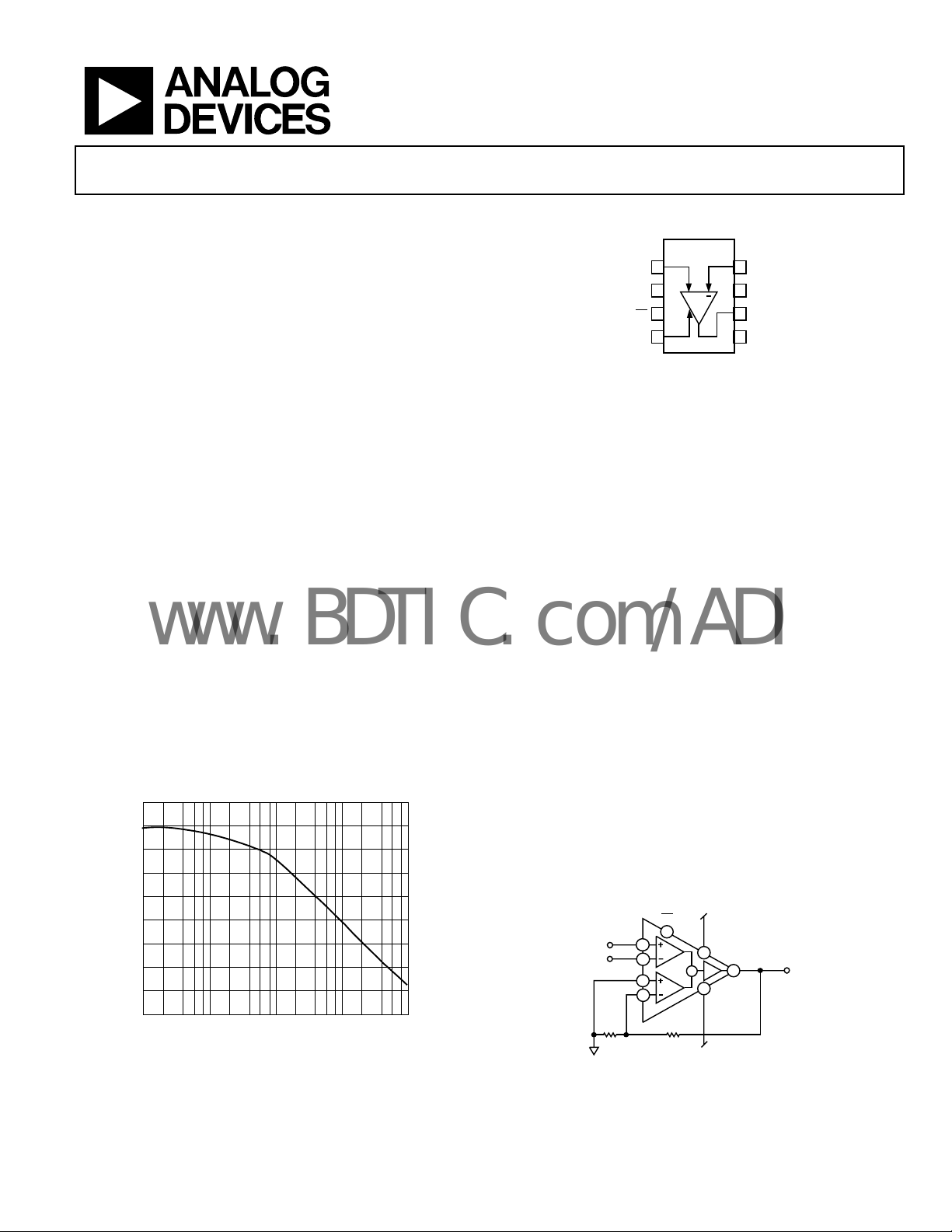
Figure 1.
The AD8129/AD8130 are differential-to-single-ended amplifiers
with extremely high CMRR at high frequency. Therefore, they
can also be effectively used as high speed instrumentation amps
or for converting differential signals to single-ended signals.
The AD8129 is a low noise, high gain (10 or greater) version
in
tended for applications over very long cables, where signal
attenuation is significant. The AD8130 is stable at a gain of 1
and can be used for applications where lower gains are required.
Both have user-adjustable gain to help compensate for losses in
the transmission line. The gain is set by the ratio of two resistor
values. The AD8129/AD8130 have very high input impedance
on both inputs, regardless of the gain setting.
8
–IN
+V
7
S
OUT
6
FB
5
02464-001
GENERAL DESCRIPTION
The AD8129/AD8130 are designed as receivers for the
transmission of high speed signals over twisted-pair cables to
work with the AD8131 or AD8132 drivers. Either can be used
f
or analog or digital video signals and for high speed data
transmission.
120
110
100
90
80
70
CMRR (dB)
60
50
40
30
10k 100k 1M 10M 100M
Figure 2. AD8129 CMRR vs. Frequency
Rev. C
Information furnished by Analog Devices is believed to be accurate and reliable. However, no
responsibility is assumed by Anal og Devices for its use, nor for any infringements of patents or ot her
rights of third parties that may result from its use. Specifications subject to change without notice. No
license is granted by implication or otherwise under any patent or patent rights of Analog Devices.
Trademarks and registered trademarks are the property of their respective owners.
FREQUENCY (Hz)
02464-002
The AD8129/AD8130 have excellent common-mode rejection
(70 dB @ 10 MHz), allowing the use of low cost, unshielded
twisted-pair cables without fear of corruption by external noise
sources or crosstalk. The AD8129/AD8130 have a wide power
supply range from single +5 V to ±12 V, allowing wide commonmode and differential-mode voltage ranges while maintaining
signal integrity. The wide common-mode voltage range enables
the driver-receiver pair to operate without isolation transformers
in many systems where the ground potential difference between
drive and receive locations is many volts. The AD8129/AD8130
have considerable cost and performance improvements over
op amps and other multiamplifier receiving solutions.
+V
S
PD
3
IN
R
G
V
OUT=VIN
1
8
4
5
[1+(RF/RG)]
7
6
2
R
F
–V
S
V
Figure 3. Typical Connection Configuration
OUT
02464-003
V
One Technology Way, P.O. Box 9106, Norwood, MA 02062-9106, U.S.A.
Tel: 781.329.4700 www.analog.com
Fax: 781.461.3113 © 2005 Analog Devices, Inc. All rights reserved.

AD8129/AD8130
www.BDTIC.com/ADI
TABLE OF CONTENTS
Features.............................................................................................. 1
Theory of Operation ...................................................................... 32
Applications....................................................................................... 1
Connection Diagram ....................................................................... 1
General Description ......................................................................... 1
Revision History ............................................................................... 2
AD8129/AD8130 Specifications..................................................... 3
5 V Specifications ......................................................................... 3
±5 V Specifications....................................................................... 5
±12 V Specifications..................................................................... 7
Absolute Maximum Ratings............................................................ 9
Thermal Resistance ...................................................................... 9
ESD Caution.................................................................................. 9
Typical Performance Characteristics ........................................... 10
AD8130 Frequency Response Characteristics........................ 10
AD8129 Frequency Response Characteristics........................ 13
AD8130 Harmonic Distortion Characteristics ......................16
AD8129 Harmonic Distortion Characteristics ......................18
Op Amp Configuration............................................................. 32
Applications..................................................................................... 33
Basic Gain Circuits..................................................................... 33
Twisted-Pair Cable, Composite Video Receiver with
Equalization Using an AD8130................................................... 33
Output Offset/Level Translator ................................................ 34
Resistorless Gain of 2................................................................. 35
Summer ....................................................................................... 35
Cable-Tap Amplifier .................................................................. 35
Power-Down ............................................................................... 36
Extreme Operating Conditions................................................ 36
Power Dissipation....................................................................... 37
Layout, Grounding, and Bypassing.......................................... 38
Outline Dimensions....................................................................... 39
Ordering Guide .......................................................................... 40
AD8130 Transient Response Characteristics.......................... 23
AD8129 Transient Response Characteristics.......................... 26
REVISION HISTORY
11/05—Rev. B to Rev. C
Changes to 5 V Specifications......................................................... 3
Changes to Table 4 and Maximum Power Dissipation Section.. 9
Changes to Figure 16...................................................................... 11
Changes to Figure 17...................................................................... 12
9/05—Rev. A to Rev. B
xtended Temperature Range...........................................Universal
E
Deleted Figure 5................................................................................ 5
Added Thermal Resistance Section ............................................... 9
Updated Outline Dimensions....................................................... 39
Changes to Ordering Guide.......................................................... 40
3/05—Rev. 0 to Rev. A
hanges to Specifications.................................................................2
C
Replaced Figure 3 ..............................................................................5
Changes to Ordering Guide.............................................................6
Updated Outline Dimensions....................................................... 27
Revision 0: Initial Version
Rev. C | Page 2 of 40

AD8129/AD8130
www.BDTIC.com/ADI
AD8129/AD8130 SPECIFICATIONS
5 V SPECIFICATIONS
AD8129 G = +10, AD8130 G = +1, TA = 25°C, +VS = 5 V, −VS = 0 V, REF = 2.5 V, PD ≥ VIH, RL = 1 kΩ, CL = 2 pF, unless otherwise noted.
to T
T
MIN
Table 1.
Model AD8129 AD8130
Parameter Conditions Min Typ Max Min Typ Max Unit
DYNAMIC PERFORMANCE
−3 dB Bandwidth V
V
Bandwidth for 0.1 dB
Slew Rate
Settling Time V
Rise and Fall Times
Output Overdrive Recovery 20 30 ns
NOISE/DISTORTION
Second Harmonic/Third
V
V
V
IMD V
Output IP3 V
Input Voltage Noise (RTI) f ≥ 10 kHz 4.5 12.3 nV/√Hz
Input Current Noise (+IN, −IN) f ≥ 100 kHz 1 1 pA/√Hz
Input Current Noise
Differential Gain Error
Differential Phase Error
INPUT CHARACTERISTICS
Common-Mode Rejection
V
V
CMRR with V
Common-Mode Voltage
Differential Operating Range ±0.5 ±2.5 V
Differential Clipping Level ±0.6 ±0.75 ±0.85 ±2.3 ±2.8 ±3.3 V
Resistance Differential 1 6 MΩ
Common mode 4 4 MΩ
Capacitance Differential 3 3 pF
Common mode 4 4 pF
= −40°C to +125°C, unless otherwise noted.
MAX
≤ 0.3 V p-p 160 185 220 250 MHz
OUT
= 1 V p-p 160 185 180 205 MHz
OUT
V
≤ 0.3 V p-p,
Flatness
OUT
SOIC/MSOP
= 2 V p-p, 25%
V
OUT
to 75%
= 2 V p-p, 0.1% 20 20 ns
OUT
≤ 1 V p-p, 10%
V
OUT
to 90%
V
= 1 V p-p, 5 MHz −68/−75 −72/−79 dBc
OUT
Harmonic
= 2 V p-p, 5 MHz −62/−64 −65/−71 dBc
OUT
= 1 V p-p, 10 MHz −63/−70 −60/−62 dBc
OUT
= 2 V p-p, 10 MHz −56/−58 −68/−68 dBc
OUT
= 2 V p-p, 10 MHz −67 −70 dBc
OUT
= 2 V p-p, 10 MHz 25 26 dBm
OUT
f ≥ 100 kHz 1.4 1.4 pA/√Hz
(REF, FB)
AD8130, G = +2, NTSC
100 IRE
AD8130, G = +2, NTSC
100 IRE
DC to 100 kHz,
Ratio
= 1 V p-p
OUT
= 1.5 V to 3.5 V
V
CM
= 1 V p-p @ 1 MHz 80 80 dB
CM
= 1 V p-p @ 10 MHz 70 70 dB
CM
= 1 V p-p @ 1 kHz,
V
CM
= ±0.5 V dc
V
OUT
V
− V
+IN
Range
, R
≥ 150 Ω
L
≥ 150 Ω
, R
L
= 0 V
−IN
25/40 25 MHz
810 930 810 930 V/μs
1.8 1.5 ns
0.3 0.13 %
0.1 0.15 Degrees
86 96 86 96 dB
80 72 dB
1.25 to
3.7
1.25 to
3.8
V
Rev. C | Page 3 of 40

AD8129/AD8130
www.BDTIC.com/ADI
Model AD8129 AD8130
Parameter Conditions Min Typ Max Min Typ Max Unit
DC PERFORMANCE
Closed-Loop Gain Error V
T
Open-Loop Gain V
Gain Nonlinearity V
Input Offset Voltage 0.2 0.8 0.4 1.8 mV
T
T
Input Offset Voltage vs.
Supply
Input Bias Current
(+IN, −IN)
Input Bias Current
(REF, FB)
Input Offset Current (+IN, −IN, REF, FB) ±0.08 ±0.4 ±0.08 ±0.4 μA
T
OUTPUT PERFORMANCE
Voltage Swing R
Output Current 35 35 mA
Short-Circuit Current To common −60/+55 −60/+55 mA
T
Output Impedance
POWER SUPPLY
Operating Voltage Range Total supply voltage ±2.25 ±12.6 ±2.25 ±12.6 V
Quiescent Supply Current 9.9 10.6 9.9 10.6 mA
T
PD
PIN
VIH +VS − 1.5 +VS − 1.5 V
VIL +VS − 2.5 +VS − 2.5 V
IIH
IIL
Input Resistance
Enable Time 0.5 0.5 μs
OPERATING TEMPERATURE
RANGE
= ±1 V, RL ≥ 150 Ω ±0.25 ±1.25 ±0.1 ±0.6 %
OUT
to T
MIN
OUT
OUT
MIN
MIN
+VS = 5 V, −VS = −0.5 V
20 20 ppm/°C
MAX
= ±1 V 86 71 dB
= ±1 V 250 200 ppm
to T
2 20 μV/°C
MAX
to T
1.4 3.5 mV
MAX
−88 −80 −74 −70 dB
to +0.5 V
= 0 V, +VS = +4.5 V
−V
S
−100 −86 −90 −76 dB
to +5.5 V
±0.5 ±2 ±0.5 ±2 μA
±1 ±3.5 ±1 ±3.5 μA
to T
T
MIN
(+IN, −IN,
MAX
5 5 nA/°C
REF, FB)
to T
MIN
LOAD
MIN
PD
≤ VIL, in power-
0.2 0.2 nA/°C
MAX
≥ 150 Ω 1.1 3.9 1.1 3.9 V
to T
−240 −240 μA/°C
MAX
10 10 pF
down mode
to T
MIN
PD
PD
≤ VIL
≤ VIL, T
33 33 μA/°C
MAX
0.65 0.85 0.65 0.85 mA
MIN
to T
MAX
1 1 mA
PD
= min VIH
PD
= max VIL
PD
≤ +VS − 3 V
PD
≥ +VS − 2 V
−30 −30 μA
−50 −50 μA
12.5 12.5 kΩ
100 100 kΩ
−40 +125 −40 +125 °C
Rev. C | Page 4 of 40

AD8129/AD8130
www.BDTIC.com/ADI
±5 V SPECIFICATIONS
AD8129 G = +10, AD8130 G = +1, TA = 25°C, VS = ±5 V, REF = 0 V, PD ≥ VIH, RL = 1 kΩ, CL = 2 pF, unless otherwise noted. T
= −40°C to +125°C, unless otherwise noted.
Table 2.
AD8129 AD8130
Parameter Conditions Min Typ Max Min Typ Max Unit
DYNAMIC PERFORMANCE
−3 dB Bandwidth V
V
Bandwidth for 0.1 dB
Flatness
Slew Rate
≤ 0.3 V p-p 175 200 240 270 MHz
OUT
= 2 V p-p 170 190 140 155 MHz
OUT
V
≤ 0.3 V p-p,
OUT
30/50 45 MHz
SOIC/MSOP
= 2 V p-p,
V
OUT
925 1060 950 1090 V/μs
25% to 75%
Settling Time V
Rise and Fall Times
= 2 V p-p, 0.1% 20 20 ns
OUT
≤ 1 V p-p,
V
OUT
1.7 1.4 ns
10% to 90%
Output Overdrive Recovery 30 40 ns
NOISE/DISTORTION
V
Second Harmonic/Third
= 1 V p-p, 5 MHz −74/−84 −79/−86 dBc
OUT
Harmonic
V
V
V
IMD V
Output IP3 V
= 2 V p-p, 5 MHz −68/−74 −74/−81 dBc
OUT
= 1 V p-p, 10 MHz −67/−81 −74/−80 dBc
OUT
= 1 V p-p, 10 MHz −61/−70 −74/−76 dBc
OUT
= 2 V p-p, 10 MHz −67 −70 dBc
OUT
= 2 V p-p, 10 MHz 25 26 dBm
OUT
Input Voltage Noise (RTI) f ≥ 10 kHz 4.5 12.5 nV/√Hz
Input Current Noise
f ≥ 100 kHz 1 1 pA/√Hz
(+IN, −IN)
Input Current Noise
f ≥ 100 kHz 1.4 1.4 pA/√Hz
(REF, FB)
Differential Gain Error
Differential Phase Error
AD8130, G = +2, NTSC
200 IR
L
≥ 150 Ω
E, R
AD8130, G = +2, NTSC
≥ 150 Ω
IRE, R
200
L
0.3 0.13 %
0.1 0.15 Degrees
INPUT CHARACTERISTICS
Common-Mode Rejection
Ratio
V
V
CMRR with V
= 1 V p-p
OUT
Common-Mode Voltage
DC to 100 kHz,
= −3 V to +3.5 V
V
CM
= 1 V p-p @ 2 MHz 80 80 dB
CM
= 1 V p-p @ 10 MHz 70 70 dB
CM
= 2 V p-p @ 1 kHz,
V
CM
= ±0.5 V dc
V
OUT
V
− V
+IN
= 0 V ±3.5 ±3.8 V
−IN
94 110 90 110 dB
100 83 dB
Range
Differential Operating
±0.5 ±2.5 V
Range
Differential Clipping Level ±0.6 ±0.75 ±0.85 ±2.3 ±2.8 ±3.3 V
Resistance Differential 1 6 MΩ
Common mode 4 4 MΩ
Capacitance Differential 3 3 pF
Common mode 4 4 pF
MIN
to T
MAX
Rev. C | Page 5 of 40

AD8129/AD8130
www.BDTIC.com/ADI
AD8129 AD8130
Parameter Conditions Min Typ Max Min Typ Max Unit
DC PERFORMANCE
Closed-Loop Gain Error V
T
Open-Loop Gain V
Gain Nonlinearity V
Input Offset Voltage 0.2 0.8 0.4 1.8 mV
T
T
Input Offset Voltage vs.
Supply
Input Bias Current
(+IN, −IN)
Input Bias Current (REF, FB) ±1 ±3.5 ±1 ±3.5 μA
Input Offset Current (+IN, −IN, REF, FB) ±0.08 ±0.4 ±0.08 ±0.4 μA
T
OUTPUT PERFORMANCE
Voltage Swing R
Output Current 40 40
Short-Circuit Current To common −60/+55 −60/+55
T
Output Impedance
POWER SUPPLY
Operating Voltage Range Total supply voltage ±2.25 ±12.6 ±2.25 ±12.6 V
Quiescent Supply Current 10.8 11.6 10.8 11.6 mA
T
PD
PIN
VIH +VS − 1.5 +VS − 1.5 V
VIL +VS − 2.5 +VS − 2.5 V
IIH
IIL
Input Resistance
Enable Time 0.5 0.5 μs
OPERATING TEMPERATURE
RANGE
= ±1 V, RL ≥ 150 Ω ±0.4 ±1.5 ±0.15 ±0.6 %
OUT
to T
MIN
OUT
OUT
MIN
MIN
+VS = +5 V, −VS = −4.5 V
20 10 ppm/°C
MAX
= ±1 V 88 74 dB
= ±1 V 250 200 ppm
to T
2 20 μV/°C
MAX
to T
1.4 3.5 mV
MAX
−90 −84 −78 −74 dB
to −5.5 V
= −5 V, +VS = +4.5 V
−V
S
−94 −86 −80 −74 dB
to +5.5 V
±0.5 ±2 ±0.5 ±2 μA
to T
T
MIN
(+IN, −IN,
MAX
5 5 nA/°C
REF, FB)
to T
MIN
LOAD
MIN
PD
≤ VIL, in power-
0.2 0.2 nA/°C
MAX
= 150 Ω/1 kΩ 3.6/4.0 3.6/4.0 ±V
to T
−240 −240 μA/°C
MAX
10 10
mA
mA
pF
down mode
to T
MIN
PD
PD
≤ VIL
≤ VIL, T
36 36 μA/°C
MAX
0.68 0.85 0.68 0.85 mA
MIN
to T
MAX
1 1 mA
PD
= min VIH
PD
= max VIL
PD
≤ +VS − 3 V
PD
≥ +VS − 2 V
−30 −30 μA
−50 −50 μA
12.5 12.5 kΩ
100 100 kΩ
−40 +125 −40 +125 °C
Rev. C | Page 6 of 40

AD8129/AD8130
www.BDTIC.com/ADI
±12 V SPECIFICATIONS
AD8129 G = +10, AD8130 G = +1, TA = 25°C, VS = ±12 V, REF = 0 V, PD ≥ VIH, RL = 1 kΩ, CL = 2 pF, unless otherwise noted. T
= −40°C to +85°C, unless otherwise noted.
T
MAX
Table 3.
AD8129 AD8130
Parameter Conditions Min Typ Max Min Typ Max Unit
DYNAMIC PERFORMANCE
−3 dB Bandwidth V
V
Bandwidth for 0.1 dB Flatness
≤ 0.3 V p-p 175 200 250 290 MHz
OUT
= 2 V p-p 170 195 150 175 MHz
OUT
≤ 0.3 V p-p,
V
OUT
50/70 110 MHz
SOIC/MSOP
Slew Rate
= 2 V p-p, 25%
V
OUT
935 1070 960 1100 V/μs
to 75%
Settling Time V
Rise and Fall Times
= 2 V p-p, 0.1% 20 20 ns
OUT
≤ 1 V p-p, 10%
V
OUT
1.7 1.4 ns
to 90%
Output Overdrive Recovery 40 40 ns
NOISE/DISTORTION
V
Second Harmonic/Third
= 1 V p-p, 5 MHz −71/−84 −79/−86 dBc
OUT
Harmonic
V
V
V
IMD V
Output IP3 V
= 2 V p-p, 5 MHz −65/−74 −74/−81 dBc
OUT
= 1 V p-p, 10 MHz −65/−82 −74/−80 dBc
OUT
= 2 V p-p, 10 MHz −59/−70 −74/−74 dBc
OUT
= 2 V p-p, 10 MHz −67 −70 dBc
OUT
= 2 V p-p, 10 MHz 25 26 dBm
OUT
Input Voltage Noise (RTI) f ≥ 10 kHz 4.6 13 nV/√Hz
Input Current Noise
f ≥ 100 kHz 1 1 pA/√Hz
(+IN, −IN)
Input Current Noise
f ≥ 100 kHz 1.4 1.4 pA/√Hz
(REF, FB)
Differential Gain Error
Differential Phase Error
AD8130, G = +2, NTSC
200 IRE
L
≥ 150 Ω
, R
AD8130, G = +2, NTSC
≥ 150 Ω
, R
200 IRE
L
0.3 0.13 %
0.1 0.2 Degrees
INPUT CHARACTERISTICS
Common-Mode Rejection
Ratio
V
V
CMRR with V
= 1 V p-p
OUT
Common-Mode Voltage
DC to 100 kHz,
= ±10 V
V
CM
= 1 V p-p @ 2 MHz 80 80 dB
CM
= 1 V p-p @ 10 MHz 70 70 dB
CM
= 4 V p-p @ 1 kHz,
V
CM
= ±0.5 V dc
V
OUT
V
− V
+IN
= 0 V ±10.3 ±10.5 V
–IN
92 105 88 105 dB
93 80 dB
Range
Differential Operating Range ±0.5 ±2.5 V
Differential Clipping Level ±0.6 ±0.75 ±0.85 ±2.3 ±2.8 ±3.3 V
Resistance Differential 1 6 MΩ
Common mode 4 4 MΩ
Capacitance Differential 3 3 pF
Common mode 4 4 pF
MIN
to
Rev. C | Page 7 of 40

AD8129/AD8130
www.BDTIC.com/ADI
AD8129 AD8130
Parameter Conditions Min Typ Max Min Typ Max Unit
DC PERFORMANCE
Closed-Loop Gain Error V
T
Open-Loop Gain V
Gain Nonlinearity V
Input Offset Voltage 0.2 0.8 0.4 1.8 mV
T
T
Input Offset Voltage vs. Supply
Input Bias Current (+IN, −IN) ±0.25 ±2 ±0.25 ±2 μA
Input Bias Current (REF, FB) ±0.5 ±3.5 ±0.5 ±3.5 μA
Input Offset Current (+IN, −IN, REF, FB) ±0.08 ±0.4 ±0.08 ±0.4 μA
T
OUTPUT PERFORMANCE
Voltage Swing R
Output Current 40 40
Short-Circuit Current To common −60/+55 −60/+55
T
Output Impedance
POWER SUPPLY
Operating Voltage Range Total supply voltage ±2.25 ±12.6 ±2.25 ±12.6 V
Quiescent Supply Current 13 13.9 13 13.9 mA
T
PD
PIN
V
+VS − 1.5 +VS − 1.5 V
IH
V
+VS − 2.5 +VS − 2.5 V
IL
IIH
IIL
Input Resistance
Enable Time 0.5 0.5 μs
OPERATING TEMPERATURE
RANGE
= ±1 V, RL ≥ 150 Ω ±0.8 ±1.8 ±0.15 ±0.6 %
OUT
to T
20 10 ppm/°C
MAX
= ±1 V 87 73 dB
= ±1 V 250 200 ppm
to T
2 20 μV/°C
MAX
to T
1.4 3.5 mV
MAX
= +12 V, −VS =
−88 −82 −77 −70 dB
+V
MIN
OUT
OUT
MIN
MIN
S
–11.0 V to −13.0 V
= −12 V, +VS =
−V
S
−92 −84 −88 −70 dB
+11.0 V to +13.0 V
to T
MAX
T
MIN
2.5 2.5 nA/°C
(+IN, −IN, REF, FB)
to T
MIN
LOAD
MIN
PD
0.2 0.2 nA/°C
MAX
= 700 Ω ±10.8 ±10.8
to T
−240 −240 μA/°C
MAX
≤ VIL, in power-
10 10
V
mA
mA
pF
down mode
to T
MIN
PD
PD
43 43 μA°C
MAX
≤ VIL
≤ VIL, T
MIN
to T
MAX
0.73 0.9 0.73 0.9 mA
1.1 1.1 mA
PD
= min VIH
PD
= max VIL
PD
≤ +VS − 3 V
PD
≥ +VS − 2 V
−30 −30 μA
−50 −50 μA
3 3 kΩ
100 100 kΩ
−40 +85 −40 +85 °C
Rev. C | Page 8 of 40
AD8129/AD8130
www.BDTIC.com/ADI
ABSOLUTE MAXIMUM RATINGS
Table 4.
Parameter Rating
Supply Voltage 26.4 V
Power Dissipation Refer to Figure 4
Input Voltage (Any Input) −VS − 0.3 V to +VS + 0.3 V
Differential Input Voltage (AD8129)
VS ≥ ±11.5 V ±0.5 V
Differential Input Voltage (AD8129)
VS < ±11.5 V ±6.2 V
Differential Input Voltage (AD8130) ±8.4 V
Storage Temperature Range −65°C to +150°C
Lead Temperature (Soldering, 10 sec) 300°C
Junction Temperature 150°C
Stresses above those listed under Absolute Maximum Ratings
may cause permanent damage to the device. This is a stress
rating only; functional operation of the device at these or any
other conditions above those indicated in the operational
section of this specification is not implied. Exposure to absolute
maximum rating conditions for extended periods may affect
device reliability.
THERMAL RESISTANCE
θJA is specified for the worst-case conditions, that is, θJA is
specified for the device soldered in a circuit board in still air.
Table 5. Thermal Resistance
Package Type θJA Unit
8-Lead SOIC/4-Layer 121 °C/W
8-Lead MSOP/4-Layer 142 °C/W
Maximum Power Dissipation
The maximum safe power dissipation in the AD8129/AD8130
packages is limited by the associated rise in junction temperature (T
glass transition temperature, the plastic changes its properties.
Even temporarily exceeding this temperature limit can change
the stresses that the package exerts on the die, permanently
shifting the parametric performance of the AD8129/AD8130.
Exceeding a junction temperature of 150°C for an extended
period can result in changes in the silicon devices, potentially
causing failure.
) on the die. At approximately 150°C, which is the
J
The power dissipated in the package (P
quiescent power dissipation and the power dissipated in the
package due to the load drive. The quiescent power is the
voltage between the supply pins (V
current (I
). The power dissipated due to the load drive
S
depends upon the particular application. The power due to
load drive is calculated by multiplying the load current by the
associated voltage drop across the device. RMS voltages and
currents must be used in these calculations.
Airflow reduces θ
. In addition, more metal directly in contact
JA
with the package leads from metal traces through holes, ground,
and power planes reduces the θ
JA
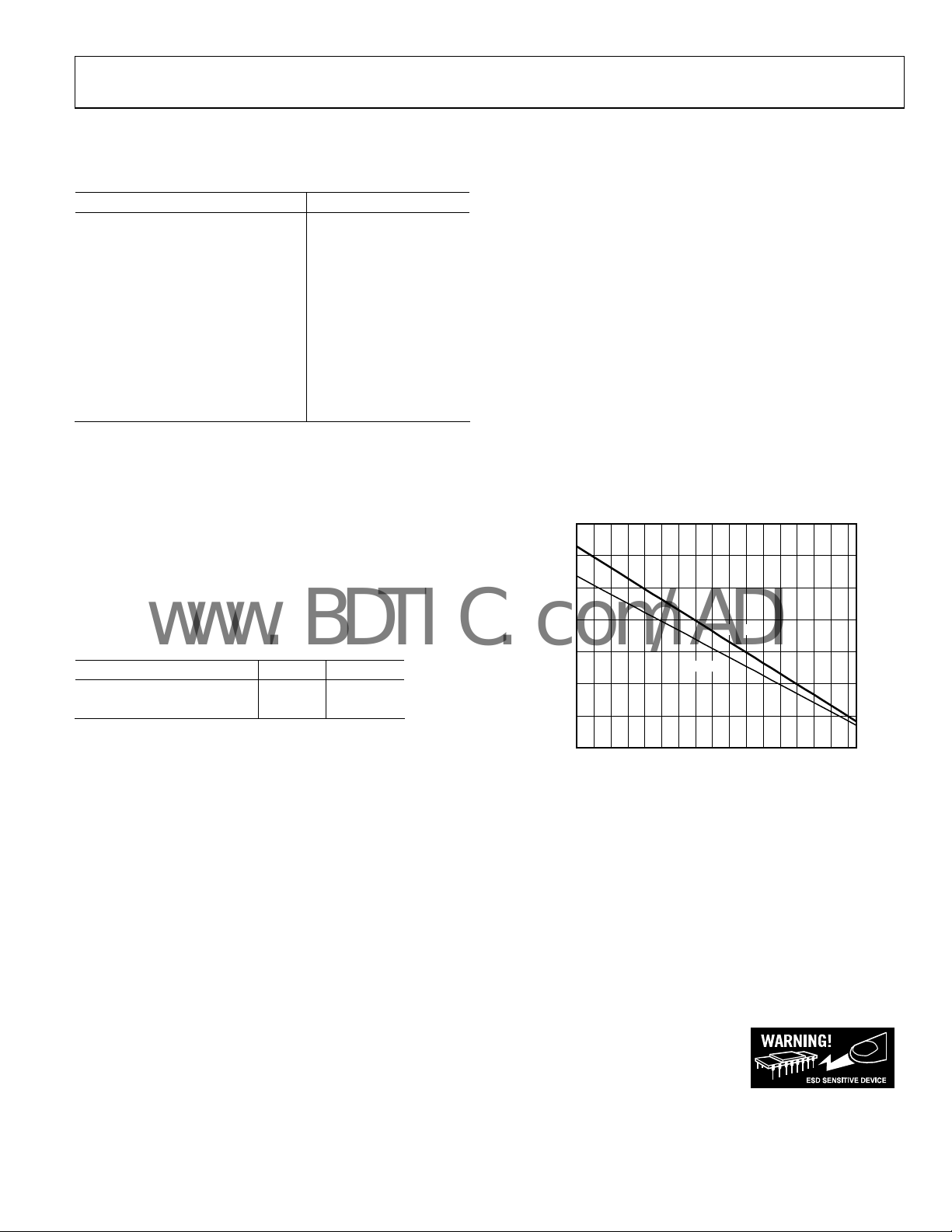
Figure 4 shows the maximum safe power dissipation in the
ackage vs. the ambient temperature for the 8-lead SOIC
p
(121°C/W) and MSOP (θ
standard 4-layer board. θ
1.75
1.50
1.25
1.00
0.75
0.50
MAXIMUM POWER DISSIPATION (W)
0.25
0
–40–30 –20 –10 0 10 20 30 40 50 60 70 80 90 100 110120
Figure 4. Maximum Power Dissipation vs. Temperature
= 142°C/W) packages on a JEDEC
JA
values are approximations.
JA
MSOP
AMBIENT TEMPERATURE (°C)
) is the sum of the
D
) times the quiescent
S
.
SOIC
02464-005
ESD CAUTION
ESD (electrostatic discharge) sensitive device. Electrostatic charges as high as 4000 V readily accumulate on
the human body and test equipment and can discharge without detection. Although this product features
proprietary ESD protection circuitry, permanent damage may occur on devices subjected to high energy
electrostatic discharges. Therefore, proper ESD precautions are recommended to avoid performance
degradation or loss of functionality.
Rev. C | Page 9 of 40
AD8129/AD8130
www.BDTIC.com/ADI
TYPICAL PERFORMANCE CHARACTERISTICS
AD8130 FREQUENCY RESPONSE CHARACTERISTICS
G = +1, RL = 1 kΩ, CL = 2 pF, V
3
V
= 0.3V p-p
OUT
2
1
0
–1
–2
GAIN (dB)
–3
–4
–5
–6
–7
1 10 100 400
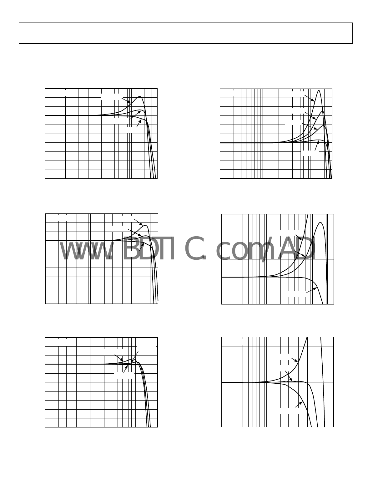
Figure 5. AD8130 Frequency Response vs. Supply, V
3
V
= 1V p-p
OUT
2
1
0
–1
–2
GAIN (dB)
–3
–4
–5
–6
–7
1
Figure 6. AD8130 Frequency Response vs. Supply, V
3
V
= 2V p-p
OUT
2
1
0
–1
–2
GAIN (dB)
–3
–4
–5
–6
–7
1
Figure 7. AD8130 Frequency Response vs. Supply, V
FREQUENCY (MHz)
FREQUENCY (MHz)
FREQUENCY (MHz)
= 0.3 V p-p, TA = 25°C, unless otherwise noted.
OUT
VS = ±2.5V
VS = ±5V
VS = ±12V
02464-006
= 0.3 V p-p
OUT
VS = ±2.5V
VS = ±5V
VS = ±12V
10 100 300
02464-007
= 1 V p-p
OUT
VS = ±2.5V
VS = ±12V
10 100 300
VS = ±5V
02464-008
= 2 V p-p
OUT
6
VS =±5V
5
4
3
2
1
GAIN (dB)
0
–1
–2
–3
–4
1
10 100 300
FREQUENCY (MHz)
CL = 20pF
CL = 10pF
CL = 5pF
CL = 2pF
Figure 8. AD8130 Frequency Response vs. Load Capacitance
0.7
RL = 1kΩ
0.6
0.5
0.4
0.3
0.2
GAIN (dB)
0.1
0
–0.1
–0.2
–0.3
1
FREQUENCY (MHz)
Figure 9. AD8130 Fine Scale Response vs. Supply, R
VS = ±2.5V
VS = ±5V
VS = ±12V
10 100 300
= 1 kΩ
L
0.5
RL = 150Ω
0.4
0.3
0.2
0.1
0
GAIN (dB)
–0.1
–0.2
–0.3
–0.4
–0.5
1
Figure 10. AD8130 Fine Scale Response vs. Supply, R
VS = ±2.5V
VS = ±5V
VS = ±12V
10 100 300
FREQUENCY (MHz)
= 150 Ω
L
02464-009
02464-010
02464-011
Rev. C | Page 10 of 40
AD8129/AD8130
www.BDTIC.com/ADI
3
RL = 150Ω
2
1
0
–1
–2
GAIN (dB)
–3
–4
–5
–6
–7
1
FREQUENCY (MHz)
VS = ±2.5V
VS = ±5V
VS = ±12V
10 100 400
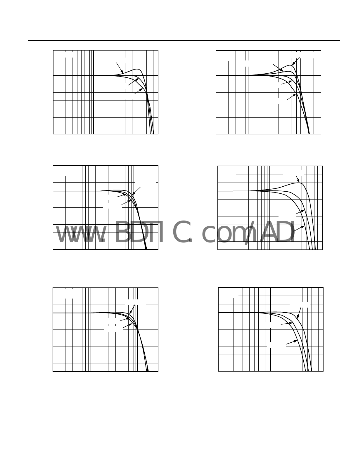
Figure 11. AD8130 Frequency Response vs. Supply, R
3
G = +2
V
= 0.3V p-p
OUT
2
1
0
–1
–2
GAIN (dB)
–3
–4
–5
–6
–7
1
VS = ±5V
VS = ±12V
10 100 300
FREQUENCY (MHz)
Figure 12. AD8130 Frequency Response vs. Supply,
G = +2,
= 0.3 V p-p
V
OUT
3
G = +2
V
= 2V p-p
2
OUT
1
0
–1
–2
GAIN (dB)
–3
–4
–5
–6
–7
1
VS = ±5V
VS = ±12V
10 100 300
FREQUENCY (MHz)
VS = ±2.5V
Figure 13. AD8130 Frequency Response vs. Supply,
= 2 V p-p
+2, V
G =
OUT
= 150 Ω
L
VS = ±2.5V
02464-012
02464-013
02464-014
3
G = +2
= ±5V
V
S
2
1
0
–1
–2
GAIN (dB)
–3
–4
–5
–6
–7
1
RF = RG = 750Ω
RF = RG = 499Ω
RF = RG = 250Ω
10 100 300
FREQUENCY (MHz)
RF = RG = 1kΩ
Figure 14. AD8130 Frequency Response for Various R
0.3
G = +2
R
= 1kΩ
L
0.2
0.1
0
–0.1
–0.2
GAIN (dB)
–0.3
–0.4
–0.5
–0.6
–0.7
1 10 100
FREQUENCY (MHz)
VS = ±2.5V
VS = ±5V
VS = ±12V
Figure 15. AD8130 Fine Scale Response vs. Supply,
= 1 kΩ
+2, R
G =
L
0.3
G=+2
= 150
Ω
R
L
0.2
0.1
0
–0.1
–0.2
GAIN (dB)
–0.3
–0.4
–0.5
–0.6
–0.7
110
VS=±5V
VS=±12V
FREQUENCY (MHz)
VS=±2.5V
Figure 16. AD8130 Fine Scale Response vs. Supply,
G =
+2, R
= 150 Ω
L
02464-015
F/RG
02464-016
02464-017
100
Rev. C | Page 11 of 40
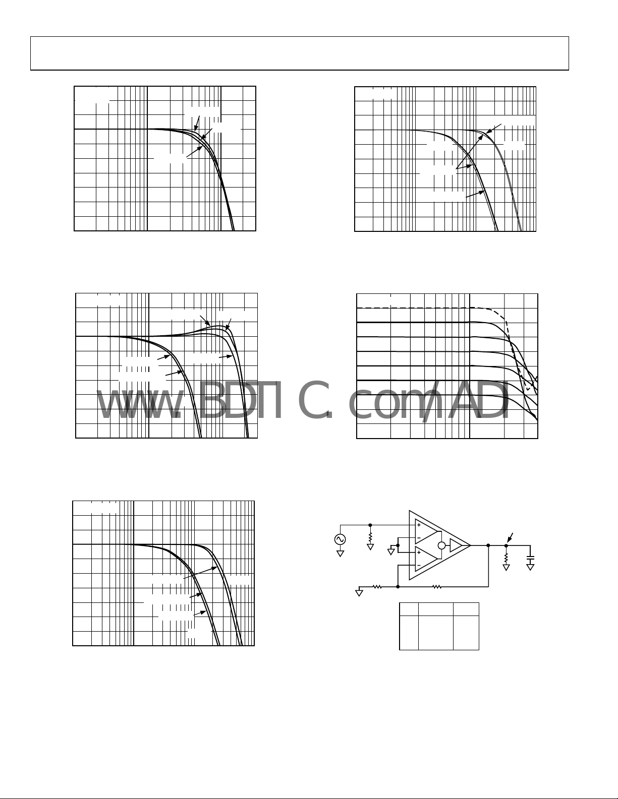
AD8129/AD8130
www.BDTIC.com/ADI
3
G=+2
R
= 150Ω
L
2
1
0
–1
–2
GAIN (dB)
–3
–4
–5
–6
–7
1 30010 100
VS=±12V
FREQUENCY (MHz)
Figure 17. AD8130 Frequency Response vs. Supply,
G =
+2, R
= 150 Ω
L
0.3
V
= 2V p-p
OUT
0.2
0.1
0
–0.1
–0.2
GAIN (dB)
–0.3
–0.4
–0.5
–0.6
–0.7
0.1
VS = ±2.5V
VS = ±5V, ±12V
FREQUENCY (MHz)
VS = ±2.5V
G = +10 G = +5
110
Figure 18. AD8130 Fine Scale Response vs. Supply,
+5, G = +10, V
G =
= 2 V p-p
OUT
VS= ±2.5V
VS = ±12V
VS=±5V
VS = ±5V
02464-018
02464-019
30
3
RL = 150
2
1
0
–1
–2
GAIN (dB)
–3
–4
–5
–6
–7
0.1
Ω
VS = ±5V, ±12V
G = +10 G = +5
VS = ±2.5V
VS = ±5V, ±12V
1 10 100
FREQUENCY (MHz)
Figure 20. AD8130 Frequency Response vs. Supply,
+5, G = +10, R
G =
= 150 Ω
L
12
0dB = 1V rms
6
0
–6
–12
–18
–24
–30
OUTPUT VOLTAGE (dBV)
–36
–42
VS =±5V
–48
10
FREQUENCY (MHz)
100 400
Figure 21. AD8130 Frequency Response for Various Output Levels
02464-021
02464-022
3
V
= 2V p-p
OUT
2
1
0
–1
–2
GAIN (dB)
–3
–4
–5
–6
–7
0.1
VS = ±12V
VS = ±5V, ±12V
VS = ±2.5V
G = +10
1 10 100
FREQUENCY (MHz)
Figure 19. AD8130 Frequency Response vs. Supply,
G = +5, G = +10, V
= 2 V p-p
OUT
G = +5
02464-020
1
50Ω
R
8
4
5
G
G
1
2
5
10
Figure 22. AD8130 Basic Frequency Respo
R
R
F
0Ω
499Ω
8.06kΩ
4.99kΩ
TEK P6245
FET PROBE
6
R
C
L
L
F
R
G
–
499Ω
2kΩ
549Ω
02464-023
nse Test Circuit
Rev. C | Page 12 of 40
 Loading...