

Quad 150 MHz
NORMALIZED GAIN – dB
1M 10M 100M
FREQUENCY – Hz
15
12
9
6
3
0
–3
–6
–9
VS = +5V
G = +1
–12
18
100k
a
FEATURES
Single AD8041 and Dual AD8042 Also Available
Fully Specified at +3 V, +5 V, and ⴞ5 V Supplies
Output Swings to Within 25 mV of Either Rail
Input Voltage Range Extends 200 mV Below Ground
No Phase Reversal with Inputs 1 V Beyond Supplies
Low Power of 2.75 mA/Amplifier
High Speed and Fast Settling on +5 V
150 MHz –3 dB Bandwidth (G = +1)
170 V/s Slew Rate
40 ns Settling Time to 0.1%
Good Video Specifications (R
Gain Flatness of 0.1 dB to 12 MHz
0.06% Differential Gain Error
0.15ⴗ Differential Phase Error
Low Distortion
–68 dBc Total Harmonic @ 5 MHz
Outstanding Load Drive Capability
Drives 30 mA 0.5 V from Supply Rails
APPLICATIONS
Active Filters
Video Switchers
Distribution Amplifiers
A/D Driver
Professional Cameras
CCD Imaging Systems
Ultrasound Equipment (Multichannel)
PRODUCT DESCRIPTION
The AD8044 is a quad low power, voltage feedback, high speed
amplifier designed to operate on +3 V, +5 V or ±5 V supplies.
It has true single-supply capability with an input voltage range
extending 200 mV below the negative rail and within 1 V of the
positive rail.
= 150 ⍀, G = +2)
L
Rail-to-Rail Amplifier
AD8044
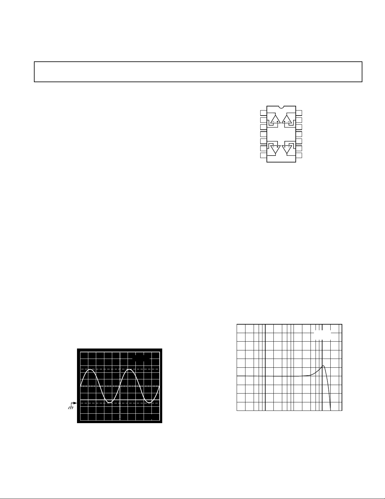
CONNECTION DIAGRAM
14-Lead Plastic DIP and SOIC
1
OUT A
2
–IN A
3
+IN A
4
V+
AD8044
5
+IN B
6
–IN B
7
OUT B
TOP VIEW
The output voltage swing extends to within 25 mV of each rail,
providing the maximum output dynamic range. Additionally, it
features gain flatness of 0.1 dB to 12 MHz while offering differ-
ential gain and phase error of 0.04% and 0.22° on a single +5 V
supply. This makes the AD8044 useful for video electronics
such as cameras, video switchers or any high speed portable
equipment. The AD8044’s low distortion and fast settling make
it ideal for active filter applications.
The AD8044 offers low power supply current of 13.1 mA max
and can run on a single +3.3 V power supply. These features are
ideally suited for portable and battery powered applications
where size and power are critical.
The wide bandwidth of 150 MHz along with 170 V/µs of slew
rate on a single +5 V supply make the AD8044 useful in many
general purpose, high speed applications where dual power
supplies of up to ±6 V and single supplies from +3 V to +12 V
are needed. The AD8044 is available in 14-lead plastic DIP and
SOIC.
14
OUT D
13
–IN D
+IN D
12
V–
11
10
+IN C
9
–IN C
8
OUT C
REV. A
Information furnished by Analog Devices is believed to be accurate and
reliable. However, no responsibility is assumed by Analog Devices for its
use, nor for any infringements of patents or other rights of third parties
which may result from its use. No license is granted by implication or
otherwise under any patent or patent rights of Analog Devices.
VS = +5V
5V
2.5V
0V
1V
2ms
Figure 1. Output Swing: Gain = –1, RL = 2 k
Ω
Figure 2. Frequency Response: Gain = +1, VS = +5 V
One Technology Way, P.O. Box 9106, Norwood, MA 02062-9106, U.S.A.
Tel: 781/329-4700 World Wide Web Site: http://www.analog.com
Fax: 781/326-8703 © Analog Devices, Inc., 1999

AD8044–SPECIFICATIONS
(@ TA = +25ⴗC, VS = +5 V, RL = 2 k⍀ to 2.5 V, unless otherwise noted)
AD8044A
Parameter Conditions Min Typ Max Units
DYNAMIC PERFORMANCE
–3 dB Small Signal Bandwidth, V
Bandwidth for 0.1 dB Flatness G = +2, R
Slew Rate G = –1, V
Full Power Response V
Settling Time to 1% G = –1, V
< 0.5 V p-p G = +1 80 150 MHz
O
= 2 V p-p 26 MHz
O
= 150 Ω 12 MHz
L
= 4 V Step 140 170 V/µs
O
= 2 V Step 30 ns
O
Settling Time to 0.1% 40 ns
NOISE/DISTORTION PERFORMANCE
Total Harmonic Distortion f
= 5 MHz, VO = 2 V p-p, G = +2, R
C
= 1 kΩ –68 dB
L
Input Voltage Noise f = 10 kHz 16 nV/√Hz
Input Current Noise f = 10 kHz 850 fA/√Hz
Differential Gain Error (NTSC) G = +2, R
Differential Phase Error (NTSC) G = +2, R
Crosstalk f = 5 MHz, R
= 150 Ω to 2.5 V 0.04 %
L
= 150 Ω to 2.5 V 0.22 Degrees
L
= 1 kΩ, G = +2 –60 dB
L
DC PERFORMANCE
Input Offset Voltage 1.0 6 mV
T
MIN–TMAX
8mV
Offset Drift 8 µV/°C
Input Bias Current 2 4.5 µA
T
MIN–TMAX
4.5 µA
Input Offset Current 0.2 1.2 µA
Open-Loop Gain R
= 1 kΩ 82 94 dB
L
T
MIN–TMAX
88 dB
INPUT CHARACTERISTICS
Input Resistance 225 kΩ
Input Capacitance 1.6 pF
Input Common-Mode Voltage Range –0.2 to 4 V
Common-Mode Rejection Ratio VCM = 0 V to 3.5 V 80 90 dB
OUTPUT CHARACTERISTICS
Output Voltage Swing R
Output Voltage Swing: R
Output Voltage Swing: R
Output Current T
= 10 kΩ to 2.5 V 0.03 to 4.975 V
L
= 1 kΩ to 2.5 V 0.25 to 4.75 0.075 to 4.91 V
L
= 150 Ω to 2.5 V 0.55 to 4.4 0.25 to 4.65 V
L
MIN–TMAX, VOUT
= 0.5 V to 4.5 V 30 mA
Short Circuit Current Sourcing 45 mA
Sinking 85 mA
Capacitive Load Drive G = +2 40 pF
POWER SUPPLY
Operating Range 312V
Quiescent Current 11 13.1 mA
Power Supply Rejection Ratio V
= 0, +5 V, ±1 V 70 80 dB
S
OPERATING TEMPERATURE RANGE –40 +85 °C
Specifications subject to change without notice.
–2–
REV. A

SPECIFICATIONS
(@ TA = +25ⴗC, VS = +3 V, RL = 2 k⍀ to 1.5 V, unless otherwise noted)
AD8044
AD8044A
Parameter Conditions Min Typ Max Units
DYNAMIC PERFORMANCE
–3 dB Small Signal Bandwidth, V
Bandwidth for 0.1 dB Flatness G = +2, R
Slew Rate G = –1, V
Full Power Response V
Settling Time to 1% G = –1, V
< 0.5 V p-p G = +1 80 135 MHz
O
O
= 150 Ω 10 MHz
L
= 2 V Step 110 150 V/µs
O
= 2 V p-p 22 MHz
= 2 V Step 35 ns
O
Settling Time to 0.1% 55 ns
NOISE/DISTORTION PERFORMANCE
Total Harmonic Distortion f
= 5 MHz, VO = 2 V p-p, G = –1, R
C
= 100 Ω –48 dB
L
Input Voltage Noise f = 10 kHz 16 nV/√Hz
Input Current Noise f = 10 kHz 600 fA/√Hz
Differential Gain Error (NTSC) G = +2, R
Differential Phase Error (NTSC) G = +2, R
Crosstalk f = 5 MHz, R
= 150 Ω to 1.5 V, Input V
L
= 150 Ω to 1.5 V, Input V
L
= 1 kΩ, G = +2 –60 dB
L
= 0.5 V 0.13 %
CM
= 0.5 V 0.3 Degrees
CM
DC PERFORMANCE
Input Offset Voltage 1.5 5.5 mV
T
MIN–TMAX
7.5 mV
Offset Drift 8 µV/°C
Input Bias Current 2 4.5 µA
T
MIN–TMAX
4.5 µA
Input Offset Current 0.2 1.2 µA
Open-Loop Gain R
= 1 kΩ 80 92 dB
L
T
MIN–TMAX
88 dB
INPUT CHARACTERISTICS
Input Resistance 225 kΩ
Input Capacitance 1.6 pF
Input Common-Mode Voltage Range –0.2 to 2 V
Common-Mode Rejection Ratio VCM = 0 V to 1.5 V 76 90 dB
OUTPUT CHARACTERISTICS
Output Voltage Swing R
Output Voltage Swing: R
Output Voltage Swing: R
Output Current T
= 10 kΩ to 1.5 V 0.025 to 2.98 V
L
= 1 kΩ to 1.5 V 0.17 to 2.82 0.06 to 2.93 V
L
= 150 Ω to 1.5 V 0.35 to 2.55 0.15 to 2.75 V
L
MIN–TMAX, VOUT
= 0.5 V to 2.5 V 25 mA
Short Circuit Current Sourcing 30 mA
Sinking 50 mA
Capacitive Load Drive G = +2 35 pF
POWER SUPPLY
Operating Range 312V
Quiescent Current 10.5 12.5 mA
Power Supply Rejection Ratio VS = 0, +3 V, +0.5 V 70 80 dB
OPERATING TEMPERATURE RANGE 0 +70 °C
Specifications subject to change without notice.
REV. A –3–

AD8044–SPECIFICATIONS
(@ TA = +25ⴗC, VS = ⴞ5 V, RL = 2 k⍀ to 0 V, unless otherwise noted)
AD8044A
Parameter Conditions Min Typ Max Units
DYNAMIC PERFORMANCE
–3 dB Small Signal Bandwidth, V
Bandwidth for 0.1 dB Flatness G = +2, R
Slew Rate G = –1, V
Full Power Response V
Settling Time to 0.1% G = –1, V
< 0.5 V p-p G = +1 85 160 MHz
O
= 2 V p-p 29 MHz
O
= 150 Ω 15 MHz
L
= 8 V Step 150 190 V/µs
O
= 2 V Step 30 ns
O
Settling Time to 0.01% 40 ns
NOISE/DISTORTION PERFORMANCE
Total Harmonic Distortion f
= 5 MHz, VO = 2 V p-p, G = +2 –72 dB
C
Input Voltage Noise f = 10 kHz 16 nV/√Hz
Input Current Noise f = 10 kHz 900 fA/√Hz
Differential Gain Error (NTSC) G = +2, R
Differential Phase Error (NTSC) G = +2, R
Crosstalk f = 5 MHz, R
= 150 Ω 0.06 %
L
= 150 Ω 0.15 Degrees
L
= 1 kΩ, G = +2 –60 dB
L
DC PERFORMANCE
Input Offset Voltage 1.4 6.5 mV
T
MIN–TMAX
9mV
Offset Drift 10 µV/°C
Input Bias Current 2 4.5 µA
T
MIN–TMAX
4.5 µA
Input Offset Current 0.2 1.2 µA
Open-Loop Gain R
= 1 kΩ 82 96 dB
L
T
MIN–TMAX
92 dB
INPUT CHARACTERISTICS
Input Resistance 225 kΩ
Input Capacitance 1.6 pF
Input Common-Mode Voltage Range –5.2 to 4 V
Common-Mode Rejection Ratio VCM = –5 V to 3.5 V 76 90 dB
OUTPUT CHARACTERISTICS
Output Voltage Swing R
Output Voltage Swing: R
Output Voltage Swing: R
Output Current T
= 10 kΩ –4.97 to +4.97 V
L
= 1 kΩ –4.6 to +4.6 –4.85 to +4.85 V
L
= 150 Ω –4.0 to +3.8 –4.5 to +4.5 V
L
MIN–TMAX, VOUT
= –4.5 V to +4.5 V 30 mA
Short Circuit Current Sourcing 60 mA
Sinking 100 mA
Capacitive Load Drive G = +2 40 pF
POWER SUPPLY
Operating Range 312V
Quiescent Current 11.5 13.6 mA
Power Supply Rejection Ratio V
= –5, +5 V, ±1 V 70 80 dB
S
OPERATING TEMPERATURE RANGE –40 +85 °C
Specifications subject to change without notice.
REV. A–4–
AD8044
WARNING!
ESD SENSITIVE DEVICE
ABSOLUTE MAXIMUM RATINGS
Supply Voltage . . . . . . . . . . . . . . . . . . . . . . . . . . . . . . . +12.6 V
Internal Power Dissipation
2
1
Plastic DIP Package (N) . . . . . . . . . . . . . . . . . . . 1.6 Watts
Small Outline Package (R) . . . . . . . . . . . . . . . . . . 1.0 Watts
Input Voltage (Common Mode) . . . . . . . . . . . . . . ±V
± 0.5 V
S
Differential Input Voltage . . . . . . . . . . . . . . . . . . . . . . . ±3.4 V
Output Short Circuit Duration
. . . . . . . . . . . . . . . . . . . . . . Observe Power Derating Curves
Storage Temperature Range (N, R) . . . . . . . –65°C to +125°C
Lead Temperature Range (Soldering 10 sec) . . . . . . . . +300°C
NOTES
1
Stresses above those listed under Absolute Maximum Ratings may cause perma-
nent damage to the device. This is a stress rating only; functional operation of the
device at these or any other conditions above those indicated in the operational
section of this specification is not implied. Exposure to absolute maximum rating
conditions for extended periods may affect device reliability.
2
Specification is for the device in free air:
14-Lead Plastic Package: θJA = 75°C/W
14-Lead SOIC Package: θJA = 120°C/W
MAXIMUM POWER DISSIPATION
The maximum power that can be safely dissipated by the
AD8044 is limited by the associated rise in junction temperature. The maximum safe junction temperature for plastic encapsulated devices is determined by the glass transition temperature
of the plastic, approximately +150°C. Exceeding this limit
temporarily may cause a shift in parametric performance due to
a change in the stresses exerted on the die by the package.
Exceeding a junction temperature of +175°C for an extended
period can result in device failure.
While the AD8044 is internally short circuit protected, this may
not be sufficient to guarantee that the maximum junction tem-
perature (+150°C) is not exceeded under all conditions. To
ensure proper operation, it is necessary to observe the maximum
power derating curves.
2.5
TJ = +150°C
2.0
1.5
1.0
MAXIMUM POWER DISSIPATION – Watts
0.5
14-LEAD SOIC
–50 90–40
–30 –20 –10 0 10 20 30 40 50 60 80
AMBIENT TEMPERATURE – 8C
14-LEAD PLASTIC DIP PACKAGE
70
Figure 3. Maximum Power Dissipation vs. Temperature
ORDERING GUIDE
Supply Temperature Package Package
Model Voltages Range Description Option
AD8044AN +5, ±5 –40°C to +85°C 14-Lead Plastic DIP N-14
AD8044AN +3 0°C to +70°C 14-Lead Plastic DIP N-14
AD8044AR-14 +5, ±5 –40°C to +85°C 14-Lead Plastic SOIC R-14
AD8044AR-14 +3 0°C to +70°C 14-Lead Plastic SOIC R-14
AD8044AR-14-REEL –40°C to +85°C 13" Tape and REEL
AD8044AR-14-REEL7 –40°C to +85°C 7" Tape and REEL
CAUTION
ESD (electrostatic discharge) sensitive device. Electrostatic charges as high as 4000 V readily
accumulate on the human body and test equipment and can discharge without detection.
Although the AD8016 features proprietary ESD protection circuitry, permanent damage may
occur on devices subjected to high energy electrostatic discharges. Therefore, proper ESD
precautions are recommended to avoid performance degradation or loss of functionality.
REV. A
–5–

LOAD RESISTANCE – V
100
95
70
0 250
OPEN-LOOP GAIN – dB
500 750 1000 1250 1500 2000
90
85
80
VS = +5V
T = +258C
75
1750
OUTPUT VOLTAGE – Volts
100
30
0
050.15
OPEN-LOOP GAIN – dB
0.35 0.75 1.25 1.75 2.25 2.75 3.253.75 4.45 4.65 4.85
90
40
20
10
70
50
80
60
RL = 500V
RL = 50V
VS = +5V
AD8044–Typical Performance Characteristics
11
VS = +5V
10
T
= +258C
A
9
62 PARTS
MEAN = 350mV
8
STD DEVIATION = 560mV
7
6
5
4
3
NUMBER OF PARTS IN BIN
2
1
0
Figure 4. Typical Distribution of V
–1.5 –0.5 0.5 1.5 2.5–2.5
V
– mV
3–2–1012–3
OS
Figure 7. Open-Loop Gain vs. RL to +2.5 V
15
MEAN = 7.9mV/8C
STD DEV = 2.3mV/8C
12
SAMPLE SIZE = 62
V
= +5
S
9
6
NUMBER OF PARTS IN BIN
3
0
2.0 14.03.0
4.0 5.0 6.0 7.0 8.0 9.0 10.0 11.0 12.0 13.0
V
DRIFT – mV/8C
OS
Figure 5. VOS Drift Over –40°C to +85°C
2.4
VS = +5V
2.2
100
VS = +5V
= 1kV TO +2.5V
R
L
97
94
91
OPEN-LOOP GAIN – dB
88
85
–40 –20
0 20 40 6 0 80 100
TEMPERATURE – 8C
Figure 8. Open-Loop Gain vs. Temperature
2.0
1.8
INPUT BIAS CURRENT – mA
0
–45 85–35 –25 –15 –5 5 15 25 35 45 55 65 75
TEMPERATURE – 8C
Figure 6. IB vs. Temperature
Figure 9. Open-Loop Gain vs. Output Voltage
–6– REV. A

300
DIFF PHASE – Degrees
0 10010 20 30 40 50 60 70 80 90
DIFF GAIN – %
–0.04
0.00
–0.02
0.02
0.01
–0.01
–0.03
0.03
VS = +5V
G = +2
R
L
= 150V
–0.15
0.05
–0.05
0.15
0.10
0.00
–0.10
0.20
–0.20
MODULATING RAMP LEVEL – IRE
VS = +5V
G = +2
R
L
= 150V
0 10010 20 30 40 50 60 70 80 90
0.3
–0.1
–0.6
0.2
0.1
0.0
–0.2
–0.3
–0.4
–0.5
1M 100M10M
NORMALIZED GAIN – dB
VS = +5V
R
F
= 200V
R
L
= 150V TO 2.5V
G = +2
Vi = 0.2V p-p
11.6MHz
FREQUENCY – Hz
80
40
–10
70
60
50
30
20
10
0
–20
30k 100k
OPEN-LOOP GAIN – dB
1M
10M 100M
GAIN
PHASE
80MHz
FREQUENCY – Hz
VS = +5V
R
L
= 2kV
C
L
= 5pF
180
135
90
45
0
PHASE MARGIN – Degrees
100
30
10
3
INPUT VOLTAGE NOISE – nV/ Hz
AD8044
1
10 100
1k 10k 100k
FREQUENCY – Hz
1M 10M
Figure 10. Input Voltage Noise vs. Frequency
–30
V
= 2V p-p
O
–40
VS = +3V,
= 100V
R
L
–50
= –1
A
V
–60
–70
–80
–90
TOTAL HARMONIC DISTORTION – dBc
–100
1108567 9234
VS = +5V,
= 100V
R
L
= +2
A
V
FUNDAMENTAL FREQUENCY – MHz
VS = +5V,
= 100V
R
L
= +1
A
V
VS = +5V,
= 1kV
R
L
= +2
A
V
VS = +5V,
= 1kV
R
L
= +1
A
V
Figure 11. Total Harmonic Distortion
Figure 13. Differential Gain and Phase Errors
Figure 14. 0.1 dB Gain Flatness
–30
–40
–50
–60
–70
–80
–90
–100
–110
WORST HARMONIC – dBc
REV. A
–120
–130
–140
0
Figure 12. Worst Harmonic vs. Output Voltage
10MHz
5MHz
1MHz
OUTPUT VOLTAGE – V p-p
VS = +5V
R
= 2kV TO 2.5V
L
G = +2
50.5 1 1.5 2 2.5 3 3.5 4 4.5
Figure 15. Open-Loop Gain and Phase Margin
vs. Frequency
–7–

INPUT STEPS – Volts p-p
60
0
40
30
20
10
50
70
TIME – ns
0.5 21 1.5
VS = +3V, 1%
VS = +3V, 0.1%
VS = +5V, 1% AND
V
S
= 65V, 1%
VS = +5V, 0.1% AND
V
S
= 65V, 0.1%
G = –1
R
L
= 2kV
LOAD CURRENT – mA
1.00
0.500
0.00
0.875
0.750
0.250
0.125
0.625
0.375
0303 6 9121518212427
OUTPUT SATURATION VOLTAGE – Volts
VS = +5V
+5V –VOH (+258C)
+5V –VOH (–558C)
+5V –VOH (+1258C)
VOL (+1258C)
VOL (+258C)
VOL (–558C)
AD8044–Typical Performance Characteristics
4
VS = +5V
3
= 2kV TO 2.5V
R
L
= 5pF
C
L
2
G = +1
= 0.2V p-p
V
O
1
0
–1
–2
CLOSED-LOOP GAIN – dB
–3
–4
–5
1M 10M
FREQUENCY – Hz
+858C
+258C
–408C
100M
Figure 16. Closed-Loop Frequency Response
vs. Temperature
6
G = +1
5
R
= 2kV
4
3
2
1
0
–1
CLOSED-LOOP GAIN – dB
–2
–3
–4
100k
L
C
= 5pF
L
= 0.2V p-p
V
O
1M 10M 100M
FREQUENCY – Hz
+3V
+5V
65V
65V
+3V
+5V
Figure 17. Closed-Loop Frequency Response vs. Supply
Figure 19. Settling Time vs. Input Step
0
–10
–20
–30
–40
CMRR – dB
–50
–60
–70
–80
0.03
1 10 100
FREQUENCY – MHz
VS = +3V
Figure 20. CMRR vs. Frequency
VS = 65V
5000.1
100
G = +1
V
= +5V
10
1
0.1
OUTPUT RESISTANCE – V
0.01
0.03 5000.1
Figure 18. Output Resistance vs. Frequency
S
R
BT
FREQUENCY – MHz
V
OUT
1 10 100
RBT = 50V
RBT = 0V
Figure 21. Output Saturation Voltage vs. Load Current
–8–
REV. A
AD8044
3
–1
–6
100k 1M
10M 100M 500M
2
1
0
–2
–3
–4
–5
–7
NORMALIZED OUTPUT – dB
FREQUENCY – Hz
VS = +5V
R
L
= 5kV TO 2.5V
RF = 2kV
G = +5
G = +10
G = +2
R
L
= 150V TO 2.5V
R
F
= 200V
G = +2
–10
–50
–100
–20
–30
–40
–60
–70
–80
–90
–110
0.1
CROSSTALK – dB
1 10 100
FREQUENCY – MHz
400
VS = 65V
V
IN
= 1V p-p
G = +2
R
F
= 1kV
RL = 1kV
RL = 100V
12.0
VS = 65V
11.5
VS = +5V
11.0
VS = +3V
10.5
10.0
SUPPLY CURRENT – mA
9.5
9.0
–40
–20 0 20 40 60 80 100
TEMPERATURE – 8C
Figure 22. Supply Current vs. Temperature
20
10
VS = +5V
0
–10
–20
–30
–40
PSRR – dB
–50
–60
–70
–80
0.01
–PSRR
+PSRR
1 50010 1000.1
FREQUENCY – MHz
60
G = +2, RS = 0V,
VO = 100mV STEP
50
40
30
% OVERSHOOT
20
10
0
G = +1, RS = 40V,
VO = 100mV STEP
RF = 0, RG =
0 25050 100 150 200
RF = RG = 750V
G = +1, RS = 20V,
VO = 100mV STEP
RF = 0, RG =
LOAD CAPACITANCE – pF
R
G
V
IN
50V
G = +3, RS = 0V,
VO = 150mV STEP
RF = 750V
RG = 375V
R
F
+2.5V
V
OUT
R
S
–2.5V
Figure 25. % Overshoot vs. Capacitive Load
REV. A
Figure 23. PSRR vs. Frequency
10
9
8
7
6
5
p-p – Volts
4
OUT
V
3
2
1
0
0.1 1 10 100 500
Figure 24. Output Voltage Swing vs. Frequency
FREQUENCY – MHz
VS = 65V
= 2kV
R
L
Figure 26. Frequency Response vs. Closed-Loop Gain
Figure 27. Crosstalk (Output to Output) vs. Frequency
–9–
AD8044–Typical Performance Characteristics
2.6V
2.55V
2.5V
2.45V
2.4V
VS = +5V
G = +1
R
L
= 2kV
CL = 5pF
40ns
50mV
3V
2.5V
2V
1.5V
1V
0.5V
0V
200ms
500mV
VIN = 3V p-p
R
L
= 2kV
C
L
= 5pF
V
S
= +3V
G = –1
+22mV
+2.920V
5V
4.656V
VS = +5V
R
= 150V TO +2.5V
L
C
= 5pF
L
G = –1
2.5V
0V
500mV
0.211V
100ms
a.
5V
2.5V
500mV
4.309V
+10mV
VS = +5V
R
= 150V TO GND
L
= 5pF
C
L
G = –1
100ms
b.
Figure 28a, b. Output Swing vs. Load Reference Voltage,
V
= +5 V, G = –1
S
Figure 30. 100 mV Step Response, VS = +5 V, G = +1
Figure 31. Output Swing, VS = +3 V
4.5V
VS = +5V
G = +2
= 2kV
R
3.5V
2.5V
1.5V
0.5V
V
C
L
= 1V p-p
IN
= 5pF
L
20ns500mV
Figure 29. One Volt Step Response, VS = +5 V, G = +2
1.60V
1.58V
1.56V
1.54V
1.52V
1.50V
1.48V
1.46V
1.44V
1.42V
1.40V
20mV
V
= 0.1V p-p
I
N
R
=
2kV
L
C
=
5pF
L
VS = +3V
G = +1
20ns
Figure 32. Step Response, G = +1, VIN = 100 mV
–10– REV. A

AD8044
SIN
R21
R3
V
EE
Q11
Q3
I10
R26 R39
Q5
Q4
Q40
I7
R2R15
Q13
Q17
R5
C7
Q2
SIP
Q22
Q7
Q21
Q24
R23
R27
I2 I3
I1
Q51
Q25
Q50
Q39
Q47
Q27
Q31
Q23
I9
I5
V
EE
V
CC
I8
Q36
Q8
V
OUT
C3
C9
V
CC
VINP
VINN
V
EE
I11
Overdrive Recovery
Overdrive of an amplifier occurs when the output and/or input
range are exceeded. The amplifier must recover from this overdrive condition. As shown in Figure 33, the AD8044 recovers
within 50 ns from negative overdrive and within 25 ns from
positive overdrive.
Driving Capacitance Loads
The capacitive load drive of the AD8044 can be increased by
adding a low valued resistor in series with the load. Figure 35
shows the effects of a series resistor on capacitive drive for varying voltage gains. As the closed-loop gain is increased, the larger
phase margin allows for larger capacitive loads with less overshoot. Adding a series resistor with lower closed-loop gains
accomplishes this same effect. For large capacitive loads, the
VS = +5V
= +2
A
V
= 2kV
R
F
= 2kV
R
L
V
IN
2V/DIV
2V
V
OUT
1V/DIV
50ns1V
frequency response of the amplifier will be dominated by the
roll-off of the series resistor and capacitive load.
Figure 33. Overdrive Recovery, VS + 5 V, VIN = 4 V Step
Circuit Description
The AD8044 is fabricated on Analog Devices’ proprietary
eXtra-Fast Complementary Bipolar (XFCB) process which
enables the construction of PNP and NPN transistors with
similar f
s in the 2 GHz–4 GHz region. The process is dielectri-
T
Figure 34. AD8044 Simplified Schematic
cally isolated to eliminate the parasitic and latch-up problems
caused by junction isolation. These features allow the construction of high frequency, low distortion amplifiers with low supply
currents. This design uses a differential output input stage to
maximize bandwidth and headroom (see Figure 34). The
smaller signal swings required on the first stage outputs (nodes
S1P, S1N) reduce the effect of nonlinear currents due to
junction capacitances and improve the distortion performance.
With this design harmonic distortion of better than –85 dB
@ 1 MHz into 100 Ω with V
= 2 V p-p (Gain = +2) on a
OUT
single 5 volt supply is achieved.
The AD8044’s rail to rail output range is provided by a complementary common-emitter output stage. High output drive capability is provided by injecting all output stage predriver currents
directly into the bases of the output devices Q8 and Q36. Biasing of Q8 and Q36 is accomplished by I8 and I5, along with a
common-mode feedback loop (not shown). This circuit topology allows the AD8044 to drive 50 mA of output current with
the outputs within 0.5 V of the supply rails.
On the input side, the device can handle voltages from –0.2 V
below the negative rail to within 1.2 V of the positive rail. Exceeding these values will not cause phase reversal; however, the
input ESD devices will begin to conduct if the input voltages
exceed the rails by greater than 0.5 V.
REV. A
–11–

A
1kV
10mF
+3V OR +5V
75V
0.1mF
1kV
75V
RGB
MONITOR #2
V+
B
1kV
75V
1kV
C
1kV
75V
1kV
V–
75V
75V
75V
75V
75V
RGB
MONITOR #1
75V
75V
75V
R
G
B
+5V
GRAPHICS
IC
AD8044
AD8044
AD8044
V
IN
GND
GND
V
OUT
10
0%
100
90
5ms
500mV
500mV
AD8044
1000
VS = +5V
< 30% OVERSHOOT
100
CAPACITIVE LOAD – pF
V
IN
100mV STEP
10
162
Figure 35. Capacitive Load Drive vs. Closed-Loop Gain
APPLICATIONS
RGB Buffer
The AD8044 can provide buffering of RGB signals that include
ground while operating from a single +3 V or +5 V supply.
When driving two monitors from the same RGB video source it
is necessary to provide an additional driver for one of the monitors to prevent the double termination situation that the second
monitor presents. This has usually required a dual supply op
amp because the level of the input signal from the video driver
goes all the way to ground during horizontal blanking. In single
supply systems it can be a major inconvenience and expense to
add an additional negative supply.
A single AD8044 can provide the necessary drive capability and
yet does not require a negative supply in this application. Figure 36 is a schematic that uses three amplifiers out of a single
AD8044 to provide buffering for a second monitor.
The source of the RGB signals is shown to be from a set of three
current output DACs that are within a single supply graphics
IC. This is typically the situation in most PCs and workstations
which might use either a stand-alone triple DAC or DACs that
are integrated into a larger graphics chip.
During horizontal blanking, the current output from the DACs
is turned off and the RGB outputs are pulled to ground by the
termination resistors. If voltage sources were used for the RGB
signals, then the termination resistors near the graphics IC
would be in series and the rest of the circuit would remain the
same. This is because a voltage source is an ac short circuit, so a
series resistor is required to make the drive end of the line see
75 Ω to ac ground. On the other hand, a current source has a
very high output impedance, so a shunt resistor is required to
make the drive end of the line see 75 Ω to ground. In either
case, the monitor terminates its end of the line with 75 Ω.
The circuit of Figure 36 shows minimum signal degradation
when using a single supply for the AD8044. The circuit performs equally well on either a +3 V or +5 V supply.
= 10V
S
R
R
G
345
ACL – V/V
R
R
F
= 0V
S
R
S
C
L
V
OUT
Figure 36. Single Supply RGB Video Driver
Figure 37 is an oscilloscope photo of the circuit in Figure 36
operating from a +3 V supply and driven by the Blue signal of a
color bar pattern. Note that the input and output are at ground
during the horizontal blanking interval. The RGB signals are
specified to output a maximum of 700 mV peak. The output of
the AD8044 is 1.4 V with the termination resistors providing a
divide-by-two.
Figure 37. +3 V, RGB Buffer
–12–
REV. A

AD8044
Active Filters
Active filters at higher frequencies require wider bandwidth op
amps to work effectively. Excessive phase shift produced by
lower frequency op amps can significantly impact active filter
performance.
Figure 38 shows an example of a 2 MHz biquad bandwidth
filter that uses three op amps of an AD8044 package. Such
circuits are sometimes used in medical ultrasound systems to
lower the noise bandwidth of the analog signal before A/D
conversion.
R6
1kV
C1
50pF
R2
2kV
R1
3kV
V
IN
2
3
1
AD8044
R3
2kV
6
5
R4
2kV
AD8044
C2
50pF
R5
2kV
9
7
10
AD8044
8
V
OUT
Figure 38. 2 MHz Biquad Bandpass Filter Using AD8044
The frequency response of the circuit is shown in Figure 39.
0
Layout Considerations
The specified high speed performance of the AD8044 requires
careful attention to board layout and component selection.
Proper RF design techniques and low-pass parasitic component
selection are necessary.
The PCB should have a ground plane covering all unused portions of the component side of the board to provide a low impedance path. The ground plane should be removed from the
area near the input pins to reduce the stray capacitance.
Chip capacitors should be used for the supply bypassing. One
end should be connected to the ground plane and the other
within 1/8 inch of each power pin. An additional large (0.47 µF
– 10 µF) tantalum electrolytic capacitor should be connected in
parallel, but not necessarily so close, to supply current for fast,
large signal changes at the output.
The feedback resistor should be located close to the inverting
input pin in order to keep the stray capacitance at this node to a
minimum. Capacitance variations of less than 1 pF at the inverting input will significantly affect high speed performance.
Stripline design techniques should be used for long signal traces
(greater than about 1 inch). These should be designed with a
characteristic impedance of 50 Ω or 75 Ω and be properly termi-
nated at each end.
–10
–20
GAIN – dB
–30
–40
10k 100M100k
1M 10M
FREQUENCY – Hz
Figure 39. Frequency Response of 2 MHz Bandpass
Biquad Filter
REV. A
–13–

AD8044
0.210 (5.33)
MAX
0.160 (4.06)
0.115 (2.93)
OUTLINE DIMENSIONS
Dimensions shown in inches and (mm).
14-Lead Plastic DIP
(N-14)
0.795 (20.19)
0.725 (18.42)
14
17
PIN 1
0.022 (0.558)
0.014 (0.356)
0.100
(2.54)
BSC
8
0.280 (7.11)
0.240 (6.10)
0.060 (1.52)
0.015 (0.38)
0.070 (1.77)
0.045 (1.15)
0.130
(3.30)
MIN
SEATING
PLANE
14-Lead SOIC
(R-14)
0.3444 (8.75)
0.3367 (8.55)
0.325 (8.25)
0.300 (7.62)
0.015 (0.381)
0.008 (0.204)
0.195 (4.95)
0.115 (2.93)
C2075a–10–8/99
0.1574 (4.00)
0.1497 (3.80)
0.0098 (0.25)
0.0040 (0.10)
SEATING
PLANE
14 8
PIN 1
0.0500
0.0192 (0.49)
(1.27)
0.0138 (0.35)
BSC
0.2440 (6.20)
71
0.2284 (5.80)
0.0688 (1.75)
0.0532 (1.35)
0.0098 (0.25)
0.0075 (0.19)
0.0196 (0.50)
0.0099 (0.25)
8°
0°
0.0500 (1.27)
0.0160 (0.41)
x 45°
–14–
PRINTED IN U.S.A.
REV. A
 Loading...