Low Cost, 80 MHz
0.01 1001.0 10
FREQUENCY – MHz
21
18
–9
15
12
9
6
3
0
–3
–6
24
GAIN – dB
G = +5
1000
G = +1
VO = 200mV p-p
G = +10
G = +2
G = –1
a
FEATURES
FET Input Amplifier
1 pA Typical Input Bias Current
Very Low Cost
High Speed
80 MHz, –3 dB Bandwidth (G = +1)
80 V/s Slew Rate (G = +2)
Low Noise
√
11 nV/
0.6 fA/
Wide Supply Voltage Range
5 V to 24 V
Low Offset Voltage, 1 mV Typical
Single-Supply and Rail-to-Rail Output
High Common-Mode Rejection Ratio –100 dB
Low Power
3.3 mA/Amplifier Typical Supply Current
No Phase Reversal
Small Packaging
SOIC-8, SOT-23-8, and SC70
APPLICATIONS
Instrumentation
Filters
Level Shifting
Buffering
Hz (f = 100 kHz)
√
Hz (f = 100 kHz)
CONNECTION DIAGRAMS
SOIC-8 (R)
AD8033
1
NC
–IN
27
36
+IN
–V
45
S
8
NC
+V
V
NC
SOIC-8 and SOT-23-8 (RT)
V
OUT1
–IN1
+IN1
–V
S
FastFET
™
Op Amps
AD8033/AD8034
SC70 (KS)
AD8033
1
V
OUT
–V
S
OUT
AD8034
1
27
36
45
2
S
34
+IN
8
+V
S
V
OUT2
–IN2
+IN2
+V
5
S
–IN
GENERAL DESCRIPTION
The AD8033/AD8034 FastFET amplifiers are voltage feedback
amplifiers with FET inputs, offering ease of use and excellent
performance. The AD8033 is a single amplifier and the
AD8034 is a dual amplifier. The AD8033/AD8034 FastFET
op amps in ADI’s proprietary XFCB process offer significant
performance improvements over other low cost FET amps, such as
low noise (11 nV/
bandwidth and 80 V/µs slew rate).
With a wide supply voltage range from 5 V to 24 V and fully
operational on a single supply, the AD8033/AD8034 amplifiers
will work in more applications than similarly priced FET
input amps.
outputs for added versatility.
Despite their low cost, the amplifiers provide excellent overall
performance. They offer high common-mode rejection of
–100 dB, low input offset voltage of 2 mV max, and low noise
of 11 nV/
The
quiescent
√
AD8033/AD8034
40 mA of load current.
REV. B
Information furnished by Analog Devices is believed to be accurate and
reliable. However, no responsibility is assumed by Analog Devices for its
use, nor for any infringements of patents or other rights of third parties that
may result from its use. No license is granted by implication or otherwise
under any patent or patent rights of Analog Devices. Trademarks and
registered trademarks are the property of their respective companies.
√
Hz and 0.6 fA/√Hz) and high speed (80 MHz
In addition, the
Hz.
AD8033/AD8034
have rail-to-rail
amplifiers only draw 3.3 mA/amplifier of
current while having the capability of delivering up to
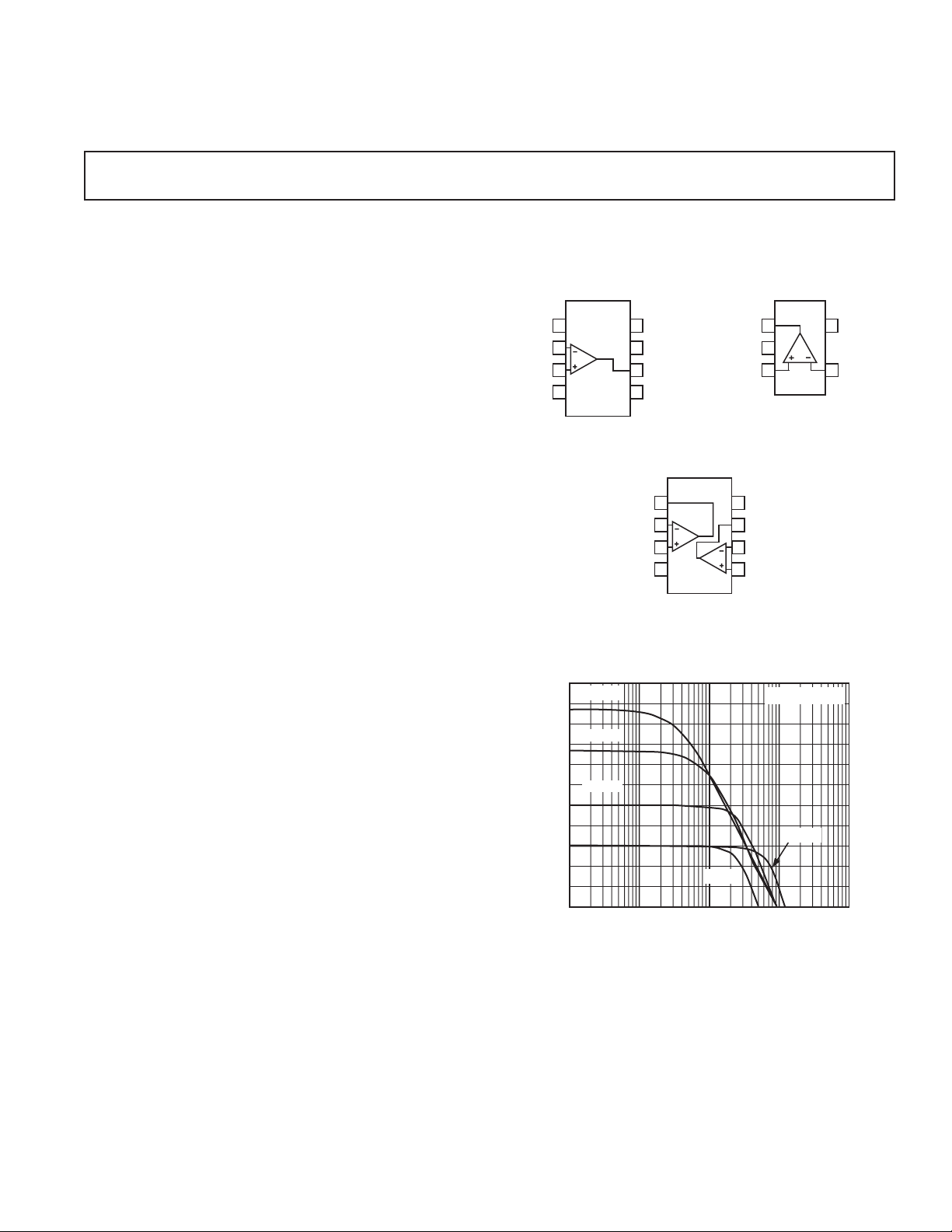
Figure 1. Small Signal Frequency Response
The AD8033 is available in small packages: SOIC-8 and SC70.
The AD8034 is also available in small packages: SOIC-8 and
SOT-23-8. They are rated to work over the industrial temperature
range of –40°C to +85°C without a premium over commercial
grade products.
One Technology Way, P.O. Box 9106, Norwood, MA 02062-9106, U.S.A.
Tel: 781/329-4700 www.analog.com
Fax: 781/326-8703 © 2003 Analog Devices, Inc. All rights reserved.

AD8033/AD8034–SPECIFICATIONS
(TA = 25ⴗC, VS = ⴞ5 V, RL = 1 k⍀, Gain = +2, unless otherwise noted.)
Parameter Conditions Min Typ Max Unit
DYNAMIC PERFORMANCE
–3 dB Bandwidth G = +1, VO = 0.2 V p-p 65 80 MHz
G = +2, V
G = +2, V
= 0.2 V p-p 30 MHz
O
= 2 V p-p 21 MHz
O
Input Overdrive Recovery Time –6 V to +6 V Input 135 ns
Output Overdrive Recovery Time –3 V to +3 V Input, G = +2 135 ns
Slew Rate (25% to 75%) G = +2, V
Settling Time to 0.1% G = +2, V
= 4 V Step 55 80 V/µs
O
= 2 V Step 95 ns
O
G = +2, VO = 8 V Step 225 ns
NOISE/HARMONIC PERFORMANCE
Distortion f
Second Harmonic R
Third Harmonic R
= 1 MHz, VO = 2 V p-p
C
= 500 Ω –82 dBc
L
= 1 kΩ –85 dBc
R
L
= 500 Ω –70 dBc
L
R
= 1 kΩ –81 dBc
L
Crosstalk, Output-to-Output f = 1 MHz, G = +2 –86 dB
Input Voltage Noise f = 100 kHz 11 nV/√Hz
Input Current Noise f = 100 kHz 0.7 fA/√Hz
DC PERFORMANCE
Input Offset Voltage VCM = 0 V 12mV
– T
T
MIN
MAX
Input Offset Voltage Match 2.5 mV
Input Offset Voltage Drift 4 27 µV/
3.5 mV
o
C
Input Bias Current 1.5 11 pA
T
MIN
– T
MAX
50 pA
Open-Loop Gain VO = ±3 V 89 92 dB
INPUT CHARACTERISTICS
Common-Mode Input Impedance 1000||2.3 GΩ||pF
Differential Input Impedance 1000||1.7 GΩ||pF
Input Common-Mode Voltage Range
FET Input Range –5.0 to +2.2 V
Usable Input Range –5.0 to +5.0 V
Common-Mode Rejection Ratio VCM = (–3 V to +1.5 V) –89 –100 dB
OUTPUT CHARACTERISTICS
Output Voltage Swing ±4.75 ±4.95 V
Output Short Circuit Current 40 mA
Capacitive Load Drive 30% Overshoot, G = +1, 35 pF
VO = 400 mV p-p
POWER SUPPLY
Operating Range 5 24 V
Quiescent Current per Amplifier 3.3 3.5 mA
Power Supply Rejection Ratio VS = ±2 V –90 –100 dB
Specifications subject to change without notice.
REV. B–2–

AD8033/AD8034
SPECIFICATIONS
(TA = 25ⴗC, VS = 5 V, RL = 1 k⍀, Gain = +2, unless otherwise noted.)
Parameter Conditions Min Typ Max Unit
DYNAMIC PERFORMANCE
–3 dB Bandwidth G = +1, VO = 0.2 V p-p 70 80 MHz
G = +2, V
G = +2, V
= 0.2 V p-p 32 MHz
O
= 2 V p-p 21 MHz
O
Input Overdrive Recovery Time –3 V to +3 V Input 180 ns
Output Overdrive Recovery Time –1.5 V to +1.5 V Input, G = +2 200 ns
Slew Rate (25% to 75%) G = +2, V
= 4 V Step 55 70 V/µs
O
Settling Time to 0.1% G = +2, VO = 2 V Step 100 ns
NOISE/HARMONIC PERFORMANCE
Distortion fC = 1 MHz, VO = 2 V p-p
Second Harmonic R
Third Harmonic R
= 500 Ω –80 dBc
L
= 1 kΩ –84 dBc
R
L
= 500 Ω –70 dBc
L
= 1 kΩ –80 dBc
R
L
Crosstalk, Output to Output f = 1 MHz, G = +2 –86 dB
Input Voltage Noise f = 100 kHz 11 nV/√Hz
Input Current Noise f = 100 kHz 0.7 fA/√Hz
DC PERFORMANCE
Input Offset Voltage VCM = 0 V 1 2.0 mV
– T
T
MIN
MAX
Input Offset Voltage Match 2.5 mV
Input Offset Voltage Drift 4 30 µV/
3.5 mV
o
C
Input Bias Current 110pA
T
MIN
– T
MAX
50 pA
Open-Loop Gain VO = 0 V to 3 V 87 92 dB
INPUT CHARACTERISTICS
Common-Mode Input Impedance 1000||2.3 GΩ||pF
Differential Input Impedance 1000||1.7 GΩ||pF
Input Common-Mode Voltage Range
FET Input Range 0 to 2.0 V
Usable Input Range 0 to 5.0 V
Common-Mode Rejection Ratio VCM = 1.0 V to 2.5 V –80 –100 dB
OUTPUT CHARACTERISTICS
Output Voltage Swing RL = 1 kΩ
0.16 to 4.83 0.04 to 4.95
V
Output Short Circuit Current 30 mA
Capacitive Load Drive 30% Overshoot, G = +1, 25 pF
VO = 400 mV p-p
POWER SUPPLY
Operating Range 5 24 V
Quiescent Current per Amplifier 3.3 3.5 mA
Power Supply Rejection Ratio VS = ±1 V –80 –100 dB
Specifications subject to change without notice.
REV. B
–3–

AD8033/AD8034
SPECIFICATIONS
(TA = 25ⴗC, VS = ⴞ12 V, RL = 1 k⍀, Gain = +2, unless otherwise noted.)
Parameter Conditions Min Typ Max Unit
DYNAMIC PERFORMANCE
–3 dB Bandwidth G = +1, VO = 0.2 V p-p 65 80 MHz
G = +2, V
G = +2, V
= 0.2 V p-p 30 MHz
O
= 2 V p-p 21 MHz
O
Input Overdrive Recovery Time –13 V to +13 V Input 100 ns
Output Overdrive Recovery Time –6.5 V to +6.5 V Input, G = +2 100 ns
Slew Rate (25% to 75%) G = +2, V
Settling Time to 0.1% G = +2, V
= 4 V Step 55 80 V/µs
O
= 2 V Step 90 ns
O
G = +2, VO = 10 V Step 225 ns
NOISE/HARMONIC PERFORMANCE
Distortion f
Second Harmonic R
Third Harmonic R
= 1 MHz, VO = 2 V p-p
C
= 500 Ω –80 dBc
L
= 1 kΩ –82 dBc
R
L
= 500 Ω –70 dBc
L
= 1 kΩ –82 dBc
R
L
Crosstalk, Output to Output f = 1 MHz, G = +2 –86 dB
Input Voltage Noise f = 100 kHz 11 nV/√Hz
Input Current Noise f = 100 kHz 0.7 fA/√Hz
DC PERFORMANCE
Input Offset Voltage V
= 0 V 1 2.0 mV
CM
– T
T
MIN
MAX
3.5 mV
Input Offset Voltage Match 2.5 mV
Input Offset Voltage Drift 4 24 µV/
Input Bias Current 2 12 pA
– T
T
MIN
MAX
50 pA
Open-Loop Gain VO = ±8 V 88 96 dB
INPUT CHARACTERISTICS
Common-Mode Input Impedance 1000||2.3 GΩ||pF
Differential Input Impedance 1000||1.7 GΩ||pF
Input Common-Mode Voltage Range
FET Input Range –12.0 to +9.0 V
Usable Input Range –12.0 to +12.0 V
Common-Mode Rejection Ratio VCM = ±5 V –92 –100 dB
OUTPUT CHARACTERISTICS
Output Voltage Swing ±11.52 ± 11.84 V
Output Short Circuit Current 60 mA
Capacitive Load Drive 30% Overshoot; G = +1 35 pF
POWER SUPPLY
Operating Range 5 24 V
Quiescent Current per Amplifier 3.3 3.5 mA
Power Supply Rejection Ratio VS = ±2 V –85 –100 dB
Specifications subject to change without notice.
o
C
ABSOLUTE MAXIMUM RATINGS*
Supply Voltage . . . . . . . . . . . . . . . . . . . . . . . . . . . . . . . . 26.4 V
Power Dissipation . . . . . . . . . . . . . . . . . . . . . . . . See Figure 2
Common-Mode Input Voltage . . . . . . . . . . . . . . . . . . . 26.4 V
Differential Input Voltage . . . . . . . . . . . . . . . . . . . . . . . . 1.4 V
Storage Temperature . . . . . . . . . . . . . . . . . . –65°C to +125°C
Operating Temperature Range . . . . . . . . . . . –40°C to +85°C
Lead Temperature Range (Soldering 10 sec) . . . . . . . . . 300°C
*Stresses above those listed under Absolute Maximum Ratings may cause perma-
nent damage to the device. This is a stress rating only; functional operation of the
device at these or any other conditions above those indicated in the operational
section of this specification is not implied. Exposure to absolute maximum rating
conditions for extended periods may affect device reliability.
REV. B–4–

AD8033/AD8034
MAXIMUM POWER DISSIPATION
The maximum safe power dissipation in the AD8033/AD8034
packages is limited by the associated rise in junction temperature
) on the die. The plastic that encapsulates the die will locally
(T
J
reach the junction temperature. At approximately 150°C, which is
the glass transition temperature, the plastic will change its properties. Even temporarily exceeding this temperature limit may change
the stresses that the package exerts on the die, permanently shifting
the parametric performance of the AD8033/AD8034. Exceeding a
junction temperature of 175°C for an extended period of time can
result in changes in silicon devices, potentially causing failure.
The still-air thermal properties of the package and PCB (
ambient temperature (T
package (P
) determine the junction temperature of the die.
D
), and the total power dissipated in the
A
),
JA
The junction temperature can be calculated as follows
TT
=+ ×()P θ
AD AJJ
The power dissipated in the package (PD) is the sum of the
quiescent power dissipation and the power dissipated in the package
due to the load drive for all outputs. The quiescent power is the
voltage between the supply pins (VS) times the quiescent current (IS).
Assuming the load (R
drive power is VS/2 I
package and some in the load (V
) is referenced to midsupply, then the total
L
some of which is dissipated in the
OUT,
OUT
I
). The difference
OUT
between the total drive power and the load power is the drive
power dissipated in the package:
P Quiescent Power Total Drive Power Load Power
=+(–)
D
PVI V V R V R
=×
[]
DSS S OUT L OUT L
+
()
[]
×
//–/2
()
2
[]
RMS output voltages should be considered. If RL is referenced
to V
, as in single-supply operation, then the total drive power
S–
I
is V
S
OUT
.
If the rms signal levels are indeterminate, consider the worst
case, when V
= VS/4 for RL to midsupply:
OUT
PVI V R
=×
()
DSS S L
+
//4
()
2
Airflow will increase heat dissipation, effectively reducing
Also, more metal directly in contact with the package leads from
metal traces, through holes, ground, and power planes will reduce
the JA. Care must be taken to minimize parasitic capacitances at
the input leads of high speed op amps as discussed in the Layout,
Grounding, and Bypassing Considerations section.
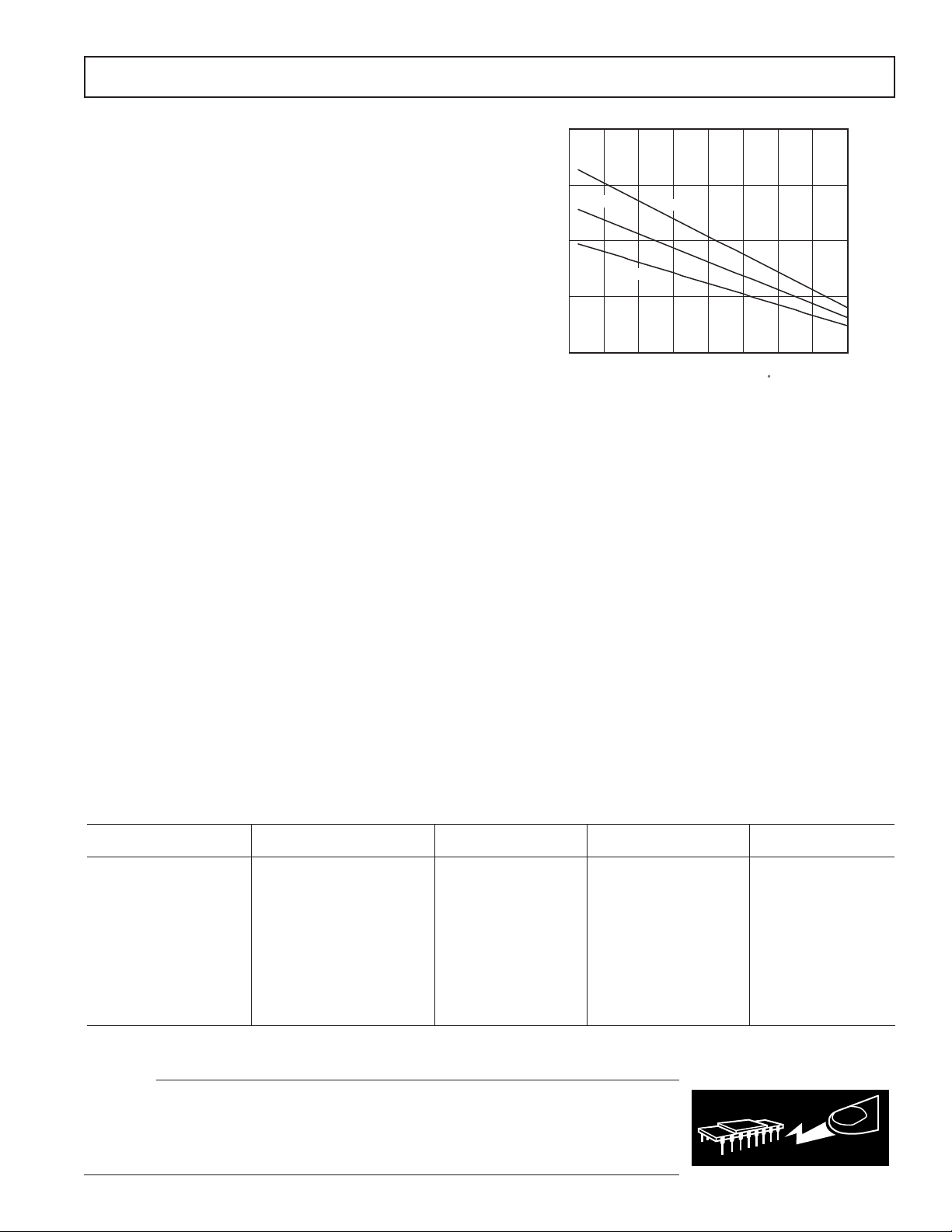
Figure 2 shows the maximum safe power dissipation in the
package versus the ambient temperature for the SOIC-8 (125°C/W),
SC70
standard 4-layer board.
OUTPUT SHORT CIRCUIT
Shorting the output to ground or drawing excessive current for
the AD8033/AD8034 will likely cause catastrophic failure.
In single-supply operation with RL referenced to VS–, worst case
= VS/2.
is V
OUT
2.0
1.5
SOT-23-8
1.0
SC70-5
0.5
MAXIMUM POWER DISSIPATION – W
0.0
–60 –40 –20 0 20 40 60 80 100
SOIC-8
AMBIENT TEMPERATURE – C
Figure 2. Maximum Power Dissipation vs.
Temperature for a Four-Layer Board
(210°C/W),
and SOT-23-8 (160°C/W) packages on a JEDEC
values are approximations.
JA
.
JA
ORDERING GUIDE
Model Temperature Range
AD8033AR +85ºC 8-Lead SOIC R-8
AD8033AR-REEL +85ºC 8-Lead SOIC R-8
AD8033AR-REEL7 +85ºC 8-Lead SOIC R-8
AD8033AKS-REEL +85ºC 5-Lead SC70 KS-5 H3B
AD8033AKS-REEL7
AD8034AR
AD8034AR-REEL7
AD8034AR-REEL
AD8034ART-REEL +85ºC 8-Lead SOT-23 RT-8
AD8034ART -REEL7 +85ºC 8-Lead SOT-23 HZA
CAUTION
ESD (electrostatic discharge) sensitive device. Electrostatic charges as high as 4000 V readily
accumulate on the human body and test equipment and can discharge without detection. Although the
AD8033/AD8034 features proprietary ESD protection circuitry, permanent damage may occur on
devices subjected to high energy electrostatic discharges. Therefore, proper ESD precautions are
recommended to avoid performance degradation or loss of functionality.
–40ºC to
–40ºC to
–40ºC to
–40ºC to
–40ºC to
–40ºC to
–40ºC to
–40ºC to
–40ºC to
–40ºC to
+85ºC 5-Lead SC70 KS-5 H3B
+85ºC 8-Lead SOIC R-8
+85ºC 8-Lead SOIC R-8
+85ºC 8-Lead SOIC R-8
REV. B
Description
–5–
Package Outline
RT-8
WARNING!
Package
Branding
Information
HZA
ESD SENSITIVE DEVICE

AD8033/AD8034–Typical Performance Characteristics
Default Conditions: ⴞ5 V, CL = 5 pF, RL = 1 k⍀, Temperature = 25ⴗC
24
G = +10
21
18
G = +5
15
12
9
G = +2
6
GAIN – dB
3
0
–3
–6
–9
0.01 1001.0 10
FREQUENCY – MHz
G = –1
VO = 200mV p-p
G = +1
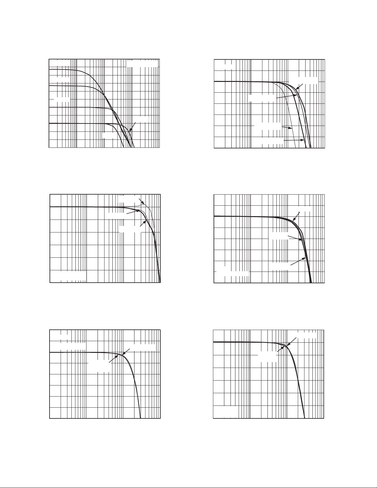
TPC 1. Small Signal Frequency Response for
Various Gains
1
0
–1
–2
–3
GAIN – dB
–4
–5
G = +1
VO = 200mV p-p
–6
0.1 100110
FREQUENCY – MHz
VS = +5V
VS = ⴞ5V
VS = ⴞ12V
TPC 2. Small Signal Frequency Response for
Various Supplies (See Test Circuit 1)
1000
8
G = +2
7
V
= 0.2V p-p
6
5
4
GAIN – dB
3
2
1
0
0.1 100110
V
= 1V p-p
OUT
= 4V p-p
V
OUT
V
= 2V p-p
OUT
FREQUENCY – MHz
OUT
TPC 4. Frequency Response for Various Output
Amplitudes (See Test Circuit 2)
8
7
6
5
4
GAIN – dB
3
2
G = +2
1
VO = 200mV p-p
0
0.1 100110
FREQUENCY – MHz
VS = ⴞ5V
V
S
VS = +5V
= ⴞ12V
TPC 5. Small Signal Frequency Response for
Various Supplies (See Test Circuit 2)
2
G = +1
1
0
–1
–2
GAIN – dB
–3
–4
–5
–6
0.1 1001
= 2V p-p
V
OUT
= ⴞ5V
V
S
= +5V
V
S
FREQUENCY – MHz
= ⴞ12V
V
10
S
TPC 3. Large Signal Frequency Response for
Various Supplies (See Test Circuit 1)
7
6
5
4
3
GAIN – dB
2
1
G = +2
VO = 2V p-p
0
0.1 100110
VS = ⴞ5V
= +5V
V
S
FREQUENCY – MHz
VS = ⴞ12V
TPC 6. Large Signal Frequency Response for
Various Supplies (See Test Circuit 2)
REV. B–6–
 Loading...