Analog Devices AD7940 Datasheet

3 mW, 100 kSPS,
FEATURES
Fast throughput rate: 100 kSPS
Specified for V
Low power
4 mW typ at 100 kSPS with 3 V supplies
17 mW typ at 100 kSPS with 5 V supplies
Wide input bandwidth:
81 dB SINAD at 10 kHz input frequency
Flexible power/serial clock speed management
No pipeline delays
High speed serial interface
SPI®/QSPI™/MICROWIRE™/DSP compatible
Standby mode: 0.5 µA max
6-Lead SOT-23 and 8-Lead MSOP packages
APPLICATIONS
Battery-powered systems
Personal digital assistants
Medical instruments
Mobile communications
Instrumentation and control systems
Remote data acquisition systems
GENERAL DESCRIPTION
The AD79401 is a 14-bit, fast, low power, successive approximation ADC. The part operates from a single 2.50 V to 5.5 V power
supply and features throughput rates up to 100 kSPS. The part
contains a low noise, wide bandwidth track-and-hold amplifier
that can handle input frequencies in excess of 7 MHz.
The conversion process and data acquisition are controlled
CS
using
with microprocessors or DSPs. The input signal is sampled on
the falling edge of
point. There are no pipelined delays associated with the part.
The AD7940 uses advanced design techniques to achieve very
low power dissipation at fast throughput rates. The reference for
the part is taken internally from V
dynamic input range to the ADC. Thus, the analog input range
for this part is 0 V to V
the SCLK frequency.
and the serial clock, allowing the devices to interface
of 2.5 V to 5.5 V
DD
CS
and the conversion is also initiated at this
, which allows the widest
DD
. The conversion rate is determined by
DD
14-Bit ADC in 6-Lead SOT-23
03305-0-001
AD7940
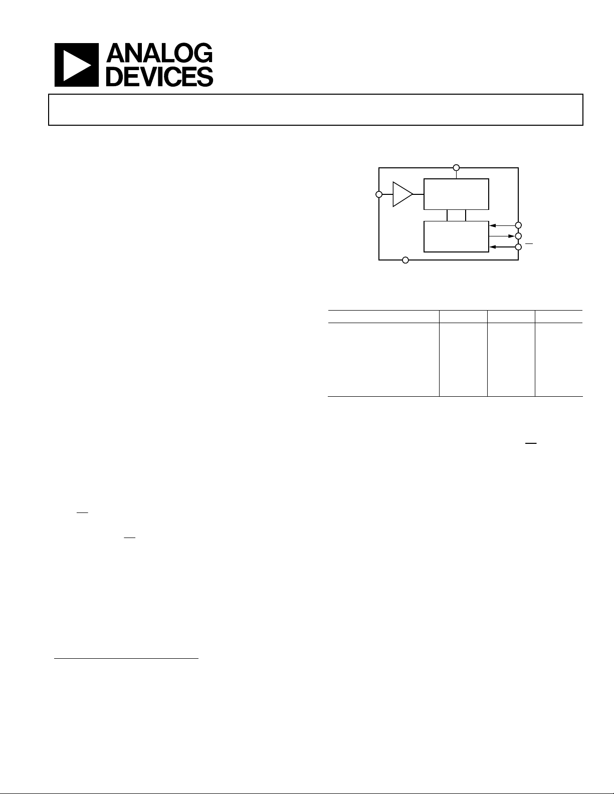
FUNCTIONAL BLOCK DIAGRAM
V
DD
GND
14-BIT SUCCESSIVE
APPROXIMATION
ADC
CONTROL
LOGIC
Figure 1.
SCLK
SDATA
CS
CS
input and
IN
T/H
AD7940
V
Table 1. 16-Bit and 14-Bit ADC (MSOP and SOT-23)
Type 100 kSPS 250 kSPS 500 kSPS
16-Bit True Differential AD7684 AD7687 AD7688
16-Bit Pseudo Differential AD7683 AD7685 AD7686
16-Bit Unipolar AD7680
14-Bit True Differential AD7944 AD7947
14-Bit Pseudo Differential AD7942 AD7946
14-Bit Unipolar AD7940
This part features a standard successive approximation ADC
with accurate control of the sampling instant via a
once off conversion control.
PRODUCT HIGHLIGHTS
1. First 14-bit ADC in a SOT-23 package.
2. High throughput with low power consumption.
3. Flexible power/serial clock speed management. The con-
version rate is determined by the serial clock, allowing the
conversion time to be reduced through the serial clock
speed increase. This allows the average power consumption
to be reduced when a power-down mode is used while not
converting. The part also features a shutdown mode to
maximize power efficiency at lower throughput rates.
Power consumption is 0.5 µA max when in shutdown.
4. Reference derived from the power supply.
5. No pipeline delay.
1
Protected by U.S. Patent No. 6,681,332.
Rev. 0
Information furnished by Analog Devices is believed to be accurate and reliable.
However, no responsibility is assumed by Analog Devices for its use, nor for any
infringements of patents or other rights of third parties that may result from its use.
Specifications subject to change without notice. No license is granted by implication
or otherwise under any patent or patent rights of Analog Devices. Trademarks and
registered trademarks are the property of their respective owners.
One Technology Way, P.O. Box 9106, Norwood, MA 02062-9106, U.S.A.
Tel: 781.329.4700
Fax: 781.326.8703 © 2004 Analog Devices, Inc. All rights reserved.
www.analog.com

AD7940
TABLE OF CONTENTS
Specifications..................................................................................... 3
Normal Mode.............................................................................. 13
Timing Specifications....................................................................... 5
Absolute Maximum Ratings............................................................ 6
ESD Caution.................................................................................. 6
Pin Configurations and Function Descriptions ........................... 7
Terminology ...................................................................................... 8
Typical Performance Characteristics ............................................. 9
Circuit Information........................................................................ 11
Converter Operation.................................................................. 11
Analog Input............................................................................... 11
ADC Transfer Function................................................................. 12
Typical Connection Diagram ................................................... 12
Modes of Operation .......................................................................13
REVISION HISTORY
6/04—Revision 0: Initial Version
Power-Down Mode.................................................................... 14
Power vs. Throughput Rate........................................................... 15
Serial Interface ................................................................................ 16
Microprocessor Interfacing........................................................... 17
AD7940 to TMS320C541.......................................................... 17
AD7940 to ADSP-218x.............................................................. 17
AD7940 to DSP563xx................................................................ 18
Application Hints ........................................................................... 19
Grounding and Layout .............................................................. 19
Evaluating the AD7940 Performance ...................................... 19
Outline Dimensions....................................................................... 20
Ordering Guide .......................................................................... 20
Rev. 0 | Page 2 of 20

AD7940
SPECIFICATIONS
VDD = 2.50 V to 5.5 V, f
Table 2.
Parameter B Version1 Unit Test Conditions/Comments
DYNAMIC PERFORMANCE fIN = 10 kHz sine wave
Signal-to-Noise + Distortion (SINAD)
Total Harmonic Distortion (THD)2 −98 dB typ
Peak Harmonic or Spurious Noise (SFDR)
Intermodulation Distortion (IMD)2
Second-Order Terms −94 dB typ
Third-Order Terms −100 dB typ
Aperture Delay 20 ns max
Aperture Jitter 30 ps typ
Full Power Bandwidth 7 MHz typ @ −3 dB
2 MHz typ @ −0.1 dB
DC ACCURACY
Resolution 14 Bits min VDD = 2.5 V to 4.096 V
13 Bits min VDD > 4.096 V
Integral Nonlinearity2 ±1 LSB max VDD = 2.5 V to 4.096 V
±2 LSB max VDD > 4.096 V
Offset Error2 ±6 LSB max
Gain Error2 ±8 LSB max
ANALOG INPUT
Input Voltage Ranges 0 to V
DC Leakage Current ±0.3 µA max
Input Capacitance 30 pF typ
LOGIC INPUTS
Input High Voltage, V
Input Low Voltage, V
0.8 V max VDD = 5 V
Input Current, IIN ±0.3 µA max Typically 10 nA, VIN = 0 V or V
Input Capacitance, C
LOGIC OUTPUTS
Output High Voltage, VOH VDD – 0.2 V min I
Output Low Voltage, V
Floating-State Leakage Current ±0.3 µA max
Floating-State Output Capacitance
Output Coding Straight (Natural) Binary
CONVERSION RATE
Conversion Time 8 µs max 16 SCLK cycles
Track-and-Hold Acquisition Time 500 ns max Full-scale step input
400 ns max Sine wave input ≤ 10 kHz
Throughput Rate 100 kSPS max See the Serial Interface section
POWER REQUIREMENTS
V
DD
IDD Digital I/PS = 0 V or V
Normal Mode (Static) 5.2 mA max VDD = 5.5 V; SCLK on or off
2 mA max VDD = 3.6 V; SCLK on or off
Normal Mode (Operational) 4.8 mA max VDD = 5.5 V; f
1.9 mA max VDD = 3.6 V; f
Full Power-Down Mode 0.5 µA max SCLK on or off. VDD = 5.5 V
0.3 µA max SCLK on or off. VDD = 3.6 V
1
= 2.5 MHz, f
SCLK
INH
INL
2, 3
IN
OL
= 100 kSPS, unless otherwise noted; TA = T
SAMPLE
2
2
81 dB min
−95 dB typ
DD
2.4 V min
0.4 V max VDD = 3 V
10 pF max
0.4 V max I
2, 3
10 pF max
2.50/5.5 V min/V max
MIN
to T
, unless otherwise noted.
MAX
V
= 200 µA; VDD = 2.50 V to 5.25 V
SOURCE
= 200 µA
SINK
SAMPLE
SAMPLE
DD
DD
= 100 kSPS; 3.3 mA typ
= 100 kSPS; 1.29 mA typ
Rev. 0 | Page 3 of 20

AD7940
Parameter B Version1 Unit Test Conditions/Comments
Power Dissipation
Normal Mode (Operational) 26.4 mW max VDD = 5.5 V; f
6.84 mW max VDD = 3.6 V; f
Full Power-Down 2.5 µW max VDD = 5.5 V
1.08 µW max VDD = 3.6 V
1
Temperature range for B Version is –40°C to +85°C.
2
See the section. Terminology
3
Sample tested at initial release to ensure compliance.
4
See the section. Power vs. Throughput Rate
4
V
= 5.5 V
DD
SAMPLE
SAMPLE
= 100 kSPS
= 100 kSPS
Rev. 0 | Page 4 of 20

AD7940
TIMING SPECIFICATIONS
Sample tested at initial release to ensure compliance. All input signals are specified with tr = tf = 5 ns (10% to 90% of VDD) and timed from
a voltage level of 1.6 V.
= 2.50 V to 5.5 V; TA = T
V
DD
MIN
to T
, unless other wise noted.
MAX
Table 3.
Limit at T
MIN
, T
MAX
Parameter 3 V 5 V Unit Description
1
f
SCLK
250 250 kHz min
2.5 2.5 MHz max
t
16 × t
CONVERT
t
50 50 ns min
QUIET
16 × t
SCLK
min
SCLK
Minimum quiet time required between bus relinquish and start of
next conversion
t1 10 10 ns min
t2 10 10 ns min
2
t
3
2
t
120 80 ns max Data access time after SCLK falling edge
4
t5 0.4 t
t6 0.4 t
48 35 ns max
0.4 t
SCLK
0.4 t
SCLK
ns min SCLK low pulse width
SCLK
SCLK
ns min SCLK high pulse width
Minimum
CS
Delay from
CS
pulse width
to SCLK setup time
CS
until SDATA three-state disabled
t7 10 10 ns min SCLK to data valid hold time
3
t
8
t
POWER-UP
4
45 35 ns max SCLK falling edge to SDATA high impedance
1 1 µs typ Power up time from full power-down
1
Mark/space ratio for the SCLK input is 40/60 to 60/40.
2
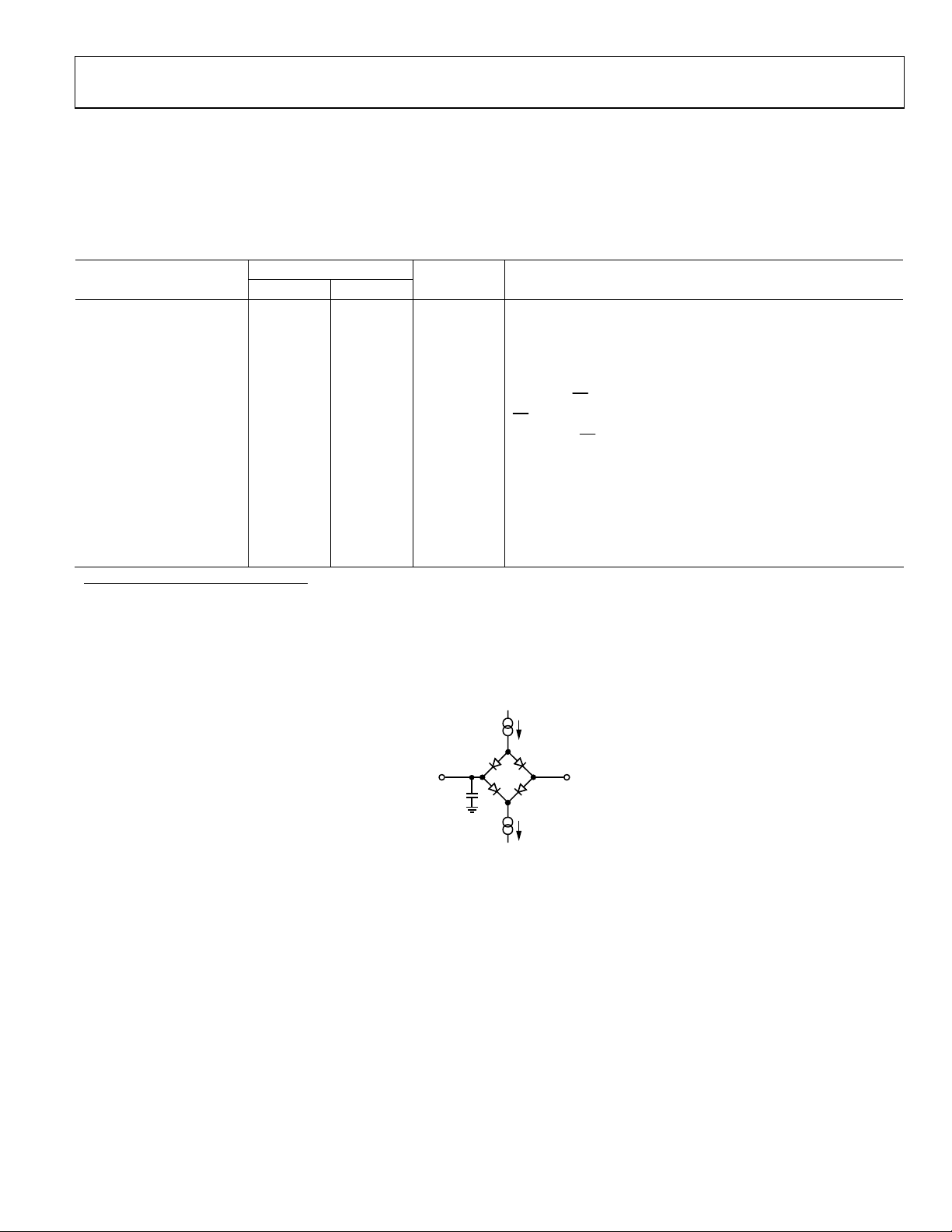
Measured with the load circuit of and defined as the time required for the output to cross 0.8 V or 2.0 V. Figure 2
3
t8 is derived form the measured time taken by the data outputs to change 0.5 V when loaded with the circuit of The measured number is then extrapolated
back to remove the effects of charging or discharging the 50 pF capacitor. This means that the time, t
time of the part and is independent of the bus loading.
4
See the section. Power vs. Throughput Rate
8
Figure 2.
, quoted in the timing characteristics is the true bus relinquish
TO OUTPUT
PIN
200µAI
C
L
50pF
200µAI
OL
1.6V
OH
03305-0-002
Figure 2. Load Circuit for Digital Output Timing Specification
Rev. 0 | Page 5 of 20

AD7940
ABSOLUTE MAXIMUM RATINGS
TA = 25°C, unless otherwise noted.
Table 4.
Parameter Rating
VDD to GND −0.3 V to +7 V
Analog Input Voltage to GND −0.3 V to VDD + 0.3 V
Digital Input Voltage to GND −0.3 V to +7 V
Digital Output Voltage to GND −0.3 V to VDD + 0.3 V
Input Current to Any Pin Except Supplies1 ±10 mA
Operating Temperature Range
Commercial (B Version) −40°C to +85°C
Storage Temperature Range −65°C to +150°C
Junction Temperature 150°C
SOT-23 Package, Power Dissipation 450 mW
θJA Thermal Impedance 229.6°C/W
θJC Thermal Impedance 91.99°C/W
MSOP Package, Power Dissipation 450 mW
θJA Thermal Impedance 205.9°C/W
θJC Thermal Impedance 43.74°C/W
Lead Temperature, Soldering
Vapor Phase (60 secs) 215°C
Infared (15 secs) 220°C
ESD 4 kV
Stresses above those listed under Absolute Maximum Ratings
may cause permanent damage to the device. This is a stress rating only; functional operation of the device at these or any
other conditions above those listed in the operational sections
of this specification is not implied. Exposure to absolute maximum rating conditions for extended periods may affect device
reliability.
1
Transient currents of up to 100 mA will not cause SCR latch-up.
ESD CAUTION
ESD (electrostatic discharge) sensitive device. Electrostatic charges as high as 4000 V readily accumulate on the
human body and test equipment and can discharge without detection. Although this product features
proprietary ESD protection circuitry, permanent damage may occur on devices subjected to high energy
electrostatic discharges. Therefore, proper ESD precautions are recommended to avoid performance
degradation or loss of functionality.
Rev. 0 | Page 6 of 20
 Loading...