

Four-Channel, Simultaneous
a
FEATURES
Fast (2.4 s) 14-Bit ADC
Four Simultaneously Sampled Inputs
Four Track/Hold Amplifiers
0.35 s Track/Hold Acquisition Time
2.4 s Conversion Time per Channel
HW/SW Select of Channel Sequence for Conversion
Single Supply Operation
Selection of Input Ranges: 10 V, 5 V and 2.5 V,
0 V to 5 V and 0 V to 2.5 V
High Speed Parallel Interface Which Also Allows
Interfacing to 3 V Processors
Low Power, 115 mW Typ
Power Saving Mode, 15 W Typ
Overvoltage Protection on Analog Inputs
APPLICATIONS
AC Motor Control
Uninterruptible Power Supplies
Industrial Power Meters/Monitors
Data Acquisition Systems
Communications
STBY
V
IN1A
V
IN1B
V
IN2A
V
IN2B
V
IN3A
V
IN3B
V
IN4A
V
IN4B
FRSTDATA
BUSY
EOC
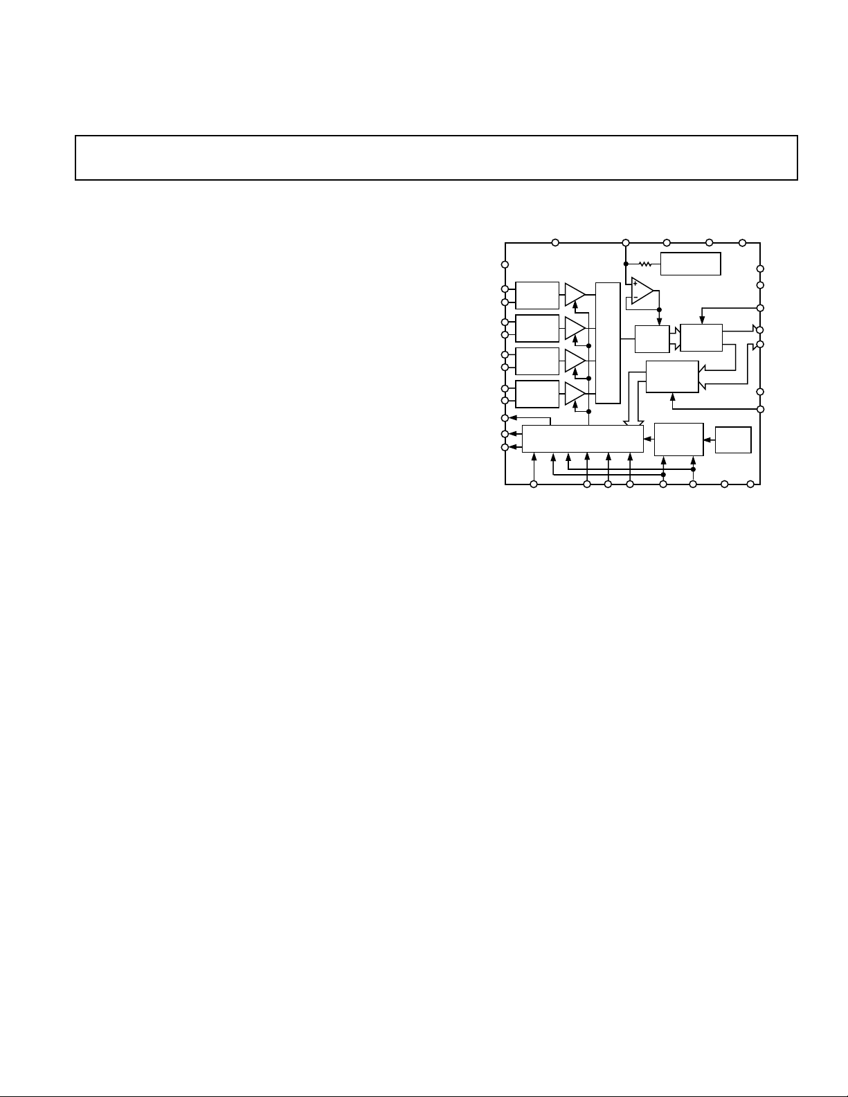
Sampling, Fast, 14-Bit ADC
AD7865
FUNCTIONAL BLOCK DIAGRAM
V
+2.5V
REFERENCE
OUTPUT
SELECT
INT/EXT
CLOCK
SELECT
INT/EXT
CLK/SL2
DV
DD
AD7865
LATCH
DB0–DB3
AGND
DRIVE
INT
CLOCK
AGND
DGND
AGND
RD
DB13
DB0
CS
WR
SIGNAL
SCALING
SIGNAL
SCALING
SIGNAL
SCALING
SIGNAL
SCALING
CONVST
AV
DD
TRACK/HOLD
4
MUX
CONVERSION
CONTROL LOGIC
SL3 SL4
V
V
REF
REFAGND
6k
14-BIT
ADC
CHANNEL
REGISTER
CLK IN
H/S
/SL1
SEL
GENERAL DESCRIPTION
The AD7865 is a fast, low power, four-channel simultaneous
sampling 14-bit A/D converter that operates from a single 5 V
supply. The part contains a 2.4 µs successive approximation
ADC, four track/hold amplifiers, 2.5 V reference, on-chip clock
oscillator, signal conditioning circuitry and a high speed parallel
interface. The input signals on four channels are sampled simultaneously thus preserving the relative phase information of the
signals on the four analog inputs. The part accepts analog input
ranges of ±10 V, ±5 V, ± 2.5 V, 0 V to 2.5 V and 0 V to 5 V.
The part allows any subset of the four channels to be converted
in order to maximize the throughput rate on the selected sequence.
The channels to be converted can be selected either via hardware (channel select input pins) or via software (programming
the channel select register).
A single conversion start signal (CONVST) simultaneously places
all the track/holds into hold and initiates conversion sequence
for the selected channels. The EOC signal indicates the end of
each individual conversion in the selected conversion sequence.
The BUSY signal indicates the end of the conversion sequence.
Data is read from the part via a 14-bit parallel data bus using the
standard CS and RD signals. Maximum throughput for a single
channel is 350 kSPS. For all four channels the maximum throughput is 100 kSPS.
The AD7865 is available in a small (0.3 sq. inch area) 44-lead
PQFP.
PRODUCT HIGHLIGHTS
1. The AD7865 features four Track/Hold amplifiers and a fast
(2.4 µs) ADC allowing simultaneous sampling and then con-
version of any subset of the four channels.
2. The AD7865 operates from a single 5 V supply and consumes only 115 mW typ, making it ideal for low power and
portable applications.
3. The part offers a high speed parallel interface for easy connection to microprocessors, microcontrollers and digital
signal processors.
4. The part is offered in three versions with different analog
input ranges. The AD7865-1 offers the standard industrial
ranges of ±10 V and ± 5 V; the AD7865-2 offers a unipolar
range of 0 V to 2.5 V or 0 V to 5 V and the AD7865-3 offers
the common signal processing input range of ±2.5 V.
5. The part features very tight aperture delay matching between
the four input sample and hold amplifiers.
REV. B
Information furnished by Analog Devices is believed to be accurate and
reliable. However, no responsibility is assumed by Analog Devices for its
use, nor for any infringements of patents or other rights of third parties
which may result from its use. No license is granted by implication or
otherwise under any patent or patent rights of Analog Devices.
One Technology Way, P.O. Box 9106, Norwood, MA 02062-9106, U.S.A.
Tel: 781/329-4700 World Wide Web Site: http://www.analog.com
Fax: 781/326-8703 © Analog Devices, Inc., 2000

AD7865–SPECIFICATIONS
(VDD = 5 V 5%, AGND = DGND = 0 V, V
cations T
MIN
to T
unless otherwise noted.)
MAX
= Internal. Clock = Internal; all specifi-
REF
Parameter A, Y Versions1B Version Unit Test Conditions/Comments
SAMPLE AND HOLD
–3 dB Full Power Bandwidth 3 3 MHz typ
Aperture Delay 20 20 ns max
Aperture Jitter 50 50 ps typ
Aperture Delay Matching 4 4 ns max
DYNAMIC PERFORMANCE
2
Signal to (Noise + Distortion) Ratio
3
fIN = 100 kHz, fS = 350 kSPS
@ 25°C
AD7865-1, AD7865-3 78 78 dB min Typically 80 dB
AD7865-2 77 77 dB min Typically 78 dB
to T
T
MIN
MAX
AD7865-1, AD7865-3 77 77 dB min
AD7865-2 76 76 dB min
Total Harmonic Distortion
Peak Harmonic or Spurious Noise
Intermodulation Distortion
3, 4
3
–86 –86 dB max
3, 4
–86 –86 dB max
fa = 49 kHz, fb = 50 kHz
2nd Order Terms –95 –95 dB typ
3rd Order Terms –95 –95 dB typ
Channel-to-Channel Isolation
3, 5
–88 –88 dB max fIN = 50 kHz Sine Wave
DC ACCURACY Any Channel
Resolution 14 14 Bits
Relative Accuracy (INL)
Differential Nonlinearity (DNL)
AD7865-1
Positive Gain Error
Positive Gain Error Match
Negative Gain Error
Negative Gain Error Match
3
3
3
3
3
3
± 2 ± 1.5 LSB max Typically 0.6 LSBs
± 1 ± 1 LSB max No Missing Codes Guaranteed
± 10 ± 8 LSB max Typically ±2 LSBs
8 8 LSB max Typically 2 LSBs
± 10 ± 8 LSB max Typically ±2 LSBs
8 8 LSB max Typically 2 LSBs
Bipolar Zero Error ±12 ± 10 LSB max Typically ±2 LSBs
Bipolar Zero Error Match 6 6 LSB max Typically 1.5 LSBs
AD7865-2
Positive Gain Error
Positive Gain Error Match
Unipolar Offset Error
Unipolar Offset Error Match
AD7865-3
Positive Gain Error
Positive Gain Error Match
Negative Gain Error
Negative Gain Error Match
3
3
3
3
3
3
3
3
± 16 ± 16 LSB max Typically ±2 LSBs
8 8 LSB max Typically 2 LSBs
± 10 ± 10 LSB max Typically ±2 LSBs
10 10 LSB max Typically 2 LSBs
± 16 ± 14 LSB max Typically ±6 LSBs
8 8 LSB max Typically 2 LSBs
± 16 ± 14 LSB max Typically ±6 LSBs
8 8 LSB max Typically 2 LSBs
Bipolar Zero Error ±14 ± 12 LSB max Typically ±5 LSBs
Bipolar Zero Error Match 8 6 LSB max Typically 2 LSBs
ANALOG INPUTS
AD7865-1
Input Voltage Range ± 5, ± 10 ± 5, ± 10 Volts
Input Current 1, 1 1, 1 mA max VIN = –5 V and –10 V Respectively,
Typically 0.7 mA
AD7865-2
Input Voltage Range 0 V to 2.5 V, 0 V to 2.5 V,
0 V to 5 V 0 V to 5 V Volts
Input Current 10 10 µA max V
1 1 mA max V
= 2.5 V, 0 V to 2.5 V Range, Typ 1 µA
IN
= 5 V, 0 V to 5 V Range, Typ 0.7 mA
IN
AD7865-3
Input Voltage Range ± 2.5 ± 2.5 Volts
Input Current 1 1 mA max VIN = –2.5 V, Typically 0.7 mA
–2–
REV. B

Parameter A, Y Versions1B Version Unit Test Conditions/Comments
REFERENCE INPUT/OUTPUT
V
IN Input Voltage Range 2.375/2.625 2.375/2.625 V
REF
IN Input Capacitance
V
REF
V
OUT Output Voltage 2.5 2.5 V nom
REF
OUT Error @ 25°C ± 10 ±10 mV max
V
REF
OUT Error T
V
REF
V
OUT Temperature Coefficient 25 25 ppm/°C typ
REF
V
OUT Output Impedance 6 6 kΩ typ See Reference Section
REF
MIN
to T
6
MAX
10 10 pF max
± 20 ± 20 mV max
MIN/VMAX
2.5 V ± 5%
LOGIC INPUTS
Input High Voltage, V
Input Low Voltage, V
Input Current, I
Input Capacitance, C
INL
IN
IN
INH
6
2.4 2.4 V min VDD = 5 V ± 5%
0.8 0.8 V max VDD = 5 V ± 5%
± 10 ± 10 µA max
10 10 pF max
LOGIC OUTPUTS
Output High Voltage, V
Output Low Voltage, V
OL
OH
4.0 4.0 V min I
0.4 0.4 V max I
SOURCE
= 1.6 mA
SINK
= 400 µA
DB13–DB0
High Impedance
Leakage Current ± 10 ± 10 µA max
Capacitance
6
10 10 pF max
Output Coding
AD7865-1, AD7865-3 Two’s Complement
AD7865-2 Straight (Natural) Binary
CONVERSION RATE
Conversion Time 2.4 2.4 µs max For Single Channel
Track/Hold Acquisition Time
2, 3
0.35 0.35 µs max
Throughput Time 350 350 kSPS max For Single Channel
100 100 kSPS max For All Four Channels
POWER REQUIREMENTS
V
DD
I
DD
5 5 V nom ±5% for Specified Performance
AD7865-1 Typically 23 mA, Logic Inputs = 0 V or V
Normal Mode 32 32 mA max
Standby Mode 20 20 µA max
AD7865-2 Typically 20 mA, Logic Inputs = 0 V or V
Normal Mode 30 30 mA max
Standby Mode 20 20 µA max
AD7865-3 Typically 23 mA, Logic Inputs = 0 V or V
Normal Mode 32 32 mA max
Standby Mode 20 20 µA max
Power Dissipation
AD7865-1
Normal Mode 160 160 mW max Typically 115 mW. V
DD
= 5 V
Standby Mode 100 100 µW max Typically 15 µW
AD7865-2
Normal Mode 150 150 mW max Typically 100 mW. V
DD
= 5 V
Standby Mode 100 100 µW max Typically 15 µW
AD7865-3
Normal Mode 160 160 mW max Typically 115 mW. V
DD
= 5 V
Standby Mode 100 100 µW max Typically 15 µW
NOTES
1
Temperature ranges are as follows : A, B Versions: –40°C to +85°C, Y Version: –40°C to +105°C.
2
Performance measured through full channel (SHA and ADC).
3
See Terminology.
4
Total Harmonic Distortion and Peak Harmonic or Spurious Noise are specified at –83 dBs for the AD7865-2.
5
Measured between any two channels with the other two channels grounded.
6
Sample tested @ 25°C to ensure compliance.
Specifications subject to change without notice.
AD7865
DD
DD
DD
REV. B
–3–
AD7865
TIMING CHARACTERISTICS
(VDD = 5 V 5%, AGND = DGND = 0 V, V
1, 2
T
to T
MIN
unless otherwise noted.)
MAX
= Internal, Clock = Internal; all specifications
REF
Parameter A, B, Y Versions Unit Test Conditions/Comments
t
CONV
2.4 µs max Conversion Time, Internal Clock
3.2 µs max Conversion Time, External Clock (5 MHz)
t
ACQ
t
BUSY
t
WAKE-UP
t
1
t
2
—External V
REF
3
0.35 µs max Acquisition Time
No. of Channels Selected Number of Channels Multiplied by t
× (t
) µs max
CONV
CONV
1 µs max STBY Rising Edge to CONVST Rising Edge
35 ns min CONVST Pulsewidth
70 ns min CONVST Rising Edge to BUSY Rising Edge
Read Operation
t
3
t
4
t
5
4
t
6
5
t
7
0 ns min CS to RD Setup Time
0 ns min CS to RD Hold Time
35 ns min Read Pulsewidth
35 ns max Data Access Time after Falling Edge of RD, V
40 ns max Data Access Time after Falling Edge of RD, V
5 ns min Bus Relinquish Time after Rising Edge of RD
DRIVE
DRIVE
= 5 V
= 3 V
30 ns max
t
8
t
9
15 ns min Time Between Consecutive Reads
120 ns min EOC Pulsewidth
180 ns max
t
10
t
11
t
12
70 ns max RD Rising Edge to FRSTDATA Edge (Rising or Falling)
15 ns max EOC Falling Edge to FRSTDATA Falling Delay
0 ns min EOC to RD Delay
Write Operation
t
13
t
14
t
15
t
16
t
17
20 ns min WR Pulsewidth
0 ns min CS to WR Setup Time
0 ns min WR to CS Hold Time
5 ns min Input Data Setup Time of Rising Edge of WR
5 ns min Input Data Hold Time
External Clock
t
18
NOTES
1
Sample tested at 25°C to ensure compliance. All input signals are measured with tr = tf = 1 ns (10% to 90% of 5 V) and timed from a voltage level of 1.6 V.
2
See Figures 6, 7 and 8.
3
Refer to the Standby Mode Operation section. The MAX specification of 1 µs is valid when using a 0.1 µF decoupling capacitor on the V
4
Measured with the load circuit of Figure 1 and defined as the time required for an output to cross 0.8 V or 2.4 V.
5
These times are derived from the measured time taken by the data outputs to change 0.5 V when loaded with the circuit of Figure 1. The measured number is then
extrapolated back to remove the effects of charging or discharging the 50 pF capacitor. This means that the times quoted in the timing characteristics are the true bus
relinquish times of the part and as such are independent of external bus loading capacitances.
Specifications subject to change without notice.
200 ns min CONVST Falling Edge to CLK Rising Edge
pin.
REF
1.6mA
TO OUTPUT
PIN
50pF
400A
1.6V
Figure 1. Load Circuit for Access Time and Bus Relinquish Time
–4–
REV. B
AD7865
WARNING!
ESD SENSITIVE DEVICE
12 1 3 14 15 16 17 18 192021 22
3
4
5
6
7
1
2
10
11
8
9
40 39 3841
42
4344 36 35 3437
PIN 1
IDENTIFIER
TOP VIEW
(Not to Scale)
29
30
31
32
27
28
25
26
23
24
33
DB7
DB8
DB0
DB1
DB2
DB3
DB4
DB5
DGND
V
DRIVE
DV
DD
DB6
EOC
DB9
DB10
DB12
DB13
AGND
AGND
AGND
V
I
N4B
V
IN4A
V
IN3B
V
IN3A
V
IN2B
BUSY
FRSTDATA
CONVST
CS
RD
WR
CLK IN/SL1
INT/EXT CLK/SL2
SL3
SL4
H/S SEL
AV
DD
V
REF
AGND
V
I
N2A
V
IN1B
V
I
N1A
STBY
AD7865
DB11
ABSOLUTE MAXIMUM RATINGS*
(TA = 25°C unless otherwise noted)
VDD to AGND . . . . . . . . . . . . . . . . . . . . . . . . . –0.3 V to +7 V
to DGND . . . . . . . . . . . . . . . . . . . . . . . . . –0.3 V to +7 V
V
DD
V
to DGND . . . . . . . . . . . . . . . . . . . . . . . . . VDD + 0.3 V
DRIVE
Analog Input Voltage to AGND
AD7865-1 (± 10 V Input Range) . . . . . . . . . . . . . . . . ±18 V
AD7865-1 (± 5 V Input Range) . . . . . . . . . . . . . . . . . . ± 9 V
AD7865-2 . . . . . . . . . . . . . . . . . . . . . . . . . . . –1 V to +18 V
AD7865-3 . . . . . . . . . . . . . . . . . . . . . . . . . . . –4 V to +18 V
Reference Input Voltage to AGND . . . –0.3 V to V
Digital Input Voltage to DGND . . . . . –0.3 V to V
Digital Output Voltage to DGND . . . . –0.3 V to V
+ 0.3 V
DD
+ 0.3 V
DD
+ 0.3 V
DD
Operating Temperature Range
Commercial (A, B Versions) . . . . . . . . . . . –40°C to +85°C
Automotive (Y Version) . . . . . . . . . . . . . . –40°C to +105°C
Storage Temperature Range . . . . . . . . . . . . –65°C to +150°C
Junction Temperature . . . . . . . . . . . . . . . . . . . . . . . . . 150°C
PQFP Package, Power Dissipation . . . . . . . . . . . . . . 450 mW
Thermal Impedance . . . . . . . . . . . . . . . . . . . . . 95°C/W
θ
JA
Lead Temperature, Soldering
Vapor Phase (60 sec) . . . . . . . . . . . . . . . . . . . . . . 215°C
Infrared (15 sec) . . . . . . . . . . . . . . . . . . . . . . . . . . 220°C
*Stresses above those listed under Absolute Maximum Ratings may cause perma-
nent damage to the device. This is a stress rating only; functional operation of the
device at these or any other conditions above those listed in the operational
sections of this specification is not implied. Exposure to absolute maximum rating
conditions for extended periods may affect device reliability.
ORDERING GUIDE
Input Relative Temperature Package Package
Model Ranges Accuracy Ranges Description Option
AD7865AS-1 ± 5 V, ±10 V ± 2 LSB –40°C to +85°C Plastic Lead Quad Flatpack S-44
AD7865BS-1 ± 5 V, ± 10 V ± 1.5 LSB – 40°C to +85°C Plastic Lead Quad Flatpack S-44
AD7865YS-1 ± 5 V, ±10 V ± 2 LSB –40°C to +105°C Plastic Lead Quad Flatpack S-44
AD7865AS-2 0 V to 2.5 V, 0 V to 5 V ± 2 LSB –40°C to +85°C Plastic Lead Quad Flatpack S-44
AD7865BS-2 0 V to 2.5 V, 0 V to 5 V ± 1.5 LSB – 40°C to +85°C Plastic Lead Quad Flatpack S-44
AD7865YS-2 0 V to 2.5 V, 0 V to 5 V ± 2 LSB –40°C to +105°C Plastic Lead Quad Flatpack S-44
AD7865AS-3 ± 2.5 V ± 2 LSB –40°C to +85°C Plastic Lead Quad Flatpack S-44
AD7865BS-3 ± 2.5 V ± 1.5 LSB –40°C to +85°C Plastic Lead Quad Flatpack S-44
AD7865YS-3 ± 2.5 V ± 2 LSB –40°C to +105°C Plastic Lead Quad Flatpack S-44
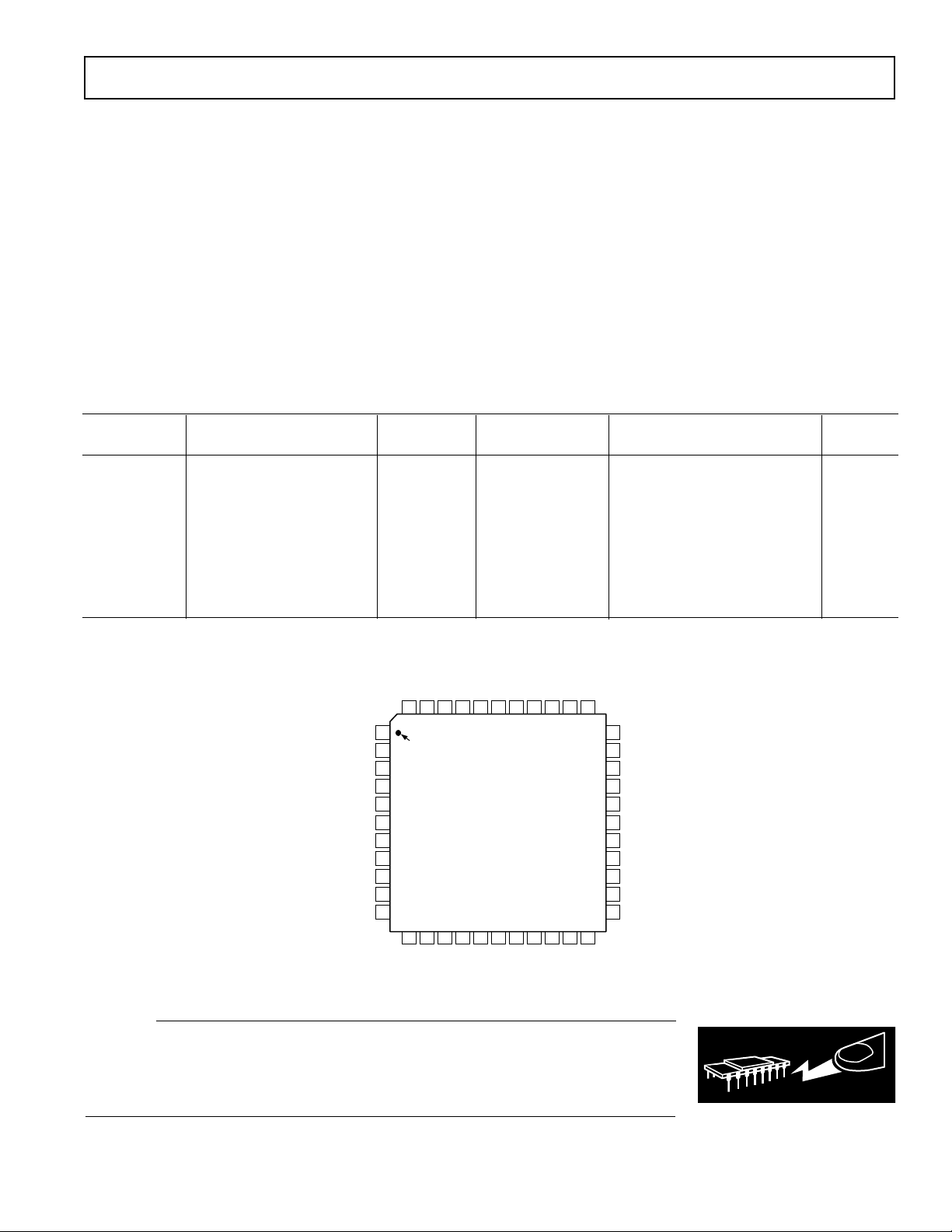
PIN CONFIGURATION
–5–
CAUTION
ESD (electrostatic discharge) sensitive device. Electrostatic charges as high as 4000 V readily
accumulate on the human body and test equipment and can discharge without detection.
Although the AD7865 features proprietary ESD protection circuitry, permanent damage may
occur on devices subjected to high-energy electrostatic discharges. Therefore, proper ESD
precautions are recommended to avoid performance degradation or loss of functionality.
REV. B

AD7865
PIN FUNCTION DESCRIPTIONS
Pin Mnemonic Description
1 BUSY Busy Output. The busy output is triggered high by the rising edge of CONVST and remains
high until conversion is completed on all selected channels.
2 FRSTDATA First Data Output. FRSTDATA is a logic output which, when high, indicates that the Output
Data Register Pointer is addressing Register 1—See Accessing the Output Data Registers.
3 CONVST Convert Start Input. Logic Input. A low-to-high transition on this input puts all track/holds
into their hold mode and starts conversion on the selected channels. In addition, the state of
the Channel Sequence Selection is also latched on the rising edge of CONVST.
4 CS Chip Select Input. Active low logic input. The device is selected when this input is active.
5 RD Read Input. Active low logic input which is used in conjunction with CS low to enable the
data outputs. Ensure the WR pin is at logic high while performing a read operation.
6 WR Write Input. A rising edge on the WR input, with CS low and RD high, latches the logic state
on DB0 to DB3 into the channel select register.
7 CLK IN/SL1 Conversion Clock Input/Hardware Channel Select. The function of this pin depends upon the
H/S SEL input. When the H/S SEL input is high (choosing software control of the channel
selection sequence), this pin assumes its CLK IN function. CLK IN is an externally applied
clock (that is only necessary when INT/EXT CLK is high) this allows the user to control the
conversion rate of the AD7865. Each conversion needs 16 clock cycles in order for the conver-
sion to be completed. The clock should have a duty cycle that is no greater than 60/40. See
Using an External Clock.
When the H/S SEL input is low (choosing hardware control of the channel conversion se-
quence), this pin assumes its Hardware Channel Select function. The SL1 input determines
whether Channel 1 is included in the channel conversion sequence. The selection is latched
on the rising edge of CONVST. See Selecting a Conversion Sequence.
8 INT/EXT CLK/SL2 Internal/External Clock/Hardware Channel Select. The function of this pin depends upon the
H/S SEL input. When the H/S SEL input is high (choosing software control of the channel
selection sequence), this pin assumes its INT/EXT CLK function. When INT/EXT CLK is at
a Logic 0, the AD7865 uses its internally generated master clock. When INT/EXT CLK is at
Logic 1, the master clock is generated externally to the device and applied to CLK IN.
When the H/S SEL input is low (choosing hardware control of the channel conversion sequence),
this pin assumes its Hardware Channel Select function. The SL2 input determines whether
Channel 2 is included in the channel conversion sequence. The selection is latched on the
rising edge of CONVST. When H/S is at Logic 1 these pins have no function and can be tied
to Logic 1 or Logic 0. See Selecting a Conversion Sequence.
9, 10 SL3, SL4 Hardware Channel Select. When the H/S SEL input is at Logic 0, the SL3 input determines
whether Channel 3 is included in the channel conversion sequence while SL4 determines
whether Channel 4 is included in the channel conversion sequence. When the pin is at Logic
1, the channel is included in the conversion sequence. When the pin is at Logic 0, the channel
is excluded from the conversion sequence. The selection is latched on the rising edge of
CONVST. See Selecting a Conversion Sequence.
11 H/S SEL Hardware/Software Select Input. When this pin is at a Logic 0, the AD7865 conversion
sequence selection is controlled via the SL1–SL4 input pins and runs off an internal clock.
When this pin is at Logic 1, the conversion sequence is controlled via the channel select regis-
ter and allows the ADC to run with an internal or external clock. See Selecting a Conversion
Sequence.
12 AGND Analog Ground. General Analog Ground. This AGND pin should be connected to the system’s
AGND
13–16 V
IN4x
, V
IN3x
Analog Inputs. See Analog Input section.
17 AGND Analog Ground. Analog Ground reference for the attenuator circuitry. This AGND pin
should be connected to the system’s AGND
18–21 V
IN2x
, V
IN1x
Analog Inputs. See Analog Input section.
22 STBY Standby Mode Input. This pin is used to put the device into the power save or standby mode.
The STBY input is high for normal operation and low for standby operation.
23 AGND Analog Ground. General Analog Ground. This AGND pin should be connected to the
system’s AGND plane.
plane.
plane.
–6–
REV. B

AD7865
Pin Mnemonic Description
24 V
25 AV
REF
DD
26 AGND Analog Ground. General Analog Ground. This AGND pin should be connected to the system’s
27–34 DB13–DB6 Data Bit 13 is the MSB, followed by Data Bit 12 to Data Bit 6. Three-state TTL outputs.
35 DV
36 V
DD
DRIVE
37 DGND Digital Ground. Ground reference for Digital circuitry. This DGND pin should be connected
38, 39 DB5, DB4 Data Bit 5 to Data Bit 4. Three-state TTL outputs.
40–43 DB3–DB0 Data Bit 3 to Data Bit 0. Bidirectional data pins. When a read operation takes place, these
44 EOC End-of-Conversion. Active low logic output indicating conversion status. The end of each
Reference Input/Output. This pin provides access to the internal reference (2.5 V ± 20 mV)
and also allows the internal reference to be overdriven by an external reference source (2.5 V
± 5%). A 0.1 µF decoupling capacitor should be connected between this pin and AGND.
Analog Positive Supply Voltage, 5.0 V ± 5%. A 0.1 µF decoupling capacitor should be con-
nected between this pin and AGND.
AGND plane.
Output coding is twos complement for AD7865-1 and AD7865-3, and straight binary for
AD7865-2.
Positive Supply Voltage for Digital section, 5.0 V ± 5%. A 0.1 µF decoupling capacitor should
be connected between this pin and AGND. Both DV
and AVDD should be externally tied
DD
together.
This pin provides the positive supply voltage for the output drivers (DB0 to DB13), BUSY,
EOC and FRSTDATA. It is normally tied to DV
DD
. V
should be decoupled with a
DRIVE
0.1 µF capacitor. It allows improved performance when reading during the conversion
sequence. Also, the output data drivers may be powered by a 3 V ± 10% supply to facilitate
interfacing to 3 V processors and DSPs.
to the system’s DGND plane. The system’s DGND and AGND planes should be connected
together at one point only, preferably at an AGND pin.
pins are three-state TTL outputs. The channel select register is programmed with the data on
the DB0–DB3 pins with standard CS and WR signals. DB0 represents Channel 1 and DB3
represents Channel 4.
conversion in a conversion sequence is indicated by a low going pulse on this line.
REV. B
–7–

AD7865
TERMINOLOGY
Signal to (Noise + Distortion) Ratio
This is the measured ratio of signal to (noise + distortion) at the
output of the A/D converter. The signal is the rms amplitude of
the fundamental. Noise is the rms sum of all nonfundamental
signals up to half the sampling frequency (f
/2), excluding dc.
S
The ratio is dependent upon the number of quantization levels
in the digitization process; the more levels, the smaller the quantization noise. The theoretical signal to (noise + distortion) ratio
for an ideal N-bit converter with a sine wave input is given by:
Signal to (Noise + Distortion) = (6.02 N + 1.76) dB
Thus for a 14-bit converter, this is 86.04 dB.
Total Harmonic Distortion
Total harmonic distortion (THD) is the ratio of the rms sum of
harmonics to the fundamental. For the AD7865 it is defined as:
THD dB
()
VVVV
++++
V
=
20
223242526
log
V
1
2
where V1 is the rms amplitude of the fundamental and V2, V3,
V
and V5 are the rms amplitudes of the second through the fifth
4
harmonics.
Peak Harmonic or Spurious Noise
Peak harmonic or spurious noise is defined as the ratio of the
rms value of the next largest component in the ADC output
spectrum (up to f
/2 and excluding dc) to the rms value of the
S
fundamental. Normally, the value of this specification is determined by the largest harmonic in the spectrum, but for parts
where the harmonics are buried in the noise floor, it will be a
noise peak.
Intermodulation Distortion
With inputs consisting of sine waves at two frequencies, fa and
fb, any active device with nonlinearities will create distortion
products at sum and difference frequencies of mfa ± nfb where
m, n = 0, 1, 2, 3, etc. Intermodulation terms are those for which
neither m nor n are equal to zero. For example, the second
order terms include (fa + fb) and (fa – fb), while the third order
terms include (2 fa + fb), (2 fa – fb), (fa + 2 fb) and (fa – 2 fb).
The AD7865 is tested using two input frequencies. In this case,
the second and third order terms are of different significance.
The second order terms are usually distanced in frequency from
the original sine waves, while the third order terms are usually at
a frequency close to the input frequencies. As a result, the second
and third order terms are specified separately. The calculation of
the intermodulation distortion is as per the THD specification
where it is the ratio of the rms sum of the individual distortion
products to the rms amplitude of the fundamental expressed in dBs.
Channel-to-Channel Isolation
Channel-to-channel isolation is a measure of the level of
crosstalk between channels. It is measured by applying a fullscale 10 kHz sine wave signal to one channel and a 50 kHz
signal to another channel and measuring how much of that
signal is coupled onto the first channel. The figure given is the
worst case across all four channels of the AD7865.
Relative Accuracy
Relative accuracy or endpoint nonlinearity is the maximum
deviation from a straight line passing through the endpoints of
the ADC transfer function.
Differential Nonlinearity
This is the difference between the measured and the ideal
1 LSB change between any two adjacent codes in the ADC.
Positive Gain Error (AD7865-1, AD7865-3)
This is the deviation of the last code transition (01 . . . 110 to
01 . . . 111) from the ideal 4 × V
± 10 V), 2 × V
– 3/2 LSB (AD7865 at ± 2.5 V range), after the Bipolar
V
REF
– 3/2 LSB (AD7865 at ± 5 V range) or
REF
– 3/2 LSB (AD7865 at
REF
Offset Error has been adjusted out.
Positive Gain Error (AD7865-2)
This is the deviation of the last code transition (111 . . . 110 to
111 . . . 111) from the ideal 2 × V
0 V to 5 V), V
– 3/2 LSB (AD7865 at 0 V to 2.5 V) after
REF
– 3/2 LSB (AD7865 at
REF
the Unipolar Offset Error has been adjusted out.
Unipolar Offset Error (AD7865-2)
This is the deviation of the first code transition (000 . . . 000 to
000 . . . 001) from the ideal AGND + 1/2 LSB.
Bipolar Zero Error (AD7865-1, AD7865-3)
This is the deviation of the midscale transition (all 0s to 1s)
from the ideal AGND – 1/2 LSB.
Negative Gain Error (AD7865-1, AD7865-3)
This is the deviation of the first code transition (10 . . . 000 to
10 . . . 001) from the ideal –4 × V
± 10 V), –2 × V
–V
+ 1/2 LSB (AD7865 at ±2.5 V range), after Bipolar Zero
REF
+ 1/2 LSB (AD7865 at ± 5 V range) or
REF
+ 1/2 LSB (AD7865 at
REF
Error has been adjusted out.
Track/Hold Acquisition Time
Track/Hold acquisition time is the time required for the output of the track/hold amplifier to reach its final value, within
± 1/2 LSB, after the end of conversion (the point at which the
track/hold returns to track mode). It also applies to situations
where there is a step input change on the input voltage applied
to the selected V
INxA/VINxB
input of the AD7865. It means that
the user must wait for the duration of the track/hold acquisition
time after the end of conversion or after a step input change to
V
INxA/VINxB
before starting another conversion, to ensure that
the part operates to specification.
–8–
REV. B

AD7865
CONVERTER DETAILS
The AD7865 is a high speed, low power, four-channel simultaneous sampling 14-bit A/D converter that operates from a single
5 V supply. The part contains a 2.4 µs successive approximation
ADC, four track/hold amplifiers, an internal 2.5 V reference
and a high speed parallel interface. There are four analog inputs
which can be sampled simultaneously, thus preserving the
relative phase information of the signals on all four analog inputs.
Thereafter, conversions will be completed on the selected subset of the four channels. The part accepts an analog input
range of ± 10 V or ± 5 V (AD7865-1), 0 V to 2.5 V or 0 V to 5 V
(AD7865-2) and ± 2.5 V (AD7865-3). Overvoltage protection
on the analog inputs for the part allows the input voltage to go
to ± 18 V (AD7865-1 with ±10 V input range), ±9 V (AD7865-1
with ± 5 V input range), –1 V to +18 V (AD7865-2) and –4 V to
+18 V (AD7865-3) without causing damage or effecting the conversion result of another channel.
The AD7865 has two operating
modes Reading Between Conversions and Reading after the Conversion Sequence. These modes are discussed in more detail in the
Timing and Control section.
A conversion is initiated on the AD7865 by pulsing the CONVST
input. On the rising edge of CONVST, all four on-chip track/
holds are simultaneously placed into hold and the conversion
sequence is started on all the selected channels. Channel selection is made via the SL1–SL4 pins if H/S SEL is logic zero, or
via the channel select register if H/S SEL is logic one—see
Selecting a Conversion Sequence. The channel select register is
programmed via the bidirectional data lines DB0–DB3 and a
standard write operation. The selected conversion sequence is
latched on the rising edge of CONVST so changing a selection
will only take effect once a new conversion sequence is initiated. The BUSY output signal is triggered high on the rising
edge of CONVST and will remain high for the duration of the
conversion sequence. The conversion clock for the part is generated internally using a laser-trimmed clock oscillator circuit.
There is also the option of using an external clock, by tying the
INT/EXT CLK pin logic high and applying an external clock
to the CLKIN pin. However, the optimum throughput is obtained
by using the internally generated clock— see Using an External
Clock. The EOC signal indicates the end of each conversion in the
conversion sequence. The BUSY signal indicates the end of the
full conversion sequence and at this time all four Track and Holds
return to tracking mode. The conversion results can either be read
at the end of the full conversion sequence (indicated by BUSY
going low) or as each result becomes available (indicated by EOC
going low). Data is read from the part via a 14-bit parallel data bus
with standard CS and RD signals—see Timing and Control.
Conversion time for each channel of the AD7865 is 2.4 µs and
the track/hold acquisition time is 0.35 µs. To obtain optimum
performance from the part, the read operation should not occur
during a channel conversion or during the 100 ns prior to the
next CONVST rising edge. This allows the part to operate at
throughput rates up to 100 kHz for all four channels and achieve
data sheet specifications.
Track/Hold Section
The track/hold amplifiers on the AD7865 allows the ADCs to
accurately convert an input sine wave of full-scale amplitude to
14-bit accuracy. The input bandwidth of the track/hold is greater
than the Nyquist rate of the ADC even when the ADC is operated at its maximum throughput rate of 350 kSPS (i.e., the
track/hold can handle input frequencies in excess of 175 kHz).
The track/hold amplifiers acquire input signals to 14-bit accuracy in less than 350 ns. The operation of the track/holds are
essentially transparent to the user. The four track/hold amplifiers sample their respective input channels simultaneously, on
the rising edge of CONVST. The aperture time for the track/
holds (i.e., the delay time between the external CONVST signal
and the track/hold actually going into hold) are typically 15 ns
and, more importantly, is well matched across the four track/
holds on one device and also well matched from device to device.
This allows the relative phase information between different
input channels to be accurately preserved. It also allows multiple
AD7865s to sample more than four channels simultaneously. At
the end of a conversion sequence, the part returns to its tracking
mode. The acquisition time of the track/hold amplifiers begins
at this point.
The autozero section of the track/hold circuit is designed to
work with input slew rates of up to 4 × π × (Full-Scale Span).
This corresponds to a full-scale sine wave of up to 4 MHz for
any input range. Slew rates above this level within the acquisition time may cause an incorrect conversion result to be returned
from the AD7865.
Reference Section
The AD7865 contains a single reference pin, labelled
which either provides access to the part’s own 2.5 V reference or
allows an external 2.5 V reference to be connected to provide
the reference source for the part. The part is specified with a
2.5 V reference voltage.
The AD7865 contains an on-chip 2.5 V reference. To use this
reference as the reference source for the AD7865, simply connect a 0.1 µF disc ceramic capacitor from the
The voltage that appears at this pin is internally buffered before
being applied to the ADC. If this reference is required for use
external to the AD7865, it should be buffered as the part has a
FET switch in series with the reference output, resulting in a
source impedance for this output of 6 kΩ nominal. The tolerance on the internal reference is ±10 mV at 25°C with a typical
temperature coefficient of 25 ppm/°C and a maximum error
over temperature of ±20 mV.
If the application requires a reference with a tighter tolerance or
the AD7865 needs to be used with a system reference, the user
has the option of connecting an external reference to this
pin. The external reference will effectively overdrive the internal
reference and thus provide the reference source for the ADC.
The reference input is buffered before being applied to the ADC
with the maximum input current of ±100 µA. Suitable reference
sources for the AD7865 include the AD680, AD780, REF192
and REF43 precision 2.5 V references.
V
pin to AGND.
REF
V
,
REF
V
REF
REV. B
–9–

AD7865
CIRCUIT DESCRIPTION
Analog Input Section
The AD7865 is offered as three part types, the AD7865-1 where
each input can be configured for ±10 V or a ±5 V input voltage
range, the AD7865-3 which handles input voltage range ±2.5 V
and the AD7865-2 which has an input voltage range of 0 V to
2.5 V or 0 V to 5 V. The amount of current flowing into the
analog input will depend on the analog input range and the analog
input voltage. The maximum current flows when negative full
scale is applied.
AD7865-1
Figure 2 shows the analog input section of the AD7865-1. Each
input can be configured for ±5 V or ±10 V operation on the
AD7865-1. For ±5 V operation, the V
INxA
and V
inputs are
INxB
tied together and the input voltage is applied to both. For ±10 V
operation, the V
age is applied to the V
input is tied to AGND and the input volt-
INxB
input. The V
INxA
INxA
and V
inputs are
INxB
symmetrical and fully interchangeable. Thus for ease of PCB
layout on the ±10 V range, the input voltage may be applied to
the V
input while the V
INxB
6k
V
REF
V
INxA
V
INxB
R2
R3
input is tied to AGND.
INxA
2.5V
REFERENCE
R1
R4
GND
AD7865-1
TO ADC
REFERENCE
CIRCUITRY
TRACK/
HOLD
TO INTERNAL
COMPARATOR
Figure 2. AD7865-1 Analog Input Structure
For the AD7865-1, R1 = 4 kΩ, R2 = 16 kΩ, R3 = 16 kΩ and R4
= 8 kΩ. The resistor input stage is followed by the high input
impedance stage of the track/hold amplifier.
The designed code transitions take place midway between successive integer LSB values (i.e., 1/2 LSB, 3/2 LSBs, 5/2 LSBs
etc.) LSB size is given by the formula, 1 LSB = FSR/16384. For
the ± 5 V range, 1 LSB = 10 V/16384 = 610.4 µV. For the ± 10 V
range, 1 LSB = 20 V/16384 = 1.22 mV. Output coding is twos
complement binary with 1 LSB = FSR/16384. The ideal input/
output transfer function for the AD7865-1 is shown in Table I.
Table I. Ideal Input/Output Code Table for the AD7865-1
Analog Input
+FSR/2 – 3/2 LSB
1
2
Digital Output Code Transition
011 . . . 110 to 011 . . . 111
+FSR/2 – 5/2 LSB 011 . . . 101 to 011 . . . 110
+FSR/2 – 7/2 LSB 011 . . . 100 to 011 . . . 101
AGND + 3/2 LSB 000 . . . 001 to 000 . . . 010
AGND + 1/2 LSB 000 . . . 000 to 000 . . . 001
AGND – 1/2 LSB 111 . . . 111 to 000 . . . 000
AGND – 3/2 LSB 111 . . . 110 to 111 . . . 111
–FSR/2 + 5/2 LSB 100 . . . 010 to 100 . . . 011
–FSR/2 + 3/2 LSB 100 . . . 001 to 100 . . . 010
–FSR/2 + 1/2 LSB 100 . . . 000 to 100 . . . 001
NOTES
1
FSR is full-scale range and is 20 V for the ± 10 V range and 10 V for the ± 5 V
range, with V
2
1 LSB = FSR/16384 = 1.22 mV (± 10 V—AD7865-1) and 610.4 mV (± 5 V—
AD7865-1) with V
= 2.5 V.
REF
= 2.5 V.
REF
AD7865-2
Figure 3 shows the analog input section of the AD7865-2. Each
input can be configured for 0 V to 5 V operation or 0 V to 2.5 V
operation. For the 0 V to 5 V operation, the V
to AGND and the input voltage is applied to V
0 V to 2.5 V operation, the V
INxA
and V
inputs are tied together
INxB
and the input voltage is applied to both. The V
input is tied
INxB
input. For
INxA
and V
INxA
INxB
inputs are symmetrical and fully interchangeable. Thus for ease
of PCB layout on the 0 V to 5 V range the input voltage may be
applied to the V
input while the V
INxB
input is tied to AGND.
INxA
For the AD7865-2, R1 = 4 kΩ and R2 = 4 kΩ. Once again,
the designed code transitions occur on successive integer LSB
values. Output coding is straight (natural) binary with 1 LSB
= FSR/16384 = 2.5 V/16384 = 0.153 mV, and 5 V/16384 =
0.305 mV, for 0 V to 2.5 V and 0 V to 5 V options respectively.
Table II shows the ideal input and output transfer function
for the AD7865-2.
2.5V
REFERENCE
6k
V
REF
V
INxA
V
INxB
R1
R2
AD7865-2
TO ADC
REFERENCE
CIRCUITRY
TRACK/
HOLD
TO INTERNAL
COMPARATOR
Figure 3. AD7865-2 Analog Input Structure
Table II. Ideal Input/Output Code Table for the AD7865-2
Analog Input
+FSR/2 – 3/2 LSB
1
2
Digital Output Code Transition
111 . . . 110 to 111 . . . 111
+FSR/2 – 5/2 LSB 111 . . . 101 to 111 . . . 110
+FSR/2 – 7/2 LSB 111 . . . 100 to 111 . . . 101
AGND + 5/2 LSB 000 . . . 010 to 000 . . . 011
AGND + 3/2 LSB 000 . . . 001 to 000 . . . 010
AGND – 1/2 LSB 000 . . . 000 to 000 . . . 001
NOTES
1
FSR is full-scale range and is 0 V to 2.5 V and 0 V to 5 V for AD7865-2 with
V
= 2.5 V.
REF
2
1 LSB = FSR/16384 and is 0.153 mV (0 V to 2.5 V) and 0.305 mV (0 V to 5 V)
for AD7865-2) with V
= 2.5 V.
REF
–10–
REV. B

AD7865
AD7865-3
Figure 4 shows the analog input section of the AD7865-3. The
analog input range is ± 2.5 V on the V
input. The V
INxA
INxB
input can be left unconnected but if it is connected to a potential then that potential must be AGND.
V
V
V
REF
INxA
INxB
6k
R2
2.5V
REFERENCE
R1
AD7865-3
TO ADC
REFERENCE
CIRCUITRY
TRACK/
HOLD
TO INTERNAL
COMPARATOR
Figure 4. AD7865-3 Analog Input Structure
For the AD7865-3, R1 = 4 kΩ and R2 = 4 kΩ. As a result, the
V
input should be driven from a low impedance source. The
INxA
resistor input stage is followed by the high input impedance
stage of the track/hold amplifier.
The designed code transitions take place midway between successive integer LSB values (i.e., 1/2 LSB, 3/2 LSBs, 5/2 LSBs
etc.) LSB size is given by the formula, 1 LSB = FSR/16384.
Output coding is twos complement binary with 1 LSB = FSR/
16384 = 5 V/16384 = 610.4 µV. The ideal input/output transfer
function for the AD7865-3 is shown in Table III.
Table III. Ideal Input/Output Code Table for the AD7865-3
Analog Input
+FSR/2 – 3/2 LSB
1
2
Digital Output Code Transition
011 . . . 110 to 011 . . . 111
+FSR/2 – 5/2 LSB 011 . . . 101 to 011 . . . 110
+FSR/2 – 7/2 LSB 011 . . . 100 to 011 . . . 101
AGND + 3/2 LSB 000 . . . 001 to 000 . . . 010
AGND + 1/2 LSB 000 . . . 000 to 000 . . . 001
AGND – 1/2 LSB 111 . . . 111 to 000 . . . 000
AGND – 3/2 LSB 111 . . . 110 to 111 . . . 111
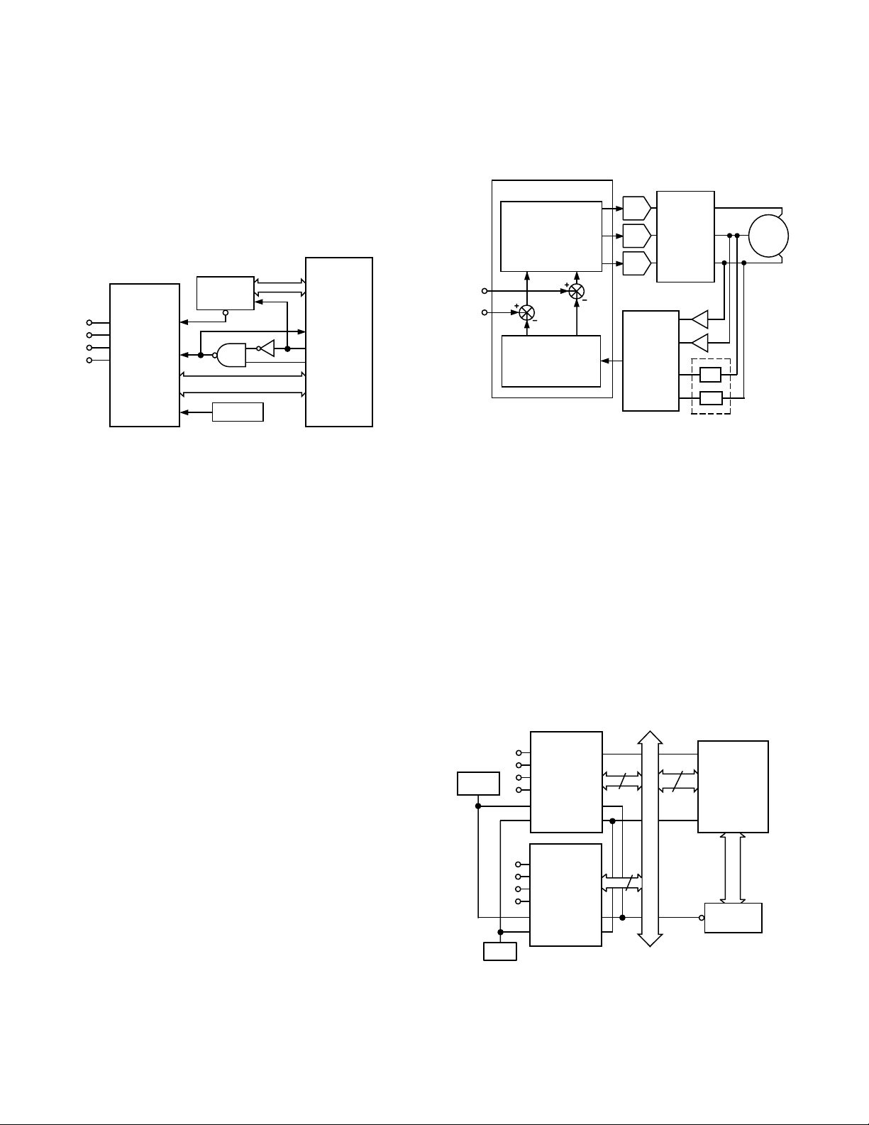
Figure 5 shows the arrangement used. The H/S SEL controls a
multiplexer that selects the source of the conversion sequence
information, i.e., from the hardware channel select pins (SL1 to
SL4) or from the channel selection register. When a conversion
is started the output from the multiplexer is latched until the
end-of-the conversion sequence. The data bus bits DB0 to DB3
(DB0 representing Channel 1 through DB3 representing Channel 4) are bidirectional and become inputs to the channel select
register when RD is logic high and CS and WR are logic low.
The logic state on DB0 to DB3 is latched into the channel select
register when WR goes logic high. Figure 6 shows the loading
sequence for channel selection using software control. When
using software control to select the conversion sequence a write
is only required each time the conversion sequence needs
changing. This is because the channel select register will hold its
information until different information is written to it.
It should be noted that the hardware select Pins SL1 and SL2
are dual function. When H/S SEL is logic high (selecting the
conversion sequence using software control) they take the functions CLK IN and INT/EXT CLK respectively. Therefore, the
logic inputs on these pins must be set according to the type of
operation required (see Using an External Clock). Also when
H/S SEL is high, the SL3 and SL4 logic inputs have no function
and can be tied either high or low, but should not be left floating.
HARDWARE CHANNEL
DATA BUS
CS
WR
SELECT PINS
SL1
SL2
SL3
SL4
D0D1D2D3
CHANNEL
SELECT
REGISTER
WR
TRANSPARENT WHILE WAITING FOR CONVST.
LATCHED ON THE RISING EDGE OF CONVST AND
DURING A CONVERSION SEQUENCE.
H/S
MULTIPLEXER LATCH
SELECT INDIVIDUAL
TRACK-AND-HOLDS
FOR CONVERSION
SEQUENCER
Figure 5. Channel Select Inputs and Registers
–FSR/2 + 5/2 LSB 100 . . . 010 to 100 . . . 011
–FSR/2 + 3/2 LSB 100 . . . 001 to 100 . . . 010
–FSR/2 + 1/2 LSB 100 . . . 000 to 100 . . . 001
NOTES
1
FSR is full-scale range is 5 V, with V
2
1 LSB = FSR/16384 = 610.4 µV (± 2.5 V—AD7865-3) with V
= 2.5 V.
REF
= 2.5 V.
REF
SELECTING A CONVERSION SEQUENCE
Any subset of the four channels V
IN1
to V
can be selected for
IN4
conversion. The selected channels are converted in an ascending
IN1
, V
IN4
IN3
, V
and
IN1
order. For example if the channel selection includes V
and V
then V
then the conversion sequence will be V
IN3
. The conversion sequence selection may be made by
IN4
using either the hardware channel select input pins SL1 through
SL4 (if H/S is tied low) or programming the channel select
register (if H/S is tied high). A logic high on a hardware channel
select pin (or logic one in the channel select register) when
CONVST goes logic high, marks the associated analog input
channel for inclusion in the conversion sequence.
REV. B
–11–
RD
t
13
WR
CS
DATA
t
14
t
16
t
15
DATA IN
t
17
Figure 6. Channel Selection via Software Control

AD7865
TIMING AND CONTROL
Reading Between Each Conversion in the Conversion Sequence
Figure 7 shows the timing and control sequence required to
obtain the optimum throughput rate from the AD7865. To
obtain the optimum throughput from the AD7865 the user must
read the result of each conversion as it becomes available. The
timing diagram in Figure 7 shows a read operation each time the
EOC signal goes logic low. The timing in Figure 7 shows a
conversion on all four analog channels (SL1 to SL4 = 1, see
Selecting a Conversion Sequence), hence there are four EOC
pulses and four read operations to access the result of each of
the four conversions.
A conversion is initiated on the rising edge of CONVST. This
places all four track/holds into hold simultaneously. New data
from this conversion sequence is available for the first channel
selected (A
) 2.4 µs later. The conversion on each subsequent
IN1
channel is completed at 2.4 µs intervals. The end of each con-
version is indicated by the falling edge of the EOC signal. The
BUSY output signal indicates the end of conversion for all
selected channels (four in this case).
Data is read from the part via a 14-bit parallel data bus with
standard CS and RD signals. The CS and RD inputs are internally gated to enable the conversion result onto the data bus.
The data lines DB0 to DB13 leave their high impedance state
when both CS and RD are logic low. Therefore, CS may be
permanently tied logic low and the RD signal used to access the
conversion result. Since each conversion result is latched into its
output data register at the same time EOC goes logic low a
further option would be to tie the EOC and RD pins together
with CS tied logic low and use the rising edge of EOC to latch
the conversion result. Although the AD7865 has some special
features that permit reading during a conversion (e.g., a separate supply for the output data drivers, V
), for optimum
DRIVE
performance it is recommended that the read operation be
completed when EOC is logic low, i.e., before the start of the
next conversion. Although Figure 7 shows the read operation
taking place during the EOC pulse, a read operation can take
place at any time. Figure 7 shows a timing specification called
“Quiet Time.” This is the amount of time that should be left
after a read operation and before the next conversion is initiated. The quiet time heavily depends on data bus capacitance
but a figure of 50 ns to 150 ns is typical.
The signal labeled FRSTDATA (First Data Word) indicates to
the user that the pointer associated with the output data registers is pointing to the first conversion result by going logic high.
The pointer is reset to point to the first data location (i.e., first
conversion result,) at the end of the first conversion just prior to
EOC going low. The pointer is incremented to point to the next
register (next conversion result) by a rising edge of RD only if
that conversion result is available. If a read takes place before
the next conversion is complete (as shown in Figure 7) then the
pointer is incremented at the end of that conversion when the
EOC pulse goes low. Hence, FRSTDATA in Figure 7 is seen to
go low just after to the second EOC pulse. Repeated read
operations during a conversion will continue to access the data
at the current pointer location until the pointer is incremented
at the end of that conversion. Note: FRSTDATA has an indeterminate logic state after initial power-up. This means that for the
first conversion sequence after power-up, the FRSTDATA
logic output may already be logic high before the end of the first
conversion. This condition is indicated by the dashed line in
Figure 7. Also the FRSTDATA logic output may already be
high as a result of the previous read sequence as is the case after
the fourth read in Figure 7. The fourth read (rising edge of RD)
resets the pointer to the first data location. There, however,
FRSTDATA is already high when the next conversion sequence
is initiated.
CONVST
BUSY
EOC
FRSTDATA
RD
CS
DATA
H/S SEL
SL1–SL4
t
1
t
BUSY
t
2
t
CONV
t
100ns
100ns
t
9
t
11
t
12
3
V
t
4
IN1
t
5
t
6
t
7
V
IN2
t
V
CONV
IN3
Figure 7. Timing Diagram for Reading During Conversion
t
ACQ
QUIET
TIME
t
10
V
IN4
–12–
REV. B

AD7865
Accessing the Output Data Registers
There are four Output Data Registers, one for each of the four
possible conversion results from a conversion sequence. The
result of the first conversion in a conversion sequence is placed
in Register 1 and the second result is placed in Register 2 and so
, V
on. For example if the conversion sequence V
IN1
IN3
and V
IN4
is selected (see Selecting a Conversion Sequence) the results of
the conversion on V
IN1
, V
IN3
and V
are placed in Registers 1
IN4
to 3 respectively. The Output Data register pointer is reset to
point to Register 1 at the end of the first conversion in the
sequence, just prior to EOC going low. At this point the logic
output FRSTDATA will go logic high to indicate that the output data register pointer is addressing Register 1. When CS and
RD are both logic low the contents of the addressed register are
enabled onto the data bus (DB0–DB13).
OUTPUT
DATA REGISTERS
(V
2-BIT
COUNTER
POINTER*
RESET
RD
CS
*THE POINTER WILL NOT BE INCREMENTED BY A RISING EDGE ON RD UNTIL
THE CONVERSION RESULT IS IN THE OUTPUT DATA REGISTER. THE POINTER
IS RESET WHEN THE LAST CONVERSION RESULT IS READ
DECODE
OE #1
OE #2
OE #3
OE #4
AD7865
NOT VALID
)
IN1
(V
)
IN3
(V
)
IN4
FRSTDATA
V
DRIVE
O/P
DRIVERS
OE
DB0 TO
DB13
Figure 8. Output Data Registers
When reading the output data registers after a conversion
sequence, i.e., when BUSY goes low, the register pointer is
incremented on the rising edge of the RD signal as shown in
Figure 8. However, when reading the conversion results between
conversions in a conversion sequence the pointer will not be
incremented until a valid conversion result is in the register to
be addressed. In this case the pointer is incremented when the
conversion has ended and the result has been transferred to the
output data register. This happens when EOC goes low, therefore EOC may be used to enable the register contents onto the
data bus as described in Reading Between Conversions in the
Conversion Sequence. The pointer is reset to point to Register 1
on the rising edge of the RD signal when the last conversion
result in the sequence is being read. In the example shown in
Figure 8, this means that the pointer is set to Register 1 when
the contents of Register 3 are read.
Reading after the Conversion Sequence
Figure 9 shows the same conversion sequence as Figure 7. In
this case, however, the results of the four conversions (on V
to V
) are read after all conversions have finished, i.e., when
IN4
IN1
BUSY goes logic low. The FRSTDATA signal goes logic high
at the end of the first conversion just prior to EOC going logic
low. As mentioned previously FRSTDATA has an indeterminate state after initial power up, therefore FRSTDATA may
already be logic high. Unlike the case when reading during a
conversion the output data register pointer is incremented on
the rising edge of RD because the next conversion result is available in this case. This means FRSTDATA will go logic low after
the first rising edge on RD.
Successive read operations will access the remaining conversion
results in ascending channel order. Each read operation increments the output data register pointer. The read operation that
accesses the last conversion result causes the output data register pointer to be reset so that the next read operation will access
the first conversion result again. This is shown in Figure 8 with
the fifth read after BUSY goes low accessing the result of the
conversion on V
. Thus the output data registers acts as a
IN1
circular buffer in which the conversion results may be continually accessed. The FRSTDATA signal will go high when the
first conversion result is available.
Data is enabled onto the data bus DB0 to DB13 using CS and
RD. Both CS and RD have the same functionality as described
in the previous section. There are no restrictions or performance
implications associated with the position of the read operations
after BUSY goes low, however there is a minimum time between
read operations that must be adhered to. Notice also that a “Quiet
Time” is needed before the start of the next conversion sequence.
REV. B
CONVST
BUSY
EOC
DATA
FRSTDATA
t
1
t
BUSY
t
2
t
8
RD
t
CS
3
t
6
V
IN1
t
10
t
V
IN2
t
4
7
V
IN3
V
IN4
Figure 9. Timing Diagram, Reading after the Conversion Sequences
–13–
QUIET
TIME
V
IN1
t
10

AD7865
CLK
CONVST
FRSTDATA
t
18
23456789101112131415161234567891011121314 115 16 1615
EOC
RD
BUSY
FIRST CONVERSION
COMPLETE
Figure 10. Using an External Clock
Using an External Clock
With the H/S SEL and INT/EXT CLK pins tied to Logic 1, the
AD7865 will expect to be driven from an external clock. The
highest external clock frequency allowed is 5 MHz. This means
a conversion time of 3.2 µs compared to 2.4 µs using the inter-
nal clock. In some instances, however, it may be useful to use an
external clock when high throughput rates are not required. For
example, two or more AD7865s may be synchronized by using
the same external clock for all devices. In this way there is no
latency between output logic signals like EOC due to differences
in the frequency of the internal clock oscillators. Figure 10
shows how the various logic outputs are synchronized to the CLK
signal. The first falling edge of CLKIN must not occur until
200 ns after a conversion has been initiated (rising edge of
CONVST), at which point BUSY will go high. The AD7865
will then convert the analog input signal on the first selected
channel (see Selecting a Conversion Sequence) at a rate determined by the CLKIN. No external events will occur until the
14th falling edge of CLKIN. The data register output address
is then reset to point to Data Register 1 and FRSTDATA goes
high. This first conversion is complete on the 15th falling edge
of the CLKIN (indicated by EOC going low) and the result
from this conversion is loaded into Data Register 1. EOC goes
high again on the 16th falling edge of CLKIN. Figure 10 shows
a RD pulse occurring when EOC is low, enabling the conversion
result in Data Register 1 onto the data bus. The next 16 pulses
of CLKIN will convert the analog input signal on the second
selected channel and so on until all selected channels have been
converted. BUSY and EOC will go low on the 15th falling edge
of the last conversion sequence and EOC will return high on the
16th falling edge.
Standby Mode Operation
The AD7865 has a Standby Mode whereby the device can be
placed in a low current consumption mode (3 µA typ). The
AD7865 is placed in standby by bringing the logic input STBY
low. The AD7865 can be powered up again for normal operation by bringing STBY logic high. The output data buffers are
LAST CONVERSION
COMPLETE
still operational while the AD7865 is in standby. This means the
user can still continue to access the conversion results while the
AD7865 is in standby. This feature can be used to reduce the
average power consumption in a system using low throughput
rates. To reduce the average power consumption the AD7865 can
be placed in standby at the end of each conversion sequence,
i.e., when BUSY goes low and taken out of standby again prior
to the start of the next conversion sequence. The time it takes
the AD7865 to come out of standby is called the “wake-up”
time. This wake-up time will limit the maximum throughput
rate at which the AD7865 can be operated when powering down
between conversions. The AD7865 will wake up in less than
1 µs when using an external reference. When the internal reference is used, the wake-up time depends on the amount of time
the AD7865 spends in standby mode. For standby times of less
than 10 ms the AD7865 will wake up in less than 5 µs (see Fig-
ure 11). For standby times greater than this some or all of the
charge on the external reference capacitor will have leaked away
and the wake-up time will be dependent on how long it takes to
recharge. For standby times less than one second the wake-up
time will be less than 1 ms. Even if the charge has been completely
depleted the wake-up time will typically be less than 10 ms.
5
2.5
WAKE-UP TIME – s
0
0
2500
STANDBY TIME – s
5000 7500 10000
Figure 11. Wake-Up Time vs. Standby Time Using the OnChip Reference
–14–
REV. B

CONVST
BUSY
STBY
100s
t
BUSY
7s
t
I
= 3A
DD
WAKEUP
t
BUSY
Figure 12. Power-Down between Conversion Sequences
AD7865
When operating the AD7865 in a standby mode between conversions, the power savings can be significant. For example,
with a throughput rate of 10 kSPS and external reference, the
AD7865 will be powered up 11 µs out of every 100 µs (1 µs for
wake-up time and 9.6 µs to convert four channels. Therefore,
the average power consumption drops to (115 mW × 10.6%) or
12.2 mW approximately.
OFFSET AND FULL-SCALE ADJUSTMENT
In most Digital Signal Processing (DSP) applications, offset and
full-scale errors have little or no effect on system performance.
Offset error can always be eliminated in the analog domain by
ac coupling. Full-scale error effect is linear and does not cause
problems as long as the input signal is within the full dynamic
range of the ADC. Invariably, some applications will require
that the input signal span the full analog input dynamic range.
In such applications, offset and full-scale error will have to be
adjusted to zero.
Figure 13 shows a typical circuit that can be used to adjust the
offset and full-scale errors on the AD7865 (V
on the AD7865-1
1
version is shown for example purposes only). Where adjustment
is required, offset error must be adjusted before full-scale error.
This is achieved by trimming the offset of the op amp driving
the analog input of the AD7865 while the input voltage is
1/2 LSB below analog ground. The trim procedure is as follows:
apply a voltage of –610 µV (–1/2 LSB) at V
and adjust the op
1
amp offset voltage until the ADC output code flickers between
1111 1111 1111 and 0000 0000 0000.
Gain error can be adjusted at either the first code transition
(ADC negative full scale) or the last code transition (ADC positive full scale). The trim procedures for both cases are as follows.
INPUT
RANGE = 10V
V
1
R1
10k
R2
500
R4
10k
R3
10k
*ADDITIONAL PINS OMITTED FOR CLARITY
R5
10k
V
INxA
AD7865*
AGND
Figure 13. Full-Scale Adjust Circuit
Positive Full-Scale Adjust
Apply a voltage of 9.9982 V (FS/2 – 3/2 LSB) at V1. Adjust R2
until the ADC output code flickers between 01 1111 1111 1110
and 01 1111 1111 1111.
Negative Full-Scale Adjust
Apply a voltage of –9.9998 V (–FS + 1/2 LSB) at V1 and adjust
R2 until the ADC output code flickers between 10 0000 0000
0000 and 10 0000 0000 0001.
An alternative scheme for adjusting full-scale error in systems
that use an external reference is to adjust the voltage at the V
REF
pin until the full-scale error for any of the channels is adjusted
out. The good full-scale matching of the channels will ensure
small full-scale errors on the other channels.
DYNAMIC SPECIFICATIONS
The AD7865 is specified and 100% tested for dynamic performance specifications as well as traditional dc specifications such
as Integral and Differential Nonlinearity. These ac specifications
are required for such signal processing applications as phased array
sonar, adaptive filters and spectrum analysis. These applications
require information on the ADC’s effect on the spectral content
of the input signal. Hence, the parameters for which the AD7865
is specified include SNR, harmonic distortion, intermodulation
distortion and peak harmonics. These terms are discussed in
more detail in the following sections.
Signal-to-Noise Ratio (SNR)
SNR is the measured signal-to-noise ratio at the output of the
ADC. The signal is the rms magnitude of the fundamental.
Noise is the rms sum of all the nonfundamental signals up to
half the sampling frequency (f
/2) excluding dc. SNR is depen-
S
dent upon the number of quantization levels used in the digitization
process; the more levels, the smaller the quantization noise. The
theoretical signal to noise ratio for a sine wave input is given by
SNR = (6.02N + 1.76) dB (1)
where N is the number of bits.
Thus for an ideal 14-bit converter, SNR = 86.04 dB.
Figure 14 shows a histogram plot for 8192 conversions of a dc
input using the AD7865 with 5 V supply. The analog input was
set at the center of a code transition. It can be seen that most of
the codes appear in the one output bin, indicating very good
noise performance from the ADC.
REV. B
–15–

AD7865
7000
6000
5000
4000
3000
COUNTS
2000
1000
0
ADC CODE
Figure 14. Histogram of 8192 Conversions of a DC Input
The output spectrum from the ADC is evaluated by applying a
sine wave signal of very low distortion to the analog input. A
Fast Fourier Transform (FFT) plot is generated from which the
SNR data can be obtained. Figure 15 shows a typical 4096point FFT plot of the AD7865 with an input signal of 100 kHz
and a sampling frequency of 350 kHz. The SNR obtained from
this graph is 80.5 dB. It should be noted that the harmonics are
taken into account when calculating the SNR.
0
–20
fs = 350kHz
–40
–60
dBs
–80
–100
–120
fIN = 100kHz
SNR = 80.5dB
14
13
12
11
10
9
8
7
ENOB
6
5
4
3
2
1
0
0
100
INPUT FREQUENCY – kHz
1000 10000
–55C
+25C
+125C
Figure 16. Effective Numbers of Bits vs. Frequency
Intermodulation Distortion
With inputs consisting of sine waves at two frequencies, fa and
fb, any active device with nonlinearities will create distortion
products at sum and difference frequencies of mfa ± nfb where
m, n = 0, 1, 2, 3 . . ., etc. Intermodulation terms are those for
which neither m nor n are equal to zero. For example, the second order terms include (fa + fb) and (fa – fb) while the third
order terms include (2fa + fb), (2fa – fb), (fa + 2fb) and (fa – 2fb).
The AD7865 is tested using two input frequencies. In this case
the second and third order terms are of different significance.
The second order terms are usually distanced in frequency from
the original sine waves while the third order terms are usually at
a frequency close to the input frequencies. As a result, the second
and third order terms are specified separately. The calculation of
the intermodulation distortion is as per the THD specification
where it is the ratio of the rms sum of the individual distortion
products to the rms amplitude of the fundamental expressed in
dBs. In this case, the input consists of two, equal amplitude, low
distortion sine waves. Figure 17 shows a typical IMD plot for
the AD7865.
–140
0 35000 70000
FREQUENCY – Hz
105000 140000 175000
Figure 15. FFT Plot
Effective Number of Bits
The formula given in Equation 1 relates the SNR to the number
of bits. Rewriting the formula, as in Equation 2, it is possible to
obtain a measure of performance expressed in effective number
of bits (N).
SNR=−176
N
602..
(2)
The effective number of bits for a device can be calculated
directly from its measured SNR. Figure 16 shows a typical plot
of effective number of bits versus frequency for an AD7865-2.
–16–
dBs
–100
–120
–140
–20
–40
–60
–80
0
0
25000 50000
FREQUENCY – Hz
Figure 17. IMD Plot
fa = 49.113kHz
f
b = 50.183kHz
f
= 350kHz
s
75000
100000 125000 175000
150000
REV. B

AD7865
AC Linearity Plots
The plots shown in Figure 18 below show typical DNL and INL
for the AD7865.
0.60
0
DNL – LSBs
–0.60
0 4000 8000 12000 16383
0.60
0
iNL – LSBs
–0.60
0 4000 8000 12000 16383
ADC – Code
ADC – Code
Figure 18. Typical DNL and INL Plots
MICROPROCESSOR INTERFACING
The high speed parallel interface of the AD7865 allows easy
interfacing to most DSPs and microprocessors. The AD7865
interface of the AD7865 consists of the data lines (DB0 to
DB13), CS, RD, WR, EOC and BUSY.
AD7865–ADSP-21xx Interface
Figure 19 shows an interface between the AD7865 and the
ADSP-210x. The CONVST signal can be generated by the
ADSP-210x or from some other external source. Figure 19
shows the CS being generated by a combination of the DMS
signal and the address bus of the ADSP-2100. In this way the
AD7865 is mapped into the data memory space of the
ADSP-210x.
The AD7865 BUSY line provides an interrupt to the ADSP210x when the conversion sequence is complete on all the
selected channels. The conversion results can then be read from
the AD7865 using successive read operations. Alternately, one
can use the EOC pulse to interrupt the ADSP-210x when the
conversion on each channel is complete when reading between
each conversion in the conversion sequence (Figure 8). The
AD7865 is read using the following instruction
MR0 = DM(ADC)
where MR0 is the ADSP-210x MR0 register and ADC is the
AD7865 address.
ADSP-21xx
A0–A13
DMS
RD
WR
D0–D13
IRQn
DT1/F0
V
IN1
V
IN2
V
IN3
V
IN4
AD7865
WR
DB0–DB13
BUSY
CONVST
CS
RD
ADDRESS
DECODE
Figure 19. AD7865–ADSP-21xx Interface
AD7865–TMS320C5x Interface
Figure 20 shows an interface between the AD7865 and the
TMS320C5x. As with the previous interfaces, conversion can be
initiated from the TMS320C5x or from an external source and
the processor is interrupted when the conversion sequence is
completed. The CS signal to the AD7865 derived from the DS
signal and a decode of the address bus. This maps the AD7865
into external data memory. The RD signal from the TMS320 is
used to enable the ADC data onto the data bus. The AD7865
has a fast parallel bus so there are no wait state requirements.
The following instruction is used to read the conversion results
from the AD7865:
IN D,ADC
where D is Data Memory address and ADC is the AD7865
address.
TMS320C5x
A0–A13
DS
RD
WR
D0–D13
INTn
PA0
V
IN1
V
IN2
V
IN3
V
IN4
AD7865
WR
DB0–DB13
BUSY
CONVST
CS
RD
ADDRESS
DECODE
Figure 20. AD7865–TMS320C5x Interface
AD7865–MC68000 Interface
An interface between the AD7865 and the MC68000 is shown
in Figure 21. The conversion can be initiated from the MC68000
or from an external source. The AD7865 BUSY line can be
used to interrupt the processor or, alternatively, software delays
can ensure that conversion has been completed before a read to
the AD7865 is attempted. Because of the nature of its interrupts, the 68000 requires additional logic (not shown in Figure
21) to allow it to be interrupted correctly. For further information on 68000 interrupts, consult the 68000 users manual.
REV. B
–17–
AD7865
The MC68000 AS and R/W outputs are used to generate a
separate RD input signal for the AD7865. CS is used to drive
the 68000 DTACK input to allow the processor to execute a
normal read operation to the AD7865. The conversion results
are read using the following 68000 instruction:
MOVE.W ADC,D0
where D0 is the 68000 D0 register and ADC is the AD7865
address.
MC68000
A0–A15
DTACK
AS
R/W
D0–D13
V
IN1
V
IN2
V
IN3
V
IN4
AD7865
DB0–DB13
CONVST
RD
CS
ADDRESS
DECODE
CLOCK
Figure 21. AD7865–MC68000 Interface
Vector Motor Control
The current drawn by a motor can be split into two components: one produces torque and the other produces magnetic
flux. For optimal performance of the motor, these two components should be controlled independently. In conventional
methods of controlling a three-phase motor, the current (or
voltage) supplied to the motor and the frequency of the drive are
the basic control variables. However, both the torque and flux
are functions of current (or voltage) and frequency. This coupling effect can reduce the performance of the motor because,
for example, if the torque is increased by increasing the frequency, the flux tends to decrease.
Vector control of an ac motor involves controlling phase in
addition to drive and current frequency. Controlling the phase
of the motor requires feedback information on the position of
the rotor relative to the rotating magnetic field in the motor.
Using this information, a vector controller mathematically transforms the three phase drive currents into separate torque and
flux components. The AD7865, with its four-channel simultaneous sampling capability, is ideally suited for use in vector
motor control applications.
A block diagram of a vector motor control application using the
AD7865 is shown in Figure 22. The position of the field is
derived by determining the current in each phase of the motor.
Only two phase currents need to be measured because the third
can be calculated if two phases are known. V
IN1
and V
IN2
of the
AD7865 are used to digitize this information.
Simultaneous sampling is critical to maintain the relative phase
information between the two channels. A current sensing isolation amplifier, transformer or Hall-effect sensor is used between
the motor and the AD7865. Rotor information is obtained by
measuring the voltage from two of the inputs to the motor. V
and V
of the AD7865 are used to obtain this information.
IN4
IN3
Once again, the relative phase of the two channels is important.
A DSP microprocessor is used to perform the mathematical
transformations and control loop calculations on the information fed back by the AD7865.
DSP MICROPROCESSOR
TORQUE AND FLUX
CONTROL LOOP
CALCULATIONS AND
TWO-TO -THREE-
PHASE INFORMATION
TORQUE
SETPOINT
FLUX
SETPOINT
TRANSFORMATION
TO TORQUE AND
FLUX CURRENT
COMPONENTS
*ADDITIONAL PINS OMITTED FOR CLARITY
DAC
DAC
DAC
AD7865*
DRIVE
CIRCUITRY
ISOLATION
AMPLIFIERS
V
IN1
V
IN2
V
IN3
V
IN4
I
C
I
B
I
A
VOLTAGE
ATTENUATORS
V
B
V
A
3-
PHASE
MOTOR
Figure 22. Vector Motor Control Using the AD7865
MULTIPLE AD7865s IN A SYSTEM
Figure 23 shows a system where a number of AD7865s can be
configured to handle multiple input channels. This type of configuration is common in applications such as sonar, radar, etc.
The AD7865 is specified with maximum limits on aperture
delay match. This means that the user knows the difference in
the sampling instant between all channels. This allows the user
to maintain relative phase information between the different
channels. The AD7865 has a maximum aperture delay matching of ±4 ns.
All AD7865s use the same external SAR clock (5 MHz). Therefore, the conversion time for all devices will be the same and so
all devices may be read simultaneously. In the example shown in
Figure 23, the data outputs of two AD7865s are enabled onto a
32-bit wide data bus when EOC goes low.
AD7865
AD780
V
V
V
V
V
CLK IN
V
V
V
V
V
CLK IN
5MHz
IN1
IN2
IN3
IN4
REF
AD7865
IN1
IN2
IN3
IN4
REF
EOC
CS
RD
CS
RD
ADSP-2106x
14
14
32
RD
ADDRESS
DECODE
Figure 23. Multiple AD7865s in Multichannel System
–18–
REV. B

0.037 (0.94)
0.025 (0.64)
SEATING
PLANE
OUTLINE DIMENSIONS
Dimensions shown in inches and (mm).
44-Lead Plastic Quad Flatpack
(S-44)
0.548 (13.925)
0.096 (2.44)
MAX
8
0.8
34
0.546 (13.875)
0.398 (10.11)
0.390 (9.91)
33
AD7865
23
22
0.040 (1.02)
0.032 (0.81)
0.083 (2.11)
0.077 (1.96)
0.040 (1.02)
0.032 (0.81)
44
1
0.033 (0.84)
0.029 (0.74)
TOP VIEW
(PINS DOWN)
C01342a–0–12/00 (rev. B)
12
11
0.016 (0.41)
0.012 (0.30)
REV. B
PRINTED IN U.S.A.
–19–
 Loading...