

Single- and 4-Channel, 9 s, 10-Bit ADCs
with On-Chip Temperature Sensor
AD7816/AD7817/AD7818
FEATURES
10-Bit ADC with 9 s Conversion Time
One (AD7818) and Four (AD7817) Single-Ended Analog
Input Channels
The AD7816 Is a Temperature Measurement Only Device
On-Chip Temperature Sensor
Resolution of 0.25ⴗC
ⴞ2ⴗC Error from –40ⴗC to +85ⴗC
–55ⴗC to +125ⴗC Operating Range
Wide Operating Supply Range
2.7 V to 5.5 V
Inherent Track-and-Hold Functionality
On-Chip Reference (2.5 V ⴞ 1%)
Overtemperature Indicator
Automatic Power-Down at the End of a Conversion
Low Power Operation
4 W at a Throughput Rate of 10 SPS
40 W at a Throughput Rate of 1 kSPS
400 W at a Throughput Rate of 10 kSPS
Flexible Serial Interface
APPLICATIONS
Ambient Temperature Monitoring (AD7816)
Thermostat and Fan Control
High Speed Microprocessor
Temperature Measurement and Control
Data Acquisition Systems with Ambient Temperature
Monitoring (AD7817 and AD7818)
Industrial Process Control
Automotive
Battery Charging Applications
GENERAL DESCRIPTION
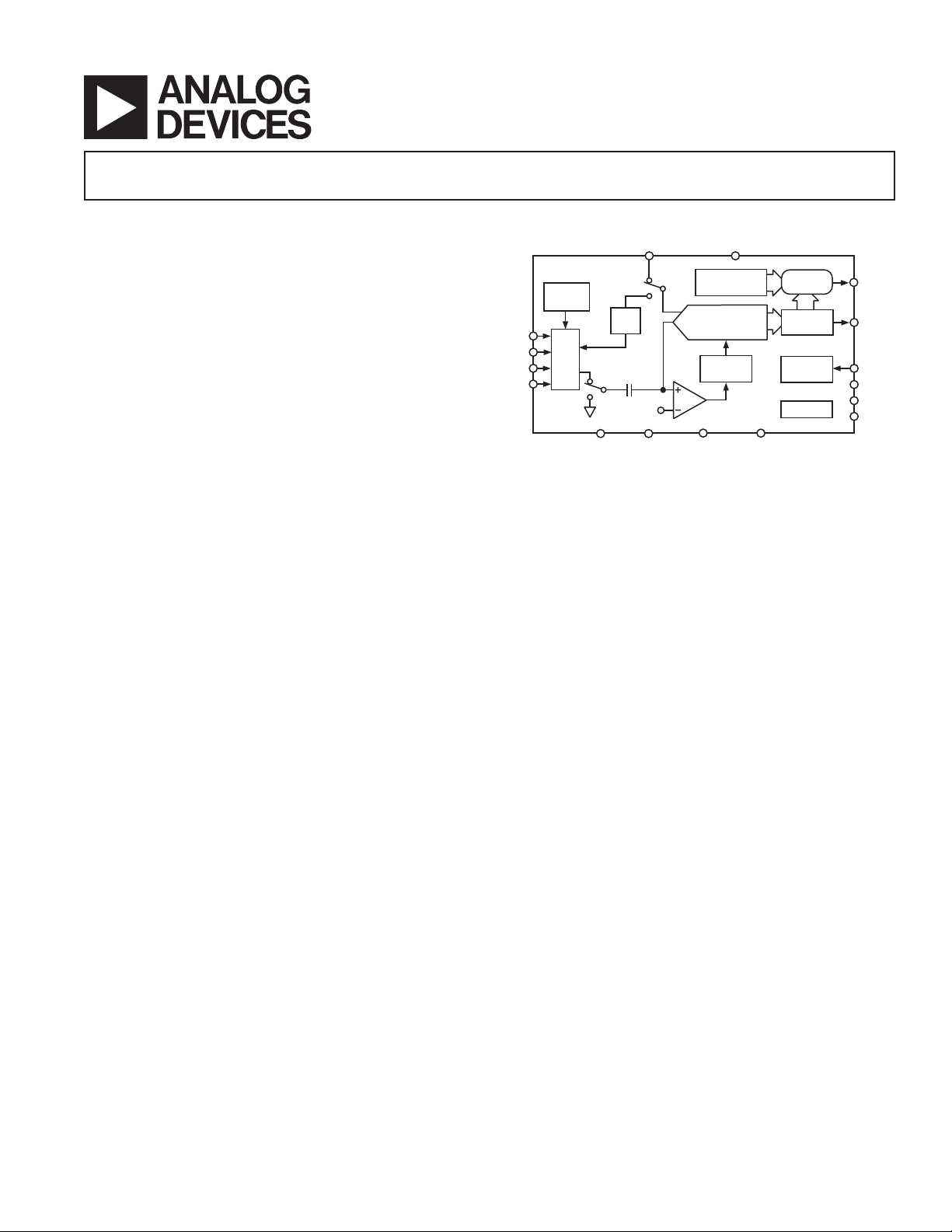
The AD7818 and AD7817 are 10-bit, single- and 4-channel
A/D converters with on-chip temperature sensor that can operate from a single 2.7 V to 5.5 V power supply. Each part contains a 9 µs successive-approximation converter based around
a capacitor DAC, an on-chip temperature sensor with an accuracy of ⫾2°C, an on-chip clock oscillator, inherent track-andhold functionality and an on-chip reference (2.5 V). The
AD7816 is a temperature monitoring only device in a SOIC/
MSOP package.
The on-chip temperature sensor of the AD7817 and AD7818
can be accessed via Channel 0. When Channel 0 is selected and
a conversion is initiated, the resulting ADC code at the end of
the conversion gives a measurement of the ambient temperature
with a resolution of ⫾0.25°C. See Temperature Measurement
section of this data sheet.
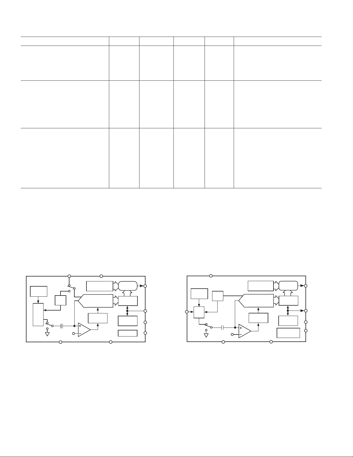
FUNCTIONAL BLOCK DIAGRAM
REF
IN
AD7817
TEMP
SENSOR
V
IN1
V
IN2
V
V
MUX
IN3
IN4
SAMPLING
CAPACITOR
V
AGND
REF
2.5V
BALANCE
DGND
V
DD
OVERTEMP
REG
CHARGE
REDISTRIBUTION
DAC
CONTROL
LOGIC
BUSY
CONVST
B
CONTROL
A > B
A
DATA
OUT
REG
CLOCK
OTI
D
OUT
D
IN
SCLK
RD/WR
CS
The AD7816, AD7817, and AD7818 have a flexible serial
interface that allows easy interfacing to most microcontrollers.
The interface is compatible with the Intel 8051, Motorola
®
and QSPI™ protocols and National Semiconductors
SPI
MICROWIRE™ protocol. For more information refer to the
Serial Interface section of this data sheet.
The AD7817 is available in a narrow body 0.15" 16-lead small
outline IC (SOIC), in a 16-lead, thin shrink small outline package (TSSOP), while the AD7816/AD7818 come in an 8-lead
small outline IC (SOIC) and an 8-lead microsmall outline IC
(MSOP).
PRODUCT HIGHLIGHTS
1. The devices have an on-chip temperature sensor that allows an
accurate measurement of the ambient temperature to be
made. The measurable temperature range is –55°C to +125°C.
2. An overtemperature indicator is implemented by carrying out a
digital comparison of the ADC code for Channel 0 (temperature sensor) with the contents of the on-chip overtemperature
register. The overtemperature indicator pin goes logic low when
a predetermined temperature is exceeded.
3. The automatic power-down feature enables the AD7816,
AD7817, and AD7818 to achieve superior power performance at slower throughput rates, e.g., 40 µW at 1 kSPS
throughput rate.
REV. C
Information furnished by Analog Devices is believed to be accurate and
reliable. However, no responsibility is assumed by Analog Devices for its
use, nor for any infringements of patents or other rights of third parties that
may result from its use. No license is granted by implication or otherwise
under any patent or patent rights of Analog Devices. Trademarks and
registered trademarks are the property of their respective owners.
One Technology Way, P.O. Box 9106, Norwood, MA 02062-9106, U.S.A.
Tel: 781/329-4700 www.analog.com
Fax: 781/326-8703 © 2004 Analog Devices, Inc. All rights reserved.

AD7816/AD7817/AD7818
AD7817–SPECIFICATIONS
Parameter A Version *B Version *S Version Unit Test Conditions/Comments
DYNAMIC PERFORMANCE Sample Rate = 100 kSPS, Any
2
Signal to (Noise + Distortion) Ratio
Total Harmonic Distortion
Peak Harmonic or Spurious Noise2–65 –65 –65 dB max –75 dB typ
Intermodulation Distortion
2
2
Second Order Terms –67 –67 –67 dB typ
Third Order Terms –67 –67 –67 dB typ
Channel-to-Channel Isolation
2
DC ACCURACY Any Channel
Resolution 10 10 10 Bits
Minimum Resolution for Which
No Missing Codes are Guaranteed 10 10 10 Bits
Relative Accuracy
Differential Nonlinearity
Gain Error
Gain Error Match
Offset Error
2
2
2
2
2
Offset Error Match ⫾1/2 ⫾1/2 ⫾ 1/2 LSB max
TEMPERATURE SENSOR
1
Measurement Error External Reference V
Ambient Temperature 25°C ⫾2 ⫾1 ⫾2 °C max
to T
T
MIN
MAX
Measurement Error On-Chip Reference
Ambient Temperature 25°C ⫾2.25 ⫾2.25 ⫾2.25 °C max
to T
T
MIN
MAX
Temperature Resolution 1/4 1/4 1/4 °C/LSB
REFERENCE INPUT
REFIN Input Voltage Range
3, 4
3
Input Impedance 40 40 40 kΩ min
Input Capacitance 10 10 10 pF max
ON-CHIP REFERENCE
Temperature Coefficient
CONVERSION RATE
Track/Hold Acquisition Time
5
3
4
Conversion Time
Temperature Sensor 27 27 27 µs max
Channels 1 to 4 9 9 9 µs max
POWER REQUIREMENTS
V
DD
I
DD
Normal Operation 2 2 2 mA max 1.6 mA typ
Using External Reference 1.75 1.75 1.75 mA max 2.5 V External Reference Connected
Power-Down (V
Power-Down (V
= 5 V) 10 10 12.5 µA max 5.5 µA typ
DD
= 3 V) 4 4 4.5 µA max 2 µA typ
DD
Auto Power-Down Mode V
10 SPS Throughput Rate 6.4 6.4 6.4 µW typ See Power vs. Throughput Section for
1 kSPS Throughput Rate 48.8 48.8 48.8 µW typ Description of Power Dissipation in
10 kSPS Throughput Rate 434 434 434 µW typ Auto Power-Down Mode
Power-Down 12 12 13.5 µW max Typically 6 µW
58 58 58 dB min
–65 –65 –65 dB max –75 dB typ
–80 –80 –80 dB typ fIN = 20 kHz
⫾1 ⫾1 ⫾1LSB max
⫾1 ⫾1 ⫾1LSB max
⫾2 ⫾2 ⫾2LSB max External Reference
⫾10 ⫾10 +20/–10 LSB max Internal Reference
⫾1/2 ⫾1/2 ⫾ 1/2 LSB max
⫾2 ⫾2 ⫾2LSB max
⫾3 ⫾2 ⫾3 °C max
⫾3 ⫾3 ⫾6 °C max
2.625 2.625 2.625 V max 2.5 V + 5%
2.375 2.375 2.375 V min 2.5 V – 5%
80 80 150 ppm/°C typ
400 400 400 ns max Source Impedance < 10 Ω
5.5 5.5 5.5 V max For Specified Performance
2.7 2.7 2.7 V min
(VDD = 2.7 V to 5.5 V, GND = 0 V, REFIN = 2.5 V unless otherwise noted)
Channel, fIN = 20 kHz
fa =19.9 kHz, fb = 20.1 kHz
Nominal 2.5 V
Logic Inputs = 0 V or V
= 3 V
DD
= 2.5 V
REF
DD
1
REV. C–2–

AD7816/AD7817/AD7818
1
AD7816/AD78186–SPECIFICATIONS
Parameter A Version Unit Test Conditions/Comments
DYNAMIC PERFORMANCE (AD7818 Only) Sample Rate = 100 kSPS, Any Channel,
Signal to (Noise + Distortion) Ratio
Total Harmonic Distortion
Peak Harmonic or Spurious Noise
Intermodulation Distortion
2
2
Second Order Terms –67 dB typ
Third Order Terms –67 dB typ
Channel-to-Channel Isolation
DC ACCURACY (AD7818 Only) Any Channel
Resolution 10 Bits
Minimum Resolution for Which
No Missing Codes are Guaranteed 10 Bits
Relative Accuracy
Differential Nonlinearity
Gain Error
Offset Error
TEMPERATURE SENSOR
2
2
2
2
1
Measurement Error External Reference V
Ambient Temperature 25°C ⫾2 °C max
to T
T
MIN
MAX
Measurement Error On-Chip Reference
Ambient Temperature 25°C ⫾2 °C max
to T
T
MIN
MAX
Temperature Resolution 1/4 °C/LSB
REFERENCE INPUT
Input Voltage Range
REF
IN
3, 4
(AD7816 Only)
3
Input Impedance 50 kΩ min
Input Capacitance 10 pF max
ON-CHIP REFERENCE
Temperature Coefficient
5
3
CONVERSION RATE
Track/Hold Acquisition Time
Conversion Time
Temperature Sensor 27 µs max
Channel 1 9 µs max (AD7818 Only)
POWER REQUIREMENTS
V
DD
I
DD
Normal Operation 2 mA max 1.3 mA typ
Using External Reference 1.75 mA max 2.5 V External Reference Connected
Power-Down (V
Power-Down (V
= 5 V) 10.75 µA max 6 µA typ
DD
= 3 V) 4.5 µA max 2 µA typ
DD
Auto Power-Down Mode V
10 SPS Throughput Rate 6.4 µW typ See Power vs. Throughput Section for
1 kSPS Throughput Rate 48.8 µW typ Description of Power Dissipation in
10 kSPS Throughput Rate 434 µW typ Auto Power-Down Mode
Power-Down 13.5 µW max Typically 6 µW
2
2
2
57 dB min
–65 dB max –75 dB typ
–67 dB typ –75 dB typ
–80 dB typ fIN = 20 kHz
⫾1 LSB max
⫾1 LSB max
⫾10 LSB max
⫾4 LSB max
⫾3 °C max
⫾3 °C max
2.625 V max 2.5 V + 5%
2.375 V min 2.5 V – 5%
30 ppm/°C typ
4
400 ns max Source Impedance < 10 Ω
5.5 V max For Specified Performance
2.7 V min
(VDD = 2.7 V to 5.5 V, GND = 0 V, REFIN = 2.5 V unless
otherwise noted)
fIN = 20 kHz
fa = 19.9 kHz, fb = 20.1 kHz
= 2.5 V
REF
Nominal 2.5 V
Logic Inputs = 0 V or V
= 3 V
DD
DD
REV. C
–3–
AD7816/AD7817/AD7818–SPECIFICATIONS
Parameter A Version *B Version *S Version Unit Test Conditions/Comments
ANALOG INPUTS
Input Voltage Range V
Input Leakage ⫾1 ⫾1 ⫾ 1 µA min
Input Capacitance 10 10 10 pF max
LOGIC INPUTS
Input High Voltage, V
Input Low Voltage, V
Input High Voltage, V
Input Low Voltage, V
Input Current, I
Input Capacitance, C
LOGIC OUTPUTS
Output High Voltage, V
Output Low Voltage, V
High Impedance Leakage Current ⫾1 ⫾1 ⫾ 1 µA max
High Impedance Capacitance 15 15 15 pF max
NOTES
*B and S Versions apply to AD7817 only. For operating temperature ranges, see Ordering Guide.
1
AD7816 and AD7817 temperature sensors specified with external 2.5 V reference, AD7818 specified with on-chip reference. All other specifications with external
and on-chip reference (2.5 V). For VDD = 2.7 V, TA = 85°C max and temperature sensor measurement error = ⫾3°C.
2
See Terminology.
3
The accuracy of the temperature sensor is affected by reference tolerance. The relationship between the two is explained in the section titled Temperature Measurement Error Due to Reference Error.
4
Sample tested during initial release and after any redesign or process change that may affect this parameter.
5
On-chip reference shuts down when external reference is applied.
6
All specifications are typical for AD7818 at temperatures above 85°C and with VDD greater than 3.6 V.
7
Refers to the input current when the part is not converting. Primarily due to reverse leakage current in the ESD protection diodes.
Specifications subject to change without notice.
7
REF
V
REF
V
REF
V max
(AD7817 and AD7818)
0 00V min
4
INH
INL
INH
INL
IN
IN
4
OH
OL
2.4 2.4 2.4 V min VDD = 5 V ⫾ 10%
0.8 0.8 0.8 V max VDD = 5 V ⫾ 10%
2 22V minV
= 3 V ⫾ 10%
DD
0.4 0.4 0.4 V max VDD = 3 V ⫾ 10%
⫾3 ⫾3 ⫾ 3 µA max Typically 10 nA, VIN = 0 V to V
10 10 10 pF max
I
= 200 µA
4 44V minV
2.4 2.4 2.4 V min V
0.4 0.4 0.4 V max V
0.2 0.2 0.2 V max V
SOURCE
= 5 V ⫾ 10%
DD
= 3 V ⫾ 10%
DD
I
= 200 µA
SINK
= 5 V ⫾ 10%
DD
= 3 V ⫾ 10%
DD
DD
V
DD
OVERTEMP
REG
CHARGE
REDISTRIBUTION
DAC
CONTROL
LOGIC
CONVST
B
CONTROL
A > B
A
DATA
OUT
REG
CLOCK
AD7816
TEMP
SENSOR
MUX
REF
REF
2.5V
SAMPLING
CAPACITOR
V
BALANCE
AGND
IN
Figure 1. AD7816 Functional Block Diagram
OTI
D
OUT
IN/
SCLK
RD/WR
V
DD
AD7818
TEMP
SENSOR
V
MUX
IN1
REF
2.5V
SAMPLING
CAPACITOR
V
BALANCE
AGND
OVERTEMP
REG
CHARGE
REDISTRIBUTION
DAC
CONTROL
LOGIC
CONVST
Figure 2. AD7818 Functional Block Diagram
A > B
B
A
DATA
OUT
CONTROL
REG
CLOCK
GENERATOR
OTI
D
OUT
IN/
SCLK
RD/WR
REV. C–4–
AD7816/AD7817/AD7818
TIMING CHARACTERISTICS
(VDD = 2.7 V to 5.5 V, GND = 0 V, REFIN = 2.5 V. All specifications T
1, 2
otherwise noted)
MIN
to T
MAX
unless
Parameter A, B Versions Unit Test Conditions/Comments
t
POWER-UP
t
1a
t
1b
t
2
t
3
t
4
t
5
t
6
t
7
t
8
t
9
t
10
t
11
3
t
12
3
t
13
3, 4
t
14a
3, 4
t
14b
t
15
t
16
t
17
NOTES
1
Sample tested during initial release and after any redesign or process change that may affect this parameter. All input signals are measured with tr = tf = 1 ns (10% to
90% of 5 V) and timed from a voltage level of 1.6 V.
2
See Figures 16, 17, 20 and 21.
3
These figures are measured with the load circuit of Figure 3. They are defined as the time required for D
or 2 V for VDD = 3 V ⫾ 10%, as quoted on the specifications page of this data sheet.
4
These times are derived from the measured time taken by the data outputs to change 0.5 V when loaded with the circuit of Figure 3. The measured number is then
extrapolated back to remove the effects of charging or discharging the 50 pF capacitor. This means that the times quoted in the timing characteristics are the true bus
relinquish times of the part and as such are independent of external bus loading capacitances.
Specifications subject to change without notice.
2 µs max Power-Up Time from Rising Edge of CONVST
9 µs max Conversion Time Channels 1 to 4
27 µs max Conversion Time Temperature Sensor
20 ns min CONVST Pulse Width
50 ns max CONVST Falling Edge to BUSY Rising Edge
0 ns min CS Falling Edge to RD/WR Falling Edge Setup Time
0 ns min RD/WR Falling Edge to SCLK Falling Edge Setup
10 ns min DIN Setup Time before SCLK Rising Edge
10 ns min DIN Hold Time after SCLK Rising Edge
40 ns min SCLK Low Pulse Width
40 ns min SCLK High Pulse Width
0 ns min CS Falling Edge to RD/WR Rising Edge Setup Time
0 ns min RD/WR Rising Edge to SCLK Falling Edge Setup Time
20 ns max D
20 ns max D
30 ns max D
30 ns max D
Access Time after RD/WR Rising Edge
OUT
Access Time after SCLK Falling Edge
OUT
Bus Relinquish Time after Falling Edge of RD/WR
OUT
Bus Relinquish Time after Rising Edge of CS
OUT
150 ns max BUSY Falling Edge to OTI Falling Edge
40 ns min RD/WR Rising Edge to OTI Rising Edge
400 ns min SCLK Rising Edge to CONVST Falling Edge (Acquisition Time of T/H)
to cross 0.8 V or 2.4 V for VDD = 5 V ⫾ 10% and 0.4 V
OUT
I
OL
1.6V
I
OL
TO
OUTPUT
PIN
50pF
200A
C
L
200A
Figure 3. Load Circuit for Access Time and Bus Relinquish Time
REV. C
–5–
AD7816/AD7817/AD7818
ABSOLUTE MAXIMUM RATINGS
(
TA = 25°C unless otherwise noted)
1
VDD to AGND . . . . . . . . . . . . . . . . . . . . . . . . . –0.3 V to +7 V
to DGND . . . . . . . . . . . . . . . . . . . . . . . . . –0.3 V to +7 V
V
DD
Analog Input Voltage to AGND
to V
V
IN1
Reference Input Voltage to AGND
Digital Input Voltage to DGND . . . . . . –0.3 V to V
Digital Output Voltage to DGND . . . . . –0.3 V to V
. . . . . . . . . . . . . . . . . . . –0.3 V to VDD + 0.3 V
IN4
2
. . . –0.3 V to V
DD
DD
DD
+ 0.3 V
+ 0.3 V
+ 0.3 V
Storage Temperature Range . . . . . . . . . . . . . –65°C to +150°C
Junction Temperature . . . . . . . . . . . . . . . . . . . . . . . . . . 150°C
TSSOP, Power Dissipation . . . . . . . . . . . . . . . . . . . . 450 mW
Thermal Impedance . . . . . . . . . . . . . . . . . . . . . 120°C/W
θ
JA
Lead Temperature, Soldering . . . . . . . . . . . . . . . . . . 260°C
Vapor Phase (60 sec) . . . . . . . . . . . . . . . . . . . . . . . 215°C
Infrared (15 sec) . . . . . . . . . . . . . . . . . . . . . . . . . . 220°C
16-Lead SOIC Package, Power Dissipation . . . . . . . . 450 mW
Thermal Impedance . . . . . . . . . . . . . . . . . . . . . 100°C/W
θ
JA
Lead Temperature, Soldering
Vapor Phase (60 sec) . . . . . . . . . . . . . . . . . . . . . . . 215°C
Infrared (15 sec) . . . . . . . . . . . . . . . . . . . . . . . . . . 220°C
8-Lead SOIC Package, Power Dissipation . . . . . . . . . . 450 mW
Thermal Impedance . . . . . . . . . . . . . . . . . . . . . 157°C/W
θ
JA
Lead Temperature, Soldering
Vapor Phase (60 sec) . . . . . . . . . . . . . . . . . . . . . . . 215°C
Infrared (15 sec) . . . . . . . . . . . . . . . . . . . . . . . . . . 220°C
µSOIC Package, Power Dissipation . . . . . . . . . . . . . . 450 mW
θ
Thermal Impedance . . . . . . . . . . . . . . . . . . . . . 206°C/W
JA
Lead Temperature, Soldering
Vapor Phase (60 sec) . . . . . . . . . . . . . . . . . . . . . . . 215°C
Infrared (15 sec) . . . . . . . . . . . . . . . . . . . . . . . . . . 220°C
NOTES
1
Stresses above those listed under Absolute Maximum Ratings may cause permanent damage to the device. This is a stress rating only; functional operation of the
device at these or any other conditions above those listed in the operational sections
of this specification is not implied. Exposure to absolute maximum rating conditions for extended periods may affect device reliability.
2
If the Reference Input Voltage is likely to exceed VDD by more than 0.3 V (e.g.,
during power-up) and the reference is capable of supplying 30 mA or more, it is
recommended to use a clamping diode between the REFIN pin and VDD pin. The
diagram below shows how the diode should be connected.
BAT81
V
DD
REF
IN
AD7816/AD7817
REV. C–6–

AD7816/AD7817/AD7818
ORDERING GUIDE
Temperature Temperature Package Package
Model Range Error @ +25°C Description Options Branding
AD7816AR –40°C to +85°C ± 2°C 8-Lead Narrow Body (SOIC) R-8
AD7816AR-REEL –40°C to +85°C ± 2°C 8-Lead Narrow Body (SOIC) R-8
AD7816AR-REEL7 –40°C to +85°C ±2°C 8-Lead Narrow Body (SOIC) R-8
AD7816ARM –40°C to +85°C ±2°C 8-Lead MSOP RM-8 C4A
AD7816ARM-REEL –40°C to +85°C ±2°C 8-Lead MSOP RM-8 C4A
AD7816ARM-REEL7 –40°C to +85°C ± 2°C 8-Lead MSOP RM-8 C4A
AD7816ACHIPS Die
AD7817AR –40°C to +85°C ± 2°C 16-Lead Narrow Body (SOIC) R-16
AD7817AR-REEL –40°C to +85°C ± 2°C 16-Lead Narrow Body (SOIC) R-16
AD7817AR-REEL7 –40°C to +85°C ± 2°C 16-Lead Narrow Body (SOIC) R-16
AD7817ARZ* –40°C to +85°C ±2°C 16-Lead Narrow Body (SOIC) R-16
AD7817ARU –40°C to +85°C ± 2°C 16-Lead (TSSOP) RU-16
AD7817ARU-REEL –40°C to +85°C ± 2°C 16-Lead (TSSOP) RU-16
AD7817ARU-REEL7 –40°C to +85°C ± 2°C 16-Lead (TSSOP) RU-16
AD7817BR –40°C to +85°C ± 1°C 16-Lead Narrow Body (SOIC) R-16
AD7817BR-REEL –40°C to +85°C ± 1°C 16-Lead Narrow Body (SOIC) R-16
AD7817BR-REEL7 –40°C to +85°C ± 1°C 16-Lead Narrow Body (SOIC) R-16
AD7817BRZ* –40°C to +85°C ± 1°C 16-Lead Narrow Body (SOIC) R-16
AD7817BRZ-REEL* –40°C to +85°C ± 1°C 16-Lead Narrow Body (SOIC) R-16
AD7817BRZ-REEL7* –40°C to +85°C ± 1°C 16-Lead Narrow Body (SOIC) R-16
AD7817BRU –40°C to +85°C ± 1°C 16-Lead (TSSOP) RU-16
AD7817BRU-REEL –40°C to +85°C ±1°C 16-Lead (TSSOP) RU-16
AD7817BRU-REEL7 –40°C to +85°C ± 1°C 16-Lead (TSSOP) RU-16
AD7817SR –40°C to +85°C ± 2°C 16-Lead Narrow Body (SOIC) R-16
AD7817SR-REEL –40°C to +85°C ± 2°C 16-Lead Narrow Body (SOIC) R-16
AD7817SR-REEL7 –40°C to +85°C ±2°C 16-Lead Narrow Body (SOIC) R-16
AD7818AR –40°C to +85°C ± 2°C 16-Lead Narrow Body (SOIC) R-16
AD7818AR-REEL –40°C to +85°C ± 2°C 8-Lead Narrow Body (SOIC) R-8
AD7818AR-REEL7 –40°C to +85°C ± 2°C 8-Lead Narrow Body (SOIC) R-8
AD7818ARM –40°C to +85°C ± 2°C 8-Lead MSOP RM-8 C3A
AD7818ARM-REEL –40°C to +85°C ± 2°C 8-Lead MSOP RM-8 C3A
AD7818ARM-REEL7 –40°C to +85°C ± 2°C 8-Lead MSOP RM-8 C3A
EVAL-AD7816/ Evaluation Board
AD7817/AD7818EB
*Z = Pb free part
CAUTION
ESD (electrostatic discharge) sensitive device. Electrostatic charges as high as 4000 V readily
accumulate on the human body and test equipment and can discharge without detection. Although the
AD7816/AD7817/AD7818 features proprietary ESD protection circuitry, permanent damage may
occur on devices subjected to high energy electrostatic discharges. Therefore, proper ESD precautions
are recommended to avoid performance degradation or loss of functionality.
REV. C
–7–
WARNING!
ESD SENSITIVE DEVICE

AD7816/AD7817/AD7818
AD7817 PIN FUNCTION DESCRIPTIONS
Pin Mnemonic Description
1 CONVST Logic Input Signal. The convert start signal. A 10-bit analog-to-digital conversion is initiated on the
falling edge of this signal. The falling edge of this signal places the track/hold in hold mode. The track/
hold goes into track mode again at the end of the conversion. The state of the CONVST signal is checked
at the end of a conversion. If it is logic low, the AD7817 will power-down—see Operating Mode section
of the data sheet.
2 BUSY Logic Output. The busy signal is logic high during a temperature or voltage A/D conversion. The signal
can be used to interrupt a microcontroller when a conversion has finished.
3 OTI Logic Output. The Overtemperature Indicator (OTI) is set logic low if the result of a conversion on
Channel 0 (Temperature Sensor) is greater that an 8-bit word in the Overtemperature Register (OTR).
The signal is reset at the end of a serial read operation, i.e., a rising RD/WR edge when CS is low.
4 CS Logic Input Signal. The chip select signal is used to enable the serial port of the AD7817. This is neces-
sary if the AD7817 is sharing the serial bus with more than one device.
5 AGND Analog Ground. Ground reference for track/hold, comparator and capacitor DAC.
6 REF
7–10 V
11 V
IN1
DD
IN
to V
IN4
12 DGND Digital Ground. Ground reference for digital circuitry.
13 D
14 D
OUT
IN
15 SCLK Clock Input for the Serial Port. The serial clock is used to clock data into and out of the AD7817. Data is
16 RD/WR Logic Input Signal. The read/write signal is used to indicate to the AD7817 whether the data transfer
Analog Input. An external 2.5 V reference can be connected to the AD7817 at this pin. To enable the on-
chip reference the REF
pin should be tied to AGND. If an external reference is connected to the
IN
AD7817, the internal reference will shut down.
Analog Input Channels. The AD7817 has four analog input channels. The input channels are single-
ended with respect to AGND (analog ground). The input channels can convert voltage signals in the
range 0 V to V
. A channel is selected by writing to the Address Register of the AD7817—see Control
REF
Byte section.
Positive Supply Voltage, 2.7 V to 5.5 V.
Logic Output With a High Impedance State. Data is clocked out of the AD7817 serial port at this pin.
This output goes into a high impedance state on the falling edge of RD/WR or on the rising edge of the
CS signal, whichever occurs first.
Logic Input. Data is clocked into the AD7817 at this pin.
clocked out on the falling edge and clocked in on the rising edge.
operation is a read or a write. The RD/WR should be set logic high for a read operation and logic low for
a write operation.
PIN CONFIGURATION
SOIC/TSSOP
CONVST
BUSY
O T I
CS
AGND
REF
V
IN1
V
IN2
1
2
3
4
5
6
IN
7
8
AD7817
TOP VIEW
(Not to Scale)
16
15
14
13
12
11
10
9
RD/WR
SCLK
D
D
DGND
V
V
V
IN
OUT
DD
IN4
IN3
REV. C–8–

AD7816/AD7817/AD7818
AD7816 AND AD7818 PIN FUNCTION DESCRIPTIONS
Pin Mnemonic Description
1 CONVST Logic Input Signal. The convert start signal initiates a 10-bit analog-to-digital conversion on the
falling edge of the this signal. The falling edge of this signal places the track/hold in hold mode.
The track/hold goes into track mode again at the end of the conversion. The state of the
CONVST signal is checked at the end of a conversion. If it is logic low, the AD7816 and
AD7818 will power down—see Operating Mode section of the data sheet.
2 OTI Logic Output. The Overtemperature Indicator (OTI) is set logic low if the result of a conversion
on Channel 0 (Temperature Sensor) is greater that an 8-bit word in the Overtemperature Register
(OTR). The signal is reset at the end of a serial read operation, i.e., a rising RD/WR edge.
3 GND Analog and Digital Ground.
4 (AD7818) V
4 (AD7816) REF
5V
6D
IN
IN
DD
IN/OUT
7 SCLK Clock Input for the Serial Port. The serial clock is used to clock data into and out of the
8 RD/WR Logic Input. The read/write signal is used to indicate to the AD7816 and AD7818 whether
Analog Input Channel. The input channel is single-ended with respect to GND. The input
channel can convert voltage signals in the range 0 V to 2.5 V. The input channel is selected by
writing to the Address Register of the AD7818—see Control Byte section.
Reference Input. An external 2.5 V reference can be connected to the AD7816 at this pin. To
enable the on-chip reference the REF
pin should be tied to AGND. If an external reference is
IN
connected to the AD7816, the internal reference will shut down.
Positive supply voltage, 2.7 V to 5.5 V.
Logic Input and Output. Serial data is clocked in and out of the AD7816/AD7818 at this pin.
AD7816/AD7818. Data is clocked out on the falling edge and clocked in on the rising edge.
the next data transfer operation is a read or a write. The RD/WR should be set logic high for a
read operation and logic low for a write.
PIN CONFIGURATIONS
SOIC/MSOP (AD7816)
CONVST
OTI
GND
REF
1
2
3
4
IN
AD7816
TOP VIEW
(Not to Scale)
8
7
6
5
RD/WR
SCLK
D
IN/OUT
V
DD
SOIC/MSOP (AD7818)
CONVST
OTI
GND
V
IN
1
AD7818
2
TOP VIEW
(Not to Scale)
3
4
8
7
6
5
RD/WR
SCLK
D
IN/OUT
V
DD
TERMINOLOGY
Signal-to-(Noise + Distortion) Ratio
This is the measured ratio of signal-to-(noise + distortion) at the
output of the A/D converter. The signal is the rms amplitude of
the fundamental. Noise is the rms sum of all nonfundamental
signals up to half the sampling frequency (f
/2), excluding dc.
S
The ratio is dependent upon the number of quantization levels in
the digitization process; the more levels, the smaller the quantization noise. The theoretical signal-to-(noise + distortion) ratio for
an ideal N-bit converter with a sine wave input is given by:
Signal-to-(Noise + Distortion) = (6.02 N + 1.76) dB
Thus for a 10-bit converter, this is 62 dB.
Total Harmonic Distortion
Total harmonic distortion (THD) is the ratio of the rms sum of
harmonics to the fundamental. For the AD7891 it is defined as:
2
2
2
2
2
+V
5
6
THD (dB) = 20 log
V
+V
+V
2
+V
3
4
V
1
where V1 is the rms amplitude of the fundamental and V2, V3,
V
, V5, and V6 are the rms amplitudes of the second through the
4
sixth harmonics.
Peak Harmonic or Spurious Noise
Peak harmonic or spurious noise is defined as the ratio of the
rms value of the next largest component in the ADC output
spectrum (up to f
/2 and excluding dc) to the rms value of the
S
fundamental. Normally, the value of this specification is determined by the largest harmonic in the spectrum, but for parts
where the harmonics are buried in the noise floor, it will be a
noise peak.
Intermodulation Distortion
With inputs consisting of sine waves at two frequencies, fa and
fb, any active device with nonlinearities will create distortion
products at sum and difference frequencies of mfa ⫾ nfb where
m, n = 0, 1, 2, 3, etc. Intermodulation terms are those for which
neither m nor n are equal to zero. For example, the second
order terms include (fa + fb) and (fa – fb), while the third order
terms include (2fa + fb), (2fa – fb), (fa + 2fb) and (fa – 2fb).
REV. C
–9–

AD7816/AD7817/AD7818
DB0DB1DB2DB3
DB4
DB5DB6DB7
MSB
LSB
CONTROL BYTE
DB0
DB1
DB2 ADDRESS REGISTER
OVERTEMPERATURE
REGISTER (OTR)
IF ANY BIT DB7 TO DB3 IS SET TO
A LOGIC 1 THEN THE FULL 8 BITS
OF THE CONTROL WORD ARE WRITTEN
TO THE OVERTEMPERATURE REGISTER
IF DB7 TO DB3 ARE LOGIC 0
THEN DB2 TO DB0 ARE WRITTEN
TO THE ADDRESS REGISTER
DB0DB1DB2DB3
DB4
DB5DB6DB7
The AD7816, AD7817, and AD7818 are tested using the CCIF
standard where two input frequencies near the top end of the
input bandwidth are used. In this case, the second and third
order terms are of different significance. The second order terms
are usually distanced in frequency from the original sine waves
while the third order terms are usually at a frequency close to
the input frequencies. As a result, the second and third order
terms are specified separately. The calculation of the intermodulation distortion is as per the THD specification where it is the
ratio of the rms sum of the individual distortion products to the
rms amplitude of the fundamental expressed in dBs.
Channel-to-Channel Isolation
Channel-to-channel isolation is a measure of the level of
crosstalk between channels. It is measured by applying a fullscale 20 kHz sine wave signal to one input channel and determining how much that signal is attenuated in each of the other
channels. The figure given is the worst case across all four
channels.
Relative Accuracy
Relative accuracy or endpoint nonlinearity is the maximum
deviation from a straight line passing through the endpoints of
the ADC transfer function.
Differential Nonlinearity
This is the difference between the measured and the ideal
1LSB change between any two adjacent codes in the ADC.
Offset Error
This is the deviation of the first code transition (0000 . . . 000)
to (0000 . . . 001) from the ideal, i.e., AGND + 1 LSB.
Offset Error Match
This is the difference in Offset Error between any two channels.
Gain Error
This is the deviation of the last code transition (1111 ...110) to
(1111 ...111) from the ideal, i.e., VREF – 1 LSB, after the
offset error has been adjusted out.
Gain Error Match
This is the difference in Gain Error between any two channels.
Track/Hold Acquisition Time
Track/hold acquisition time is the time required for the output
of the track/hold amplifier to reach its final value, within
⫾1/2 LSB, after the end of conversion (the point at which the
track/hold returns to track mode). It also applies to situations
where a change in the selected input channel takes place or
where there is a step input change on the input voltage applied
to the selected V
input of the AD7817 or AD7818. It means
IN
that the user must wait for the duration of the track/hold acquisition time after the end of conversion or after a channel change/
step input change to V
before starting another conversion, to
IN
ensure that the part operates to specification.
Address Register
If the five MSBs of the control byte are logic zero, the three
LSBs of the control byte are transferred to the Address Register—see Figure 4. The Address Register is a 3-bit-wide register
used to select the analog input channel on which to carry out a
conversion. It is also used to select the temperature sensor,
which has the address 000. Table I shows the selection. The
Internal Reference selection connects the input of the ADC to a
band gap reference. When this selection is made and a conversion is initiated, the ADC output should be approximately midscale. After power-up the default channel selection is DB2 = DB1
= DB0 = 0 (Temperature Sensor).
Table I. Channel Selection
DB2 DB1 DB0 Channel Selection Device
000Temperature Sensor All
001Channel 1 AD7817/AD7818
010Channel 2 AD7817
011Channel 3 AD7817
100Channel 4 AD7817
111Internal Ref (1.23 V) All
Overtemperature Register
If any of the five MSBs of the control byte are logic one, then
the entire eight bits of the control byte are transferred to the
Overtemperature Register—see Figure 4. At the end of a temperature conversion a digital comparison is carried out between
the 8 MSBs of the temperature conversion result (10 bits) and
the contents of the Overtemperature Register (8 bits). If the result
of the temperature conversion is greater that the contents of the
Overtemperature Register (OTR), then the Overtemperature
Indicator (OTI) goes logic low. The resolution of the OTR is
1°C. The lowest temperature that can be written to the OTR is –
95°C and the highest is +152°C—see Figure 5. However, the
usable temperature range of the temperature sensor is –55°C to
+125°C. Figure 5 shows the OTR and how to set T
ALARM
(the
temperature at which the OTI goes low).
OTR (Dec) = T
For example, to set T
ALARM
(°C) + 103°C
ALARM
to 50°C, OTR = 50 + 103 = 153
Dec or 10011001 Bin. If the result of a temperature conversion
exceeds 50°C then OTI will go logic low. The OTI logic output
is reset high at the end of a serial read operation or if a new
temperature measurement is lower than T
power on T
ALARM
is 50°C.
ALARM
. The default
CONTROL BYTE
The AD7816, AD7817, and AD7818 contain two on-chip registers, the Address Register and the Overtemperature Register.
These registers can be accessed by carrying out an 8-bit serial
write operation to the devices. The 8-bit word or control byte
written to the AD7816, AD7817, and AD7818 is transferred to
one of the two on-chip registers as follows.
Figure 4. Address and Overtemperature Register Selection
REV. C–10–

AD7816/AD7817/AD7818
V
DD
AIN1
CONVST
AGND
DGND
REF
IN
SUPPLY
2.7V TO
5.5V
0.1F10F
10F
EXTERNAL
REFERENCE
OPTIONAL
EXTERNAL
REFERENCE
AD780/
REF-192
0V TO 2.5V
INPUT
D
OUT
RD/WR
AIN2
AIN3
AIN4
D
IN
BUSY
OTI
C/P
SCLK
3-WIRE
SERIAL
INTERFACE
CS
AD7817
MSB
0000 0001
11111111
OVERTEMPERATURE REGISTER (DEC) = T
T
RESOLUTION = 1ⴗ/ LSB
ALARM
OVERTEMPERATURE REGISTER
DB5DB6DB7
DB4
ALARM
+ 103ⴗC
Figure 5. The Overtemperature Register (OTR)
CIRCUIT INFORMATION
The AD7817 and AD7818 are single- and four-channel, 9 µs
conversion time, 10-bit A/D converters with on-chip temperature sensor, reference, and serial interface logic functions on a
single chip. The AD7816 has no analog input channel and is
intended for temperature measurement only. The A/D converter
section consists of a conventional successive-approximation
converter based around a capacitor DAC. The AD7816,
AD7817, and AD7818 are capable of running on a 2.7 V to
5.5 V power supply and the AD7817 and AD7818 accept an
analog input range of 0 V to +V
. The on-chip temperature
REF
sensor allows an accurate measurement of the ambient device
temperature to be made. The working measurement range of
the temperature sensor is –55°C to +125°C. The part requires a
2.5 V reference, which can be provided from the part’s own
internal reference or from an external reference source. The
on-chip reference is selected by connecting the REF
pin to
IN
analog ground.
LSB
DB2DB3
DB1
DB0
MINIMUM TEMPERATURE = –95 C
MAXIMUM TEMPERATURE = +152 C
TYPICAL CONNECTION DIAGRAM
Figure 6 shows a typical connection diagram for the AD7817.
The AGND and DGND are connected together at the device
for good noise suppression. The BUSY line is used to interrupt
the microcontroller at the end of the conversion process and the
serial interface is implemented using three wires—see Serial
Interface section for more details. An external 2.5 V reference
can be connected at the REF
pin. If an external reference is
IN
used, a 10 µF capacitor should be connected between REF
and AGND. For applications where power consumption is of
concern, the automatic power-down at the end of a conversion
should be used to improve power performance. See Power vs.
Throughput section of this data sheet.
IN
CONVERTER DETAILS
Conversion is initiated by pulsing the CONVST input. The
conversion clock for the part is internally generated so no external clock is required except when reading from and writing to
the serial port. The on-chip track/hold goes from track-to-hold
mode and the conversion sequence is started on the falling edge
of the CONVST signal. At this point the BUSY signal goes high
and low again 9 µs or 27 µs later (depending on whether an
analog input or the temperature sensor is selected) to indicate
the end of the conversion process. This signal can be used by a
microcontroller to determine when the result of the conversion
should be read. The track/hold acquisition time of the AD7817
and AD7818 is 400 ns.
A temperature measurement is made by selecting the Channel 0
of the on-chip MUX and carrying out a conversion on this
channel. A conversion on Channel 0 takes 27 µs to complete.
Temperature measurement is explained in the Temperature
Measurement section of this data sheet.
The on-chip reference is not available to the user, but REF
can be overdriven by an external reference source (2.5 V only).
The effect of reference tolerances on temperature measurements
is discussed in the section titled Temperature Measurement
Error Due to Reference Error.
All unused analog inputs should be tied to a voltage within the
nominal analog input range to avoid noise pickup. For minimum power consumption, the unused analog inputs should be
tied to AGND.
REV. C
Figure 6. Typical Connection Diagram
ANALOG INPUTS
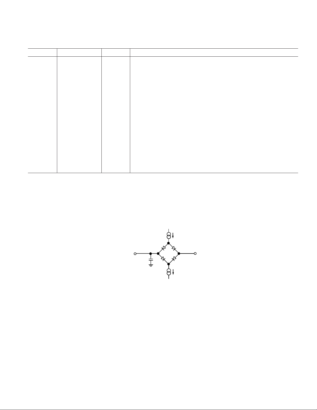
Analog Input
Figure 7 shows an equivalent circuit of the analog input structure of the AD7817 and AD7818. The two diodes D1 and D2
provide ESD protection for the analog inputs. Care must be
taken to ensure that the analog input signal never exceeds the
supply rails by more than 200 mV. This will cause these diodes
to become forward biased and start conducting current into the
IN
substrate. The maximum current these diodes can conduct
without causing irreversible damage to the part is 20 mA. The
capacitor C2 in Figure 7 is typically about 4 pF and can mostly
be attributed to pin capacitance. The resistor R1 is a lumped
component made up of the on resistance of a multiplexer and a
switch. This resistor is typically about 1 kΩ. The capacitor C1 is
the ADC sampling capacitor and has a capacitance of 3 pF.
–11–

AD7816/AD7817/AD7818
V
DD
D1
A
IN
4pF
C2
D2
R1
1k⍀
CONVERT PHASE - SWITCH OPEN
TRACK PHASE - SWITCH CLOSED
C1
3pF
V
BALANCE
Figure 7. Equivalent Analog Input Circuit
DC Acquisition Time
The ADC starts a new acquisition phase at the end of a conversion and ends on the falling edge of the CONVST signal. At the
end of a conversion a settling time is associated with the sampling circuit. This settling time lasts approximately 100 ns. The
analog signal on V
is also being acquired during this settling
IN +
time. Therefore, the minimum acquisition time needed is
approximately 100 ns.
Figure 8 shows the equivalent charging circuit for the sampling
capacitor when the ADC is in its acquisition phase. R2 represents the source impedance of a buffer amplifier or resistive
network, R1 is an internal multiplexer resistance and C1 is the
sampling capacitor.
V
R2
IN
R1
1k⍀
C1
3pF
2.5V
EXTERNAL
REFERENCE
DETECT
BUFFER
1.2V
SW1
REF
IN
1.2V
26k⍀
24k⍀
Figure 9. On-Chip Reference
ADC TRANSFER FUNCTION
The output coding of the AD7816, AD7817, and AD7818 is
straight binary. The designed code transitions occur at successive integer LSB values (i.e., 1 LSB, 2 LSBs, etc.). The LSB
size is = 2.5 V/1024 = 2.44 mV. The ideal transfer characteristic
is shown in Figure 10 below.
111...111
111...110
111...000
011...111
ADC CODE
1LSB=2.5/1024
2.44mV
Figure 8. Equivalent Sampling Circuit
During the acquisition phase the sampling capacitor must be
charged to within a 1/2 LSB of its final value. The time it takes
to charge the sampling capacitor (T
) is given by the
CHARGE
following formula:
T
= 7.6 × (R2 + 1 kΩ) × 3 pF
CHARGE
For small values of source impedance, the settling time associated with the sampling circuit (100 ns) is, in effect, the acquisition time of the ADC. For example, with a source impedance (R2)
of 10 Ω the charge time for the sampling capacitor is approximately 23 ns. The charge time becomes significant for source
impedances of 1 kΩ and greater.
AC Acquisition Time
In ac applications it is recommended to always buffer analog
input signals. The source impedance of the drive circuitry must
be kept as low as possible to minimize the acquisition time of
the ADC. Large values of source impedance will cause the THD
to degrade at high throughput rates.
ON-CHIP REFERENCE
The AD7816, AD7817, and AD7818 have an on-chip 1.2 V
band gap reference that is gained up to give an output of 2.5 V.
The on-chip reference is selected by connecting the REF
IN
pin
to analog ground. This causes SW1 (see Figure 9) to open and
the reference amplifier to power up during a conversion. Therefore, the on-chip reference is not available externally. An external
2.5 V reference can be connected to the REF
pin. This has the
IN
effect of shutting down the on-chip reference circuitry and reduc-
by about 0.25 mA.
ing I
DD
000...010
000...001
000...000
1LSB
0V
ANALOG INPUT
+2.5V•1LSB
Figure 10. ADC Transfer Function
TEMPERATURE MEASUREMENT
The on-chip temperature sensor can be accessed via multiplexer
Channel 0, i.e., by writing 0 0 0 to the channel address register.
The temperature is also the power on default selection. The
transfer characteristic of the temperature sensor is shown in
Figure 11 below. The result of the 10-bit conversion on Channel 0 can be converted to degrees centigrade by using the following equation.
T
= –103°C + (ADC Code/4)
AMB
125°C
TEMPERATURE
–55°C
192Dec 912Dec
ADC CODE
Figure 11. Temperature Sensor Transfer Characteristic
REV. C–12–

AD7816/AD7817/AD7818
TIME – secs
TEMPERATURE – ⴗC
0.50
–0.05
06010 20 30 40 50
0.45
0.30
0.15
0.10
0.05
0.40
0.35
0.25
0.20
0.00
4-LAYER PCB
2-LAYER PCB
TIME – secs
TEMPERATURE – ⴗC
0.25
–0.05
051234
0.15
0.05
0.20
0.10
0.00
4-LAYER PCB
2-LAYER PCB
For example, if the result of a conversion on Channel 0 was
1000000000 (512 Dec), the ambient temperature is equal to
–103°C + (512/4) = +25°C.
Table II below shows some ADC codes for various temperatures.
Table II. Temperature Sensor Output
ADC Code Temperature
00 1100 0000 –55°C
01 0011 1000 –25°C
01 1001 1100 0°C
10 0000 0000 +25°C
10 0111 1000 +55°C
11 1001 0000 +125°C
TEMPERATURE MEASUREMENT ERROR DUE TO REFERENCE ERROR
The AD7816, AD7817, and AD7818 are trimmed using a precision 2.5 V reference to give the transfer function described
previously. To show the effect of the reference tolerance on a
temperature reading, the temperature sensor transfer function
can be rewritten as a function of the reference voltage and the
temperature.
CODE (Dec) = ([113.3285 × K × T]/[q × V
] – 0.6646) × 1024
REF
where:
K = Boltzmann’s Constant, 1.38 × 10
q = Charge on an electron, 1.6 × 10
–23
–19
T =Temperature (K)
So, for example, to calculate the ADC code at 25°C
CODE = ([113.3285
– 0.6646)
×
×
298 × 1.38 × 10
1024
–23
]/[1.6 × 10
–19
× 2.5]
= 511.5 (200 Hex)
As can be seen from the expression, a reference error will produce a gain error. This means that the temperature measurement error due to reference error will be greater at higher
temperatures. For example, with a reference error of –1%, the
measurement error at –55°C would be 2.2 LSBs (0.5°C) and
16 LSBs (4°C) at 125°C.
and temperature sensor (diode) in the package being evaluated.
In Figure 12, the heater (6 mW) is turned off after 30 sec. The
PCB has little influence on the self-heating over the first few
seconds after the heater is turned on. This can be more clearly
seen in Figure 13 where the heater is switched off after 2 seconds. Figure 14 shows the relative effects of self-heating in air,
fluid and in thermal contact with a large heat sink.
These diagrams represent the worst-case effects of self-heating.
The heater delivered 6 mW to the interior of the package in all
cases. This power level is equivalent to the ADC continuously
converting at 100 kSPS. The effects of the self-heating can be
reduced at lower ADC throughput rates by operating on Mode
2 (see Operating Modes section). When operating in this mode,
the on-chip power dissipation reduces dramatically and, as a
consequence, the self-heating effects.
Figure 12. Self-Heating Effect Two-Layer and
Four-Layer PCB
SELF-HEATING CONSIDERATIONS
The AD7817 and AD7818 have an analog-to-digital conversion
function capable of a throughput rate of 100 kSPS. At this
throughput rate the AD7817 and AD7818 will consume between
4 mW and 6.5 mW of power. Because a thermal impedance is
associated with the IC package, the temperature of the die will
rise as a result of this power dissipation. The graphs below show
the self-heating effect in a 16-lead SOIC package. Figures 12
and 13 show the self-heating effect on a two-layer and four-layer
PCB. The plots were generated by assembling a heater (resistor)
REV. C
Figure 13. Self-Heating Effect Two-Layer and
Four-Layer PCB
–13–
AD7816/AD7817/AD7818
0.8
0.7
0.6
0.5
0.4
0.3
0.2
TEMPERATURE – ⴗC
0.1
0.0
–0.01
28
01646 1012
AIR
FLUID
HEAT SINK
14
TIME – secs
Figure 14. Self-Heating Effect in Air, Fluid, and in Thermal
Contact with a Heat Sink
0.25
0.20
0.15
0.10
AIR
FLUID
HEATSINK
OPERATING MODES
The AD7816, AD7817, and AD7818 have two possible modes
of operation depending on the state of the CONVST pulse at
the end of a conversion.
Mode 1
In this mode of operation the CONVST pulse is brought high
before the end of a conversion, i.e., before the BUSY goes low
(see Figure 16). When operating in this mode a new conversion
should not be initiated until 100 ns after the end of a serial read
operation. This quiet time is to allow the track/hold to accurately acquire the input signal after a serial read.
Mode 2
When the AD7816, AD7817, and AD7818 are operated in Mode
2 (see Figure 17), they automatically power down at the end of
a conversion. The CONVST is brought low to initiate a conversion and is left logic low until after the end of the conversion. At
this point, i.e., when BUSY goes low, the devices will powerdown. The devices are powered up again on the rising edge of
the CONVST signal. Superior power performance can be
achieved in this mode of operation by powering up the AD7816,
AD7817, and AD7818 only to carry out a conversion (see Power
vs. Throughput section). In Figure 17 the CS line is applicable
to the AD7817 only.
0.05
TEMPERATURE – ⴗC
0.00
–0.05
0.0 2.00.5 1.5
1.0
TIME – secs
Figure 15. Self-Heating Effect in Air, Fluid, and in Thermal
Contact with a Heat Sink
t
t
2
CONVST
t
3
BUSY
t
17
CS
OTI
RD/ WR
SCLK
1
t
15
t
16
D
IN
D
OUT
DB7 – DB0
DB7(DB9) – DB0
Figure 16. Mode 1 Operation
REV. C–14–

THROUGHPUT – kHz
10
1
0.01
08010
POWER – mW
0.1
20 30 40 50 60 70
CONVST
BUSY
t
POWER-UP
AD7816/AD7817/AD7818
t
1
t
3
CS
OTI
RD/ WR
SCLK
D
IN
D
OUT
DB7 – DB0
Figure 17. Mode 2 Operation
POWER VS. THROUGHPUT
Superior power performance can be achieved by using the Automatic Power-Down (Mode 2) at the end of a conversion (see
Operating Modes section of this data sheet).
CONVST
t
POWER-UP
t
CONVERT
2s 8s
t
15
t
16
DB7(DB9) – DB0
BUSY
t
CYCLE
100s @ 10kSPS
Figure 18. Automatic Power-Down
Figure 18 shows how the Automatic Power-Down is implemented to achieve the optimum power performance from the
AD7816, AD7817, and AD7818. The devices are operated in
Mode 2 and the duration of CONVST pulse is set to be equal to
the power-up time (2 µs). As the throughput rate of the device is
reduced the device remains in its power-down state longer, and
the average power consumption over time drops accordingly.
For example, if the AD7817 is operated in a continuous sampling mode with a throughput rate of 10 kSPS, the power consumption is calculated as follows. The power dissipation during
normal operation is 4.8 mW, VDD = 3 V. If the power up time is
2 µs and the conversion time is 9 µs, the AD7817 can be said to
dissipate 4.8 mW typically for 11 µs (worst case) during each
conversion cycle. If the throughput rate is 10 kSPS, the cycle
time is 100 µs and the power dissipated while powered up dur-
ing each cycle is (11/100) × (4.8 mW) = 528 µW typ. Power
dissipated while powered down during each cycle is (89/100) ×
(3 V × 2 µA) = 5.34 µW typ. Overall power dissipated is 528 µW
+ 5.34 µW = 533 µW.
Figure 19. Power vs. Throughput Rate
AD7817 SERIAL INTERFACE
The serial interface on the AD7817 is a 5-wire interface with
read and write capabilities, with data being read from the output
register via the D
register via the D
line and data being written to the control
OUT
line. The part operates in a slave mode and
IN
requires an externally applied serial clock to the SCLK input to
access data from the data register or write to the control byte.
The RD/WR line is used to determine whether data is being
written to or read from the AD7817. When data is being written
to the AD7817, the RD/WR line is set logic low and when data
is being read from the part the line is set logic high (see Figure
20). The serial interface on the AD7817 is designed to allow the
part to be interfaced to systems that provide a serial clock that is
synchronized to the serial data, such as the 80C51, 87C51,
68HC11, 68HC05, and PIC16Cxx microcontrollers.
REV. C
–15–

AD7816/AD7817/AD7818
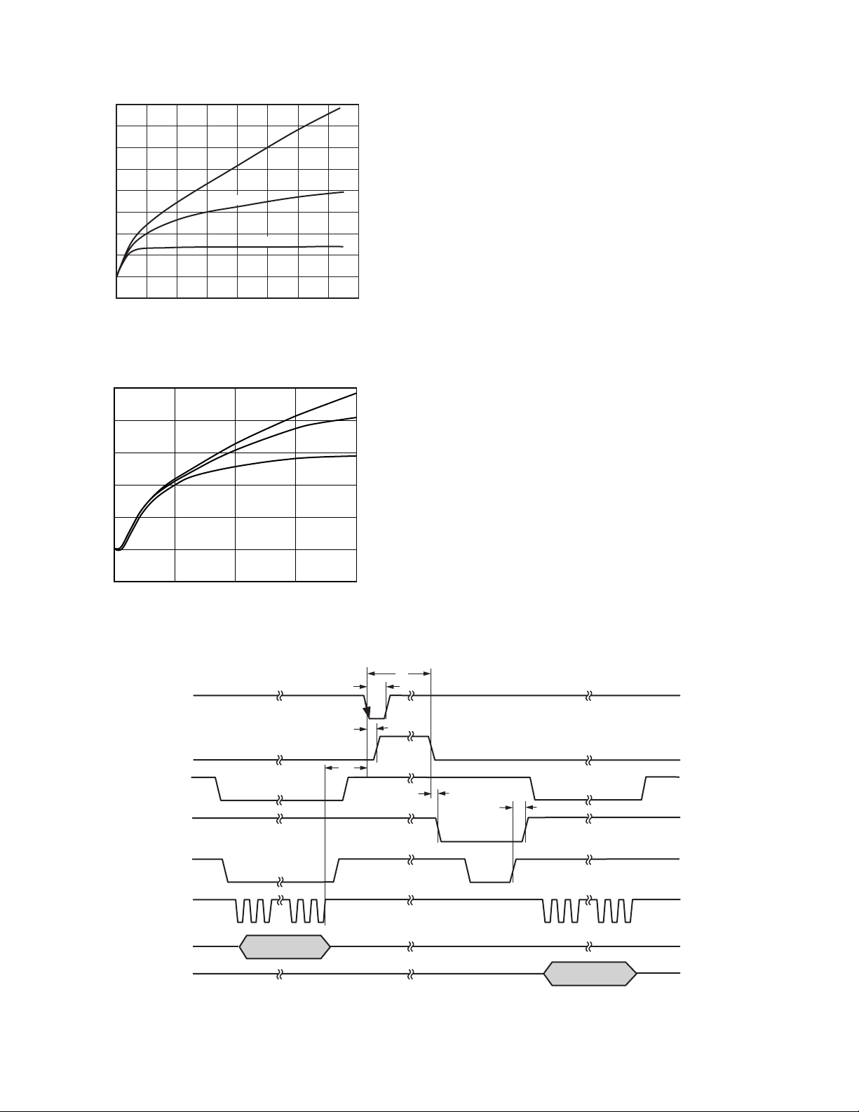
CS
t
4
RD/WR
t
5
SCLK
D
D
OUT
IN
132
t
6
DB7 DB6
t
7
DB5
CONTROL BYTE
t
10
t
8
87
t
9
DB1
DB0
t
11
123
t
12
DB9 DB8 DB7
t
13
Figure 20. AD7817 Serial Interface Timing Diagram
910
DB1
DB0
t
14b
t
14a
Read Operation
Figure 20 shows the timing diagram for a serial read from the
AD7817. CS is brought low to enable the serial interface and RD/
WR is set logic high to indicate that the data transfer is a serial read
from the AD7817. The rising edge of RD/WR clocks out the first
data bit (DB9), subsequent bits are clocked out on the falling edge
of SCLK (except for the first falling SCLK edge) and are valid on
the rising edge. 10 bits of data are transferred during a read operation. However, the user has the choice of clocking only eight bits if
the full 10 bits of the conversion result are not required. The serial
data can be accessed in a number of bytes if 10 bits of data are
being read. However, RD/WR must remain high for the duration of
the data transfer operation. Before starting a new data read operation the RD/WR signal must be brought low and high again. At the
end of the read operation, the D
line enters a high impedance
OUT
state on the rising edge of the CS or the falling edge of RD/WR,
whichever occurs first. The readback process is a destructive
process in that once the data is read back it is erased. A conversion
must be done again; otherwise no data will be read back.
Write Operation
Figure 20 also shows a control byte write operation to the AD7817.
The RD/WR input goes low to indicate to the part that a serial
write is about to occur. The AD7817 control byte is loaded on
the rising edge of the first eight clock cycles of the serial clock
with data on all subsequent clock cycles being ignored. To carry
out a second successive write operation, the RD/WR signal must
be brought high and low again.
Simplifying the Serial Interface
To minimize the number of interconnect lines to the AD7817,
the user can connect the CS line to DGND. This is possible if
the AD7817 is not sharing the serial bus with another device. It
is also possible to tie the D
and D
IN
lines together. This
OUT
arrangement is compatible with the 8051 microcontroller. The
68HC11, 68HC05, and PIC16Cxx can be configured to operate
with a single serial data line. In this way the number of lines
required to operate the serial interface can be reduced to three,
i.e., RD/WR, SCLK, and D
(see Figure 6).
IN/OUT
AD7816 AND AD7818 SERIAL INTERFACE MODE
The serial interface on the AD7816 and AD7818 is a 3-wire
interface with read and write capabilities. Data is read from the
output register and the control byte is written to the AD7816
and AD7818 via the D
line. The part operates in a slave
IN/OUT
mode and requires an externally applied serial clock to the SCLK
input to access data from the data register or write the control
byte. The RD/WR line is used to determine whether data is
being written to or read from the AD7816 and AD7818. When
data is being written to the devices the RD/WR line is set logic
low and when data is being read from the part the line is set
logic high (see Figure 21). The serial interface on the AD7816
and AD7818 are designed to allow the part to be interfaced to
systems that provide a serial clock that is synchronized to the
serial data, such as the 80C51, 87C51, 68HC11, 68HC05, and
PIC16Cxx microcontrollers.
Read Operation
Figure 21 shows the timing diagram for a serial read from the
AD7816 and AD7818. The RD/WR is set logic high to indicate
that the data transfer is a serial read from the devices. When
RD/WR is logic high the D
pin becomes a logic output
IN/OUT
and the first data bit (DB9) appears on the pin. Subsequent bits
are clocked out on the falling edge of SCLK, starting with the
second SCLK falling edge after RD/WR goes high and are valid
on the rising edge of SCLK. Ten bits of data are transferred
during a read operation. However the user has the choice of
clocking only eight bits if the full 10 bits of the conversion result
are not required. The serial data can be accessed in a number of
bytes if 10 bits of data are being read; however, RD/WR must
remain high for the duration of the data transfer operation. To
carry out a successive read operation the RD/WR pin must be
brought logic low and high again. At the end of the read operation, the D
pin becomes a logic input on the falling edge
IN/OUT
of RD/WR.
Write Operation
A control byte write operation to the AD7816 and AD7818 is
also shown in Figure 21. The RD/WR input goes low to indicate
to the part that a serial write is about to occur. The AD7816
and AD7818 control bytes are loaded on the rising edge of the
first eight clock cycles of the serial clock with data on all subsequent clock cycles being ignored. To carry out a successive write
to the AD7816 or AD7818 the RD/WR pin must be brought
logic high and low again.
REV. C–16–

RD/WR
16
9
81
PIN 1
SEATING
PLANE
8ⴗ
0ⴗ
4.50
4.40
4.30
6.40
BSC
5.10
5.00
4.90
0.65
BSC
0.15
0.05
1.20
MAX
0.20
0.09
0.75
0.60
0.45
0.30
0.19
COPLANARITY
0.10
COMPLIANT TO JEDEC STANDARDS MO-153AB
SCLK
DIN/D
OUT
t
5
132
t
6
DB7 DB6
AD7816/AD7817/AD7818
t
8
87
t
t
7
DB5
CONTROL BYTE
9
DB0DB1
Figure 21. AD7816/AD7818 Serial Interface Timing Diagram
OUTLINE DIMENSIONS
t
11
123
t
12
DB9 DB8 DB7
t
13
910
DB0DB1
t
14a
8-Lead Standard Small Outline Package [SOIC]
Narrow Body
(R-8)
Dimensions shown in millimeters and (inches)
5.00 (0.1968)
4.80 (0.1890)
4.00 (0.1574)
3.80 (0.1497)
0.25 (0.0098)
0.10 (0.0040)
COPLANARITY
0.10
CONTROLLING DIMENSIONS ARE IN MILLIMETERS; INCH DIMENSIONS
(IN PARENTHESES) ARE ROUNDED-OFF MILLIMETER EQUIVALENTS FOR
REFERENCE ONLY AND ARE NOT APPROPRIATE FOR USE IN DESIGN
85
1.27 (0.0500)
SEATING
PLANE
COMPLIANT TO JEDEC STANDARDS MS-012AA
BSC
6.20 (0.2440)
5.80 (0.2284)
41
1.75 (0.0688)
1.35 (0.0532)
0.51 (0.0201)
0.31 (0.0122)
0.25 (0.0098)
0.17 (0.0067)
0.50 (0.0196)
0.25 (0.0099)
8ⴗ
0ⴗ
1.27 (0.0500)
0.40 (0.0157)
16-Lead Standard Small Outline Package [SOIC]
Narrow Body
(R-16)
Dimensions shown in millimeters and (inches)
ⴛ 45ⴗ
8-Lead Mini Small Outline Package [MSOP]
(RM-8)
Dimensions shown in millimeters
3.00
BSC
85
3.00
BSC
1
PIN 1
0.65 BSC
0.15
0.00
0.38
0.22
COPLANARITY
0.10
COMPLIANT TO JEDEC STANDARDS MO-187AA
4
SEATING
PLANE
4.90
BSC
1.10 MAX
0.23
0.08
8ⴗ
0ⴗ
0.80
0.60
0.40
16-Lead Thin Shrink Small Outline Package [TSSOP]
(RU-16)
Dimensions shown in millimeters
10.00 (0.3937)
9.80 (0.3858)
4.00 (0.1575)
3.80 (0.1496)
0.25 (0.0098)
0.10 (0.0039)
COPLANARITY
CONTROLLING DIMENSIONS ARE IN MILLIMETERS; INCH DIMENSIONS
(IN PARENTHESES) ARE ROUNDED-OFF MILLIMETER EQUIVALENTS FOR
REFERENCE ONLY AND ARE NOT APPROPRIATE FOR USE IN DESIGN
REV. C
16
1
1.27 (0.0500)
BSC
0.10
COMPLIANT TO JEDEC STANDARDS MS-012AC
1.75 (0.0689)
1.35 (0.0531)
0.51 (0.0201)
0.31 (0.0122)
9
6.20 (0.2441)
5.80 (0.2283)
8
SEATING
PLANE
0.25 (0.0098)
0.17 (0.0067)
0.50 (0.0197)
0.25 (0.0098)
8ⴗ
0ⴗ
1.27 (0.0500)
0.40 (0.0157)
ⴛ 45ⴗ
–17–

AD7816/AD7817/AD7818
Revision History
Location Page
9/04—Data Sheet changed from REV. B to REV. C.
Updated ORDERING GUIDE . . . . . . . . . . . . . . . . . . . . . . . . . . . . . . . . . . . . . . . . . . . . . . . . . . . . . . . . . . . . . . . . . . . . . . . . . . . . . 6
Changes to Operating Modes section . . . . . . . . . . . . . . . . . . . . . . . . . . . . . . . . . . . . . . . . . . . . . . . . . . . . . . . . . . . . . . . . . . . . . . . 13
Changes to Figure 16 . . . . . . . . . . . . . . . . . . . . . . . . . . . . . . . . . . . . . . . . . . . . . . . . . . . . . . . . . . . . . . . . . . . . . . . . . . . . . . . . . . . . 13
Changes to Figure 17 . . . . . . . . . . . . . . . . . . . . . . . . . . . . . . . . . . . . . . . . . . . . . . . . . . . . . . . . . . . . . . . . . . . . . . . . . . . . . . . . . . . . 14
Changes to AD7817 Serial Interface, Read Operation section . . . . . . . . . . . . . . . . . . . . . . . . . . . . . . . . . . . . . . . . . . . . . . . . . . . . . 15
Changes to Figure 20 . . . . . . . . . . . . . . . . . . . . . . . . . . . . . . . . . . . . . . . . . . . . . . . . . . . . . . . . . . . . . . . . . . . . . . . . . . . . . . . . . . . . 15
Changes to Figure 21 . . . . . . . . . . . . . . . . . . . . . . . . . . . . . . . . . . . . . . . . . . . . . . . . . . . . . . . . . . . . . . . . . . . . . . . . . . . . . . . . . . . . 16
REV. C–18–

–19–

C01316–0–9/04(C)
–20–
 Loading...