

REV. B
Information furnished by Analog Devices is believed to be accurate and
reliable. However, no responsibility is assumed by Analog Devices for its
use, nor for any infringements of patents or other rights of third parties
which may result from its use. No license is granted by implication or
otherwise under any patent or patent rights of Analog Devices.
a
AD7814
One Technology Way, P.O. Box 9106, Norwood, MA 02062-9106, U.S.A.
Tel: 781/329-4700 World Wide Web Site: http://www.analog.com
Fax: 781/326-8703 © Analog Devices, Inc., 2000
10-Bit Digital Temperature Sensor
in 6-Lead SOT-23
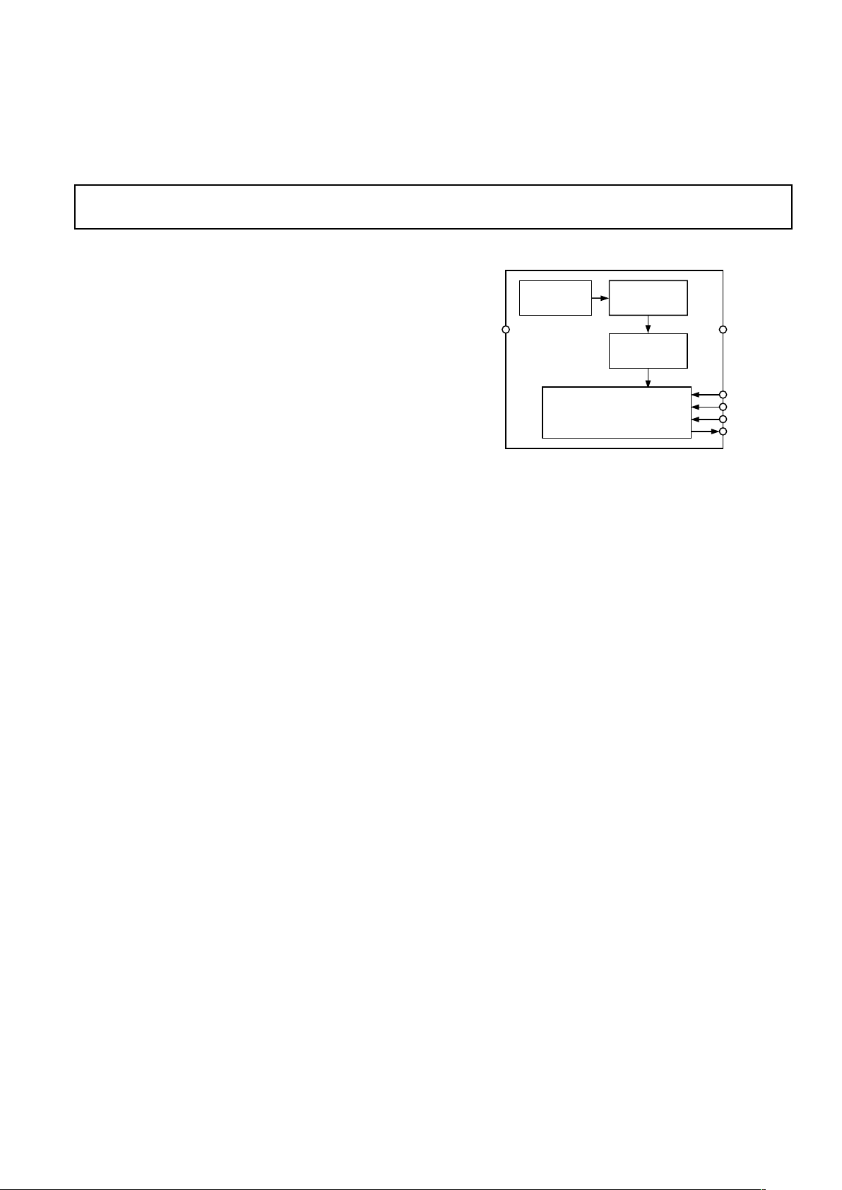
FUNCTIONAL BLOCK DIAGRAM
SERIAL
BUS
INTERFACE
AD7814
V
DD
CS
SCLK
DIN
DOUT
GND
TEMPERATURE
VALUE
REGISTER
10-BIT
ANALOG/DIGITAL
CONVERTER
BANDGAP
TEMPERATURE
SENSOR
FEATURES
10-Bit Temperature-to-Digital Converter
–55ⴗC to +125ⴗC Operating Temperature Range
ⴞ2ⴗC Accuracy
SPI- and DSP-Compatible Serial Interface
Shutdown Mode
Space-Saving SOT-23 Package
APPLICATIONS
Hard Disk Drives
Personal Computers
Electronic Test Equipment
Office Equipment
Domestic Appliances
Process Control
GENERAL DESCRIPTION
The AD7814 is a complete temperature monitoring system in
an SOT-23 package or 8-lead µSOIC package. It contains a
bandgap temperature sensor and 10-bit ADC to monitor and
digitize the temperature reading to a resolution of +0.25°C.
The AD7814 has a flexible serial interface that allows easy interfacing to most microcontrollers. The interface is compatible
with SPI™, QSPI and MICROWIRE™ protocol and is also
compatible with DSPs. The part features a standby mode that is
controlled via the serial interface.
The AD7814’s wide supply voltage range, low supply current
and SPI-compatible interface, make it ideal for a variety of applications, including personal computers, office equipment, and
domestic appliances.
SPI is a trademark of Motorola, Inc.
MICROWIRE is a trademark of National Semiconductor, Inc.
PRODUCT HIGHLIGHTS
1. The AD7814 has an on-chip temperature sensor that allows
an accurate measurement of the ambient temperature. The
measurable temperature range is –55°C to +125°C, with a
± 2°C temperature accuracy.
2. Supply voltage of +2.7 V to +5.5 V.
3. Space-saving 6-lead SOT-23 package and 8-lead µSOIC
package.
4. 10-bit temperature reading to +0.25°C resolution.
5. The AD7814 features a standby mode that reduces the
current consumption to 1 µA.

REV. B
–2–
AD7814–SPECIFICATIONS
1, 2
Parameter Min Typ Max Units Test Conditions/Comments
TEMPERATURE SENSOR AND ADC
Accuracy ± 2.0 °CT
A
= 0°C to +85°C. VDD = +3 V to +5.5 V
3
± 2.5 °CT
A
= –40°C to 0°C. VDD = +3 V to +5.5 V
3
± 2.0 ± 3.5 °CT
A
= –55°C to +125°C. VDD = +3 V to +5.5 V
Resolution 10 Bits
Update Rate, t
R
400 µs
Temperature Conversion Time 25 µs
SUPPLIES
Supply Voltage 2.7 5.5 V For Specified Performance
Supply Current
Normal Mode 250 400 µA
Shutdown Mode 1 3 µA
Power Dissipation 80 µWV
DD
= +3 V. Using Normal Mode
Power Dissipation V
DD
= +3 V. Using Shutdown Mode
1 sps 3 µW
10 sps 3.3 µW
100 sps 6 µW
DIGITAL INPUT
Input High Voltage, V
IH
2.4 V
Input Low Voltage, V
IL
0.8 V
Input Current, I
IN
± 1 µAV
IN
= 0 V to V
DD
Input Capacitance, C
IN
10 pF All Digital Inputs
DIGITAL OUTPUT
Output High Voltage, V
OH
VDD – 0.3 V I
SOURCE
= I
SINK
= 200 µA
Output Low Voltage, V
OL
0.4 V IOL = 200 µA
Output Capacitance, C
OUT
50 pF
NOTES
1
All specifications apply for –55°C to +125°C unless otherwise stated.
2
Guaranteed by design and characterization, not production tested.
3
For VDD = +2.7 V to +3 V and TA = –40°C to +85°C, the typical temperature error is ±2°C.
Specifications subject to change without notice.
TIMING CHARACTERISTICS
1, 2, 3
Parameter Limit Units Comments
t
1
0 ns min CS to SCLK Setup Time
t
2
50 ns min SCLK High Pulsewidth
t
3
50 ns min SCLK Low Pulsewidth
t
4
4
35 ns max Data Access Time After SCLK Falling Edge
t
5
20 ns min Data Setup Time Prior to SCLK Rising Edge
t
6
0 ns min Data Hold Time After SCLK Rising Edge
t
7
0 ns min CS to SCLK Hold Time
t
8
4
40 ns max CS to DOUT High Impedance
NOTES
1
Guaranteed by design and characterization, not production tested.
2
All input signals are specified with tr = tf = 5 ns (10% to 90% of VDD) and timed from a voltage level of 1.6 V.
3
See Figure 2.
4
Measured with the load circuit of Figure 1.
(TA = T
MIN
to T
MAX
, VDD = +2.7 V to +5.5 V, unless otherwise noted)
(TA = T
MIN
to T
MAX
, VDD = +2.7 V to +5.5 V, unless otherwise noted)

REV. B
AD7814
–3–
ORDERING GUIDE
Temperature Temperature Package Branding Package
Model Range Error* Description Information Option
AD7814ART –55°C to +125°C ± 2°C 6-Lead SOT-23 CAA RT-6
AD7814ARM –55°C to +125°C ± 2°C 8-Lead µSOIC CAA RM-8
*Temperature error is over 0°C to +85°C temperature range.
ABSOLUTE MAXIMUM RATINGS*
VDD to GND . . . . . . . . . . . . . . . . . . . . . . . . . . –0.3 V to +7 V
Digital Input Voltage to GND . . . . . . . –0.3 V to V
DD
+ 0.3 V
Digital Output Voltage to GND . . . . . –0.3 V to V
DD
+ 0.3 V
Operating Temperature Range . . . . . . . . . . –55°C to +125°C
Storage Temperature Range . . . . . . . . . . . . –65°C to +150°C
Junction Temperature . . . . . . . . . . . . . . . . . . . . . . . . +150°C
SOT-23, Power Dissipation . . . . . . . . . . . . . . . . . . . . 450 mW
θ
JA
Thermal Impedance . . . . . . . . . . . . . . . . . . . . 240°C/W
Lead Temperature, Soldering
Vapor Phase (60 sec) . . . . . . . . . . . . . . . . . . . . . +215°C
Infrared (15 sec) . . . . . . . . . . . . . . . . . . . . . . . . . +220°C
µSOIC Package, Power Dissipation . . . . . . . . . . . . . . 450 mW
θ
JA
Thermal Impedance . . . . . . . . . . . . . . . . . . . . 206°C/W
Lead Temperature, Soldering
Vapor Phase (60 sec) . . . . . . . . . . . . . . . . . . . . . +215°C
Infrared (15 sec) . . . . . . . . . . . . . . . . . . . . . . . . . +220°C
*Stresses above those listed under Absolute Maximum Ratings may cause perma-
nent damage to the device. This is a stress rating only; functional operation of the
device at these or any other conditions above those indicated in the operational
section of this specification is not implied. Exposure to absolute maximum rating
conditions for extended periods may affect device reliability.
CAUTION
ESD (electrostatic discharge) sensitive device. Electrostatic charges as high as 4000 V readily
accumulate on the human body and test equipment and can discharge without detection.
Although the AD7814 features proprietary ESD protection circuitry, permanent damage may
occur on devices subjected to high energy electrostatic discharges. Therefore, proper ESD
precautions are recommended to avoid performance degradation or loss of functionality.
WARNING!
ESD SENSITIVE DEVICE
+1.6V
I
OL
200A
200A
I
OH
TO
OUTPUT
PIN
C
L
50pF
Figure 1. Load Circuit for Data Access Time and Bus
Relinquish Time
 Loading...