

2.7 V to 5.5 V, 400 kSPS
a
FEATURES
8-/10-Bit ADC with 2.3 s Conversion Time
On-Chip Track and Hold
Operating Supply Range: 2.7 V to 5.5 V
Specifications at 2.7 V– 3.6 V and 5 V 10%
8-Bit Parallel Interface
8-Bit + 2-Bit Read
Power Performance
Normal Operation
10.5 mW, V
Automatic Power-Down
34.6 W @ 1 kSPS, V
Analog Input Range: 0 V to V
Reference Input Range: 1.2 V to V
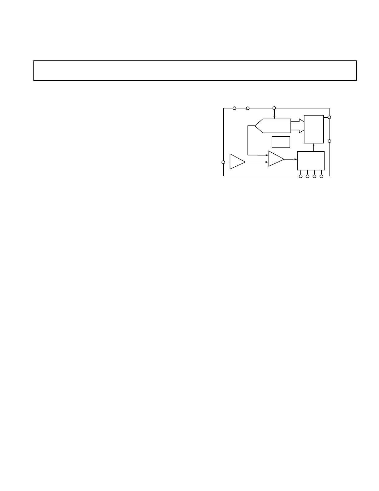
GENERAL DESCRIPTION
The AD7813 is a high-speed, microprocessor-compatible,
8-/10-bit analog-to-digital converter with a maximum throughput of 400 kSPS. The converter operates off a single 2.7 V to
5.5 V supply and contains a 2.3 µs successive approximation
A/D converter, track/hold circuitry, on-chip clock oscillator and
8-bit wide parallel interface. The parallel interface is designed to
allow easy interfacing to microprocessors and DSPs. The 10-bit
conversion result is read by carrying out two 8-bit read operations. The first read operation accesses the 8 MSBs of the ADC
conversion result and the second read accesses the 2 LSBs.
Using only address decoding logic the AD7813 is easily mapped
into the microprocessor address space.
When used in its power-down mode, the AD7813 automatically
powers down at the end of a conversion and powers up at the
start of a new conversion. This feature significantly reduces the
power consumption of the part at lower throughput rates. The
AD7813 can also operate in a high speed mode where the part is
not powered down between conversions. In this mode of operation the part is capable of providing 400 kSPS throughput.
The part is available in a small, 16-lead, 0.3" wide, plastic dualin-line package (DIP), in a 16-lead, 0.15" wide, narrow body
small outline IC (SOIC) and in a 16-lead thin shrink small
outline package (TSSOP).
= 3 V
DD
= 3 V
DD
REF
DD
8-/10-Bit Sampling ADC
AD7813
FUNCTIONAL BLOCK DIAGRAM
V
AGND
DD
AD7813
V
T/H
IN
PRODUCT HIGHLIGHTS
1. Low Power, Single Supply Operation
The AD7813 operates from a single 2.7 V to 5.5 V supply
and typically consumes only 10.5 mW of power. The power
dissipation can be significantly reduced at lower throughput rates by using the automatic power-down mode.
2. Automatic Power-Down
The automatic power-down mode, whereby the AD7813
goes into power-down mode at the end of a conversion and
powers up before the next conversion, means the AD7813
is ideal for battery powered applications; e.g., 34.6 µW
@ 1 kSPS. (See Power vs. Throughput Rate section.)
3. Parallel Interface
An easy to use 8-bit-wide parallel interface allows interfacing
to most popular microprocessors and DSPs with minimal
external circuitry.
4. Dynamic Specifications for DSP Users
In addition to the traditional ADC specifications, the AD7813
is specified for ac parameters, including signal-to-noise ratio
and distortion.
V
REF
CHARGE
REDISTRIBUTION
DAC
CLOCK
OSC
COMP
BUSY
THREE-
STATE
DRIVERS
CONTROL
LOGIC
CS RD
DB7
DB0
CONVST
REV. C
Information furnished by Analog Devices is believed to be accurate and
reliable. However, no responsibility is assumed by Analog Devices for its
use, nor for any infringements of patents or other rights of third parties
which may result from its use. No license is granted by implication or
otherwise under any patent or patent rights of Analog Devices.
One Technology Way, P.O. Box 9106, Norwood, MA 02062-9106, U.S.A.
Tel: 781/329-4700 World Wide Web Site: http://www.analog.com
Fax: 781/326-8703 © Analog Devices, Inc., 2000

AD7813–SPECIFICATIONS
(GND = 0 V, V
1
+105C unless otherwise noted.)
= VDD = 3 V 10% to 5 V 10%. All specifications –40C to
REF
Parameter Y Version Unit Test Conditions/Comments
DYNAMIC PERFORMANCE f
Signal to (Noise + Distortion) Ratio
Total Harmonic Distortion (THD)
Peak Harmonic or Spurious Noise
Intermodulation Distortion
2
1
1
1
58 dB min
–66 dB max
–66 dB max
= 30 kHz, f
IN
fa = 29.1 kHz, fb = 29.8 kHz
2nd Order Terms –67 dB typ
3rd Order Terms –67 dB typ
DC ACCURACY
Resolution 10 Bits
Minimum Resolution for Which
No Missing Codes Are Guaranteed 10 Bits
Relative Accuracy
Differential Nonlinearity (DNL)
Gain Error
Offset Error
1
1
1
1
± 1 LSB max
± 1 LSB max
± 2 LSB max
± 2.0 LSB max
ANALOG INPUT
Input Voltage Range 0 V min
V
Input Leakage Current
Input Capacitance
REFERENCE INPUTS
V
Input Voltage Range 1.2 V min
REF
2
2
2
REF
± 1 µA max
20 pF max
V
DD
V max
V max
Input Leakage Current ± 3 µA max
Input Capacitance 15 pF max
LOGIC INPUTS
V
Input High Voltage 2.0 V min
INH,
V
Input Low Voltage 0.4 V max (0.8 V max, VDD = 5 V)
INL,
Input Current, I
Input Capacitance, C
2
IN
IN
± 1 µA max Typically 10 nA, VIN = 0 V to V
8 pF max
LOGIC OUTPUTS
Output High Voltage, V
Output Low Voltage, V
OL
OH
2.4 V min I
0.4 V max I
SOURCE
= 200 µA
SINK
= 200 µA
High Impedance Leakage Current ± 1 µA max
High Impedance Capacitance 15 pF max
SAMPLE
= 350 kHz
DD
CONVERSION RATE
Conversion Time 2.3 µs max
Track/Hold Acquisition Time
1
100 ns max
POWER SUPPLY
V
DD
I
DD
2.7–5.5 Volts For Specified Performance
Normal Operation 3.5 mA max
Power-Down 1 µA max V
Power Dissipation
Normal Operation 17.5 mW max V
Power-Down 5 µW max
Auto Power-Down V
1 kSPS Throughput 34.6 µW max
10 kSPS Throughput 346.5 µW max
100 kSPS Throughput 3.46 mW max
NOTES
1
See Terminology section.
2
Sample tested during initial release and after any redesign or process change that may affect this parameter.
Specifications subject to change without notice.
–2–
Digital Inputs = 0 V or V
= 5 V
DD
= 5 V
DD
= 3 V
DD
DD
REV. C
1, 2
WARNING!
ESD SENSITIVE DEVICE
TIMING CHARACTERISTICS
(–40C to +105C, unless otherwise noted)
Parameter VDD = 3 V 10% VDD = 5 V 10% Unit Conditions/Comments
AD7813
t
POWER-UP
t
1
t
2
t
3
t
4
t
5
3
t
6
3, 4
t
7
1.5 1.5 µs (max) Power-Up Time of AD7813 after Rising Edge of CONVST.
2.3 2.3 µs (max) Conversion Time.
20 20 ns (min) CONVST Pulsewidth.
30 30 ns (max) CONVST Falling Edge to BUSY Rising Edge Delay.
0 0 ns (min) CS to RD Setup Time.
0 0 ns (min) CS Hold Time after RD High.
10 10 ns (max) Data Access Time after RD Low.
10 10 ns (max) Bus Relinquish Time after RD High.
5 5 ns (min)
t
8
3
t
9
NOTES
1
Sample tested to ensure compliance.
2
See Figures 12, 13 and 14.
3
These numbers are measured with the load circuit of Figure 1. They are defined as the time required for the o/p to cross 0.8 V or 2.4 V for VDD = 5 V ± 10% and
0.4 V or 2 V for VDD = 3 V ± 10%.
4
Derived from the measured time taken by the data outputs to change 0.5 V when loaded with the circuit of Figure 1. The measured number is then extrapolated back
to remove the effects of charging or discharging the 50 pF capacitor. This means that the time, t
of the part and as such is independent of external bus loading capacitances.
10 10 ns (min) Minimum Time Between MSB and LSB Reads.
50 50 ns (min) Rising Edge of CS or RD to Falling Edge of CONVST Delay.
, quoted in the Timing Characteristics is the true bus relinquish time
7
ABSOLUTE MAXIMUM RATINGS*
VDD to DGND . . . . . . . . . . . . . . . . . . . . . . . . . –0.3 V to +7 V
200AI
OL
Digital Input Voltage to DGND
(CONVST, RD, CS) . . . . . . . . . . . . . . –0.3 V, V
Digital Output Voltage to DGND
(BUSY, DB0–DB7) . . . . . . . . . . . . . . . –0.3 V, V
to AGND . . . . . . . . . . . . . . . . . . . –0.3 V, V
REF
IN
Analog Input . . . . . . . . . . . . . . . . . . . . . . –0.3 V, V
+ 0.3 V
DD
+ 0.3 V
DD
+ 0.3 V
DD
+ 0.3 V
DD
OUTPUT
PIN
TO
50pF
C
L
200A
I
OH
1.6V
Storage Temperature Range . . . . . . . . . . . . –65°C to +150°C
Junction Temperature . . . . . . . . . . . . . . . . . . . . . . . . . . 150°C
Plastic DIP Package, Power Dissipation . . . . . . . . . . 450 mW
Thermal Impedance . . . . . . . . . . . . . . . . . . . . 105°C/W
θ
JA
Figure 1. Load Circuit for Digital Output Timing
Specifications
Lead Temperature, (Soldering 10 sec) . . . . . . . . . . . . 260°C
SOIC Package, Power Dissipation . . . . . . . . . . . . . . . 450 mW
Thermal Impedance . . . . . . . . . . . . . . . . . . . . . 75°C/W
θ
JA
Lead Temperature, Soldering
Vapor Phase (60 sec) . . . . . . . . . . . . . . . . . . . . . . . 215°C
Infrared (15 sec) . . . . . . . . . . . . . . . . . . . . . . . . . . 220°C
SSOP Package, Power Dissipation . . . . . . . . . . . . . . . 450 mW
Thermal Impedance . . . . . . . . . . . . . . . . . . . . 115°C/W
θ
JA
Lead Temperature, Soldering
Vapor Phase (60 sec) . . . . . . . . . . . . . . . . . . . . . . . 215°C
Model Error Description Option
AD7813YN ± 1 LSB Plastic DIP N-16
AD7813YR ±1 LSB Small Outline IC R-16A
AD7813YRU ± 1 LSB Thin Shrink Small Outline RU-16
ORDERING GUIDE
Linearity Package Package
(TSSOP)
Infrared (15 sec) . . . . . . . . . . . . . . . . . . . . . . . . . . 220°C
*Stresses above those listed under Absolute Maximum Ratings may cause perma-
nent damage to the device. This is a stress rating only; functional operation of the
device at these or any other conditions above those listed in the operational sections
of this specification is not implied. Exposure to absolute maximum rating conditions for extended periods may affect device reliability.
CAUTION
ESD (electrostatic discharge) sensitive device. Electrostatic charges as high as 4000 V readily
accumulate on the human body and test equipment and can discharge without detection. Although
the AD7813 features proprietary ESD protection circuitry, permanent damage may occur on
devices subjected to high-energy electrostatic discharges. Therefore, proper ESD precautions are
recommended to avoid performance degradation or loss of functionality.
REV. C
–3–
AD7813
Pin
No. Mnemonic Description
PIN FUNCTION DESCRIPTIONS
1V
2V
REF
IN
Reference Input, 1.2 V to VDD.
Analog Input, 0 V to V
REF
.
3 GND Analog and Digital Ground.
4 CONVST Convert Start. A low-to-high transition on this pin initiates a 1.5 µs pulse on an internally generated
CONVST signal. A high-to-low transition on this line initiates the conversion process if the internal
CONVST signal is low. Depending on the signal on this pin at the end of a conversion, the AD7813
automatically powers down.
5 CS Chip Select. This is a logic input. CS is used in conjunction with RD to enable outputs.
6 RD Read Pin. This is a logic input. When CS is low and RD goes low, the DB7–DB0 leave their high
impedance state and data is driven onto the data bus.
7 BUSY ADC Busy Signal. This is a logic output. This signal goes logic high during the conversion process.
8–15 DB0–DB7 Data Bit 0 to 7. These outputs are three-state TTL-compatible.
16 V
DD
Positive power supply voltage, 2.7 V to 5.5 V.
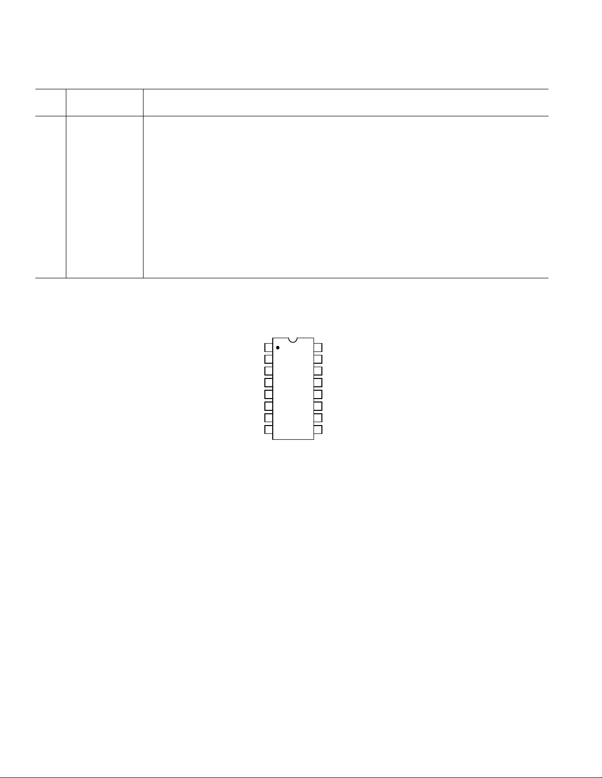
PIN CONFIGURATION
DIP/SOIC
V
REF
V
GND
CONVST
CS
RD
BUSY
DB0
1
2
IN
3
4
5
6
7
8
AD7813
TOP VIEW
(Not to Scale)
V
16
DD
DB7
15
DB6
14
DB5
13
DB4
12
DB3
11
DB2
10
DB1
9
–4–
REV. C

AD7813
TERMINOLOGY
Signal to (Noise + Distortion) Ratio
This is the measured ratio of signal to (noise + distortion) at the
output of the A/D converter. The signal is the rms amplitude of
the fundamental. Noise is the rms sum of all nonfundamental
signals up to half the sampling frequency (f
/2), excluding dc.
S
The ratio is dependent upon the number of quantization levels
in the digitization process; the more levels, the smaller the quantization noise. The theoretical signal to (noise + distortion) ratio
for an ideal N-bit converter with a sine wave input is given by:
Signal to (Noise + Distortion) = (6.02N + 1.76) dB
Thus for an 10-bit converter, this is 62 dB.
Total Harmonic Distortion
Total harmonic distortion (THD) is the ratio of the rms sum of
harmonics to the fundamental. For the AD7813 it is defined as:
2
2
2
2
2
+ V
5
6
THD (dB ) = 20 log
V
+ V
+ V
2
3
+ V
4
V
1
where V1 is the rms amplitude of the fundamental and V2, V3,
V
, V5 and V6 are the rms amplitudes of the second through the
4
sixth harmonics.
Peak Harmonic or Spurious Noise
Peak harmonic or spurious noise is defined as the ratio of the
rms value of the next largest component in the ADC output
spectrum (up to f
/2 and excluding dc) to the rms value of the
S
fundamental. Normally, the value of this specification is determined by the largest harmonic in the spectrum, but for parts
where the harmonics are buried in the noise floor, it will be a
noise peak.
Intermodulation Distortion
With inputs consisting of sine waves at two frequencies, fa and
fb, any active device with nonlinearities will create distortion
products at sum and difference frequencies of mfa ± nfb where
m, n = 0, 1, 2, 3, etc. Intermodulation terms are those for which
neither m nor n are equal to zero. For example, the second
order terms include (fa + fb) and (fa – fb), while the third order
terms include (2fa + fb), (2fa – fb), (fa + 2fb) and (fa – 2fb).
The AD7813 is tested using the CCIF standard, where two
input frequencies near the top end of the input bandwidth are
used. In this case, the second and third order terms are of different significance. The second order terms are usually distanced
in frequency from the original sine waves, while the third order
terms are usually at a frequency close to the input frequencies.
As a result, the second and third order terms are specified separately. The calculation of the intermodulation distortion is as
per the THD specification where it is the ratio of the rms sum
of the individual distortion products to the rms amplitude of the
fundamental expressed in dBs.
Relative Accuracy
Relative accuracy or endpoint nonlinearity is the maximum
deviation from a straight line passing through the endpoints of
the ADC transfer function.
Differential Nonlinearity
This is the difference between the measured and the ideal
1 LSB change between any two adjacent codes in the ADC.
Offset Error
This is the deviation of the first code transition (0000 . . . 000)
to (0000 . . . 001) from the ideal, i.e., AGND + 1 LSB.
Offset Error Match
This is the difference in Offset Error between any two channels.
Gain Error
This is the deviation of the last code transition (1111 . . . 110)
to (1111 . . . 111) from the ideal, i.e., VREF – 1 LSB, after the
offset error has been adjusted out.
Gain Error Match
This is the difference in Gain Error between any two channels.
Track/Hold Acquisition Time
Track/hold acquisition time is the time required for the output
of the track/hold amplifier to reach its final value, within
± 1/2 LSB, after the end of conversion (the point at which the
track/hold returns to track mode). It also applies to situations
where a change in the selected input channel takes place or
where there is a step input change on the input voltage applied
to the selected V
input of the AD7813. It means that the user
IN
must wait for the duration of the track/hold acquisition time
after the end of conversion, or after a step input change to V
,
IN
before starting another conversion, to ensure that the part
operates to specification.
REV. C
–5–

AD7813
V
IN
R1
125
R2
C1
3.5pF
CIRCUIT DESCRIPTION
Converter Operation
The AD7813 is a successive approximation analog-to-digital
converter based around a charge redistribution DAC. The ADC
can convert analog input signals in the range 0 V to V
DD
. Figures 2 and 3 below show simplified schematics of the ADC.
Figure 2 shows the ADC during its acquisition phase. SW2 is
closed and SW1 is in Position A, the comparator is held in a
balanced condition and the sampling capacitor acquires the
signal on V
V
IN
AGND
.
IN+
CHARGE
REDISTRIBUTION
SAMPLING
CAPACITOR
A
+
SW1
B
ACQUISITION
PHASE
V
/3
DD
SW2
COMPARATOR
DAC
CONTROL
LOGIC
CLOCK
OSC
Figure 2. ADC Track Phase
When the ADC starts a conversion (see Figure 3), SW2 will
open and SW1 will move to Position B, causing the comparator
to become unbalanced. The Control Logic and the Charge
Redistribution DAC are used to add and subtract fixed amounts
of charge from the sampling capacitor so as to bring the comparator back into a balanced condition. When the comparator is
rebalanced the conversion is complete. The Control Logic generates the ADC output code. Figure 7 shows the ADC transfer
function.
CHARGE
REDISTRIBUTION
DAC
CONTROL
LOGIC
CLOCK
OSC
V
IN
AGND
SAMPLING
CAPACITOR
A
+
SW1
B
CONVERSION
PHASE
V
/3
DD
SW2
COMPARATOR
Figure 3. ADC Conversion Phase
TYPICAL CONNECTION DIAGRAM
Figure 4 shows a typical connection diagram for the AD7813. The
parallel interface is implemented using an 8-bit data bus, the
falling edge of CONVST brings the BUSY signal high, and at
the end of conversion the falling edge of BUSY is used to initiate an Interrupt Service Routine (ISR) on a microprocessor—
see Parallel Interface section for more details. V
to a well decoupled V
0 V to V
. When VDD is first connected the AD7813 powers
DD
pin to provide an analog input range of
DD
is connected
REF
up in a low current mode, i.e., power-down. A rising edge on an
internal CONVST input will cause the part to power up—see
Power-Up Times. If power consumption is of concern, the
automatic power-down at the end of a conversion should be
used to improve power performance. See Power vs. Throughput
Rate section of the data sheet.
SUPPLY
2.7V TO 5.5V
0V TO V
REF
INPUT
0.1F10F
BUSY
RD
CS
PARALLEL
INTERFACE
C/
P
VDDV
AD7813
V
IN
GND
REF
DB0-DB7
CONVST
Figure 4. Typical Connection Diagram
Analog Input
Figure 5 shows an equivalent circuit of the analog input structure of the AD7813. The two diodes, D1 and D2, provide ESD
protection for the analog inputs. Care must be taken to ensure
that the analog input signal never exceeds the supply rails by
more than 200 mV. This will cause these diodes to become
forward biased and start conducting current into the substrate.
The maximum current these diodes can conduct without causing irreversible damage to the part is 20 mA. The capacitor C2,
in Figure 5, is typically about 4 pF and can be primarily attributed to pin capacitance. The resistor R1 is a lumped component
made up of the on resistance of a multiplexer and a switch. This
resistor is typically about 125 Ω. The capacitor C1 is the ADC
sampling capacitor and has a capacitance of 3.5 pF.
V
DD
D1
V
IN
4pF
C2
CONVERT PHASE – SWITCH OPEN
D2
TRACK PHASE – SWITCH CLOSED
R1
125
C1
3.5pF
/3
V
DD
Figure 5. Equivalent Analog Input Circuit
DC Acquisition Time
The ADC starts a new acquisition phase at the end of a conversion and ends on the falling edge of the CONVST signal. At the
end of a conversion there is a settling time associated with the
sampling circuit. This settling time lasts approximately 100 ns.
The analog signal on V
is also being acquired during this settling
IN
time; therefore, the minimum acquisition time needed is
approximately 100 ns.
Figure 6 shows the equivalent charging circuit for the sampling
capacitor when the ADC is in its acquisition phase. R2 represents the source impedance of a buffer amplifier or resistive
network, R1 is an internal multiplexer resistance and C1 is the
sampling capacitor.
Figure 6. Equivalent Sampling Circuit
–6–
REV. C

AD7813
During the acquisition phase the sampling capacitor must be
charged to within a 1/2 LSB of its final value. The time it takes
to charge the sampling capacitor (T
) is given by the
CHARGE
following formula:
T
= 7.6 × (R2 + 125 Ω) × 3.5 pF
CHARGE
For small values of source impedance, the settling time associated with the sampling circuit (100 ns) is, in effect, the acquisition time of the ADC. For example, with a source impedance
(R2) of 10 Ω the charge time for the sampling capacitor is
approximately 4 ns. The charge time becomes significant for
source impedances of 2 kΩ and greater.
AC Acquisition Time
In ac applications it is recommended to always buffer analog
input signals. The source impedance of the drive circuitry must
be kept as low as possible to minimize the acquisition time of
the ADC. Large values of source impedance will cause the
THD to degrade at high throughput rates.
ADC TRANSFER FUNCTION
The output coding of the AD7813 is straight binary. The
designed code transitions occur at successive integer LSB values
(i.e., 1 LSB, 2 LSBs, etc.). The LSB size is = V
/1024. The
REF
ideal transfer characteristic for the AD7813 is shown in Figure 7.
111...111
111...110
111...000
011...111
ADC CODE
000...010
000...001
000...000
1LSB = V
1LSB
0V
ANALOG INPUT
/1024
REF
+V
–1LSB
REF
Figure 7. Transfer Characteristic
POWER-UP TIMES
The AD7813 has a 1.5 µs power-up time. When VDD is first
connected, the AD7813 is in a low current mode of operation.
In order to carry out a conversion the AD7813 must first be
powered up. The ADC is powered up by a rising edge on an
internally generated CONVST signal, which occurs as a result
of a rising edge on the external CONVST pin. The rising edge
of the external CONVST signal initiates a 1.5 µs pulse on the
internal CONVST signal. This pulse is present to ensure the
part has enough time to power up before a conversion is initiated, as a conversion is initiated on the falling edge of gated
CONVST. See Timing and Control section. Care must be taken
to ensure that the CONVST pin of the AD7813 is logic low
when V
is first applied.
DD
When operating in Mode 2, the ADC is powered down at the
end of each conversion and powered up again before the next
conversion is initiated. (See Figure 8.)
MODE 1
V
DD
EXT CONVST
t
POWER-UP
1.5s
INT CONVST
MODE 2
V
DD
EXT CONVST
INT CONVST
t
POWER-UP
1.5s
t
POWER-UP
1.5s
Figure 8. Power-Up Times
POWER VS. THROUGHPUT RATE
By operating the AD7813 in Mode 2, the average power consumption of the AD7813 decreases at lower throughput rates.
Figure 9 shows how the Automatic Power-Down is implemented
using the external CONVST signal to achieve the optimum
power performance for the AD7813. The AD7813 is operated
in Mode 2, and the duration of the external CONVST pulse is
set to be equal to or less than the power-up time of the device.
As the throughput rate is reduced, the device remains in its powerdown state longer and the average power consumption over time
drops accordingly.
EXT CONVST
t
POWER-UP
t
1.5s
INT CONVST
CONVERT
2.3s
100s @ 10kSPS
POWER-DOWN
t
CYCLE
Figure 9. Automatic Power-Down
For example, if the AD7813 is operated in a continuous sampling mode, with a throughput rate of 10 kSPS, the power consumption is calculated as follows. The power dissipation during
normal operation is 10.5 mW, V
= 3 V. If the power-up time
DD
is 1.5 µs and the conversion time is 2.3 µs, the AD7813 can then
be said to dissipate 10.5 mW for 3.8 µs (worst-case) during each
conversion cycle. If the throughput rate is 10 kSPS, the cycle
time is 100 µs and the average power dissipated during each
cycle is (3.8/100) × (10.5 mW) = 400 µW.
REV. C
–7–

AD7813
Typical Performance Characteristics
10
1
POWER – mW
0.1
0.01
0505 1015202530354045
Figure 10. Power vs. Throughput
0
–10
–20
–30
–40
–50
dBs
–60
–70
–80
–90
–100
0 17417 35 52 70 87 105 122 140 157
TIMING AND CONTROL
The AD7813 has only one input for timing and control, i.e.,
the CONVST (convert start signal). The rising edge of this
CONVST signal initiates a 1.5 µs pulse on an internally gener-
ated CONVST signal. This pulse is present to ensure the part
has enough time to power up before a conversion is initiated. If
the external CONVST signal is low, the falling edge of the
internal CONVST signal will cause the sampling circuit to go
into hold mode and initiate a conversion. If, however, the external CONVST signal is high when the internal CONVST goes
low, it is upon the falling edge of the external CONVST signal
that the sampling circuitry will go into hold mode and initiate a
conversion. The use of the internally generated 1.5 µs pulse,
as previously described, can be likened to the configuration
shown in Figure 12. The application of a CONVST signal at
the CONVST pin triggers the generation of a 1.5 µs pulse. Both
the external CONVST and this internal CONVST are input to
an OR gate. The resulting signal has the duration of the longer
of the two input signals. Once a conversion has been initiated
the BUSY signal goes high to indicate a conversion is in progress.
THROUGHPUT – kSPS
AD7813
2048 POINT FFT
SAMPLING 357.142kHz
30.168kHz
f
IN
FREQUENCY – kHz
Figure 11. SNR
At the end of conversion the sampling circuit goes back into its
tracking mode again. The end of conversion is indicated by the
BUSY signal going low. This signal may be used to initiate an
ISR on a microprocessor. At this point the conversion result is
latched into the output register where it may be read. The AD7813
has an 8-bit wide parallel interface. The 10-bit conversion result
is accessed by performing two successive read operations. The
first 8-bit read accesses the 8 MSBs of the conversion result and
the second read accesses the 2 LSBs, as illustrated in Figure 13,
where one performance of the two successive reads is highlighted
after the falling edge of BUSY. The state of the external CONVST
signal at the end of conversion also establishes the mode of operation of the AD7813.
Mode 1 Operation (High Speed Sampling)
If the external CONVST is logic high when BUSY goes low, the
part is said to be in Mode 1 operation. While operating in Mode
1, the AD7813 will not power down between conversions. The
AD7813 should be operated in Mode 1 for high speed sampling
applications, i.e., throughputs greater than 100 kSPS. Figure 13
shows the timing for Mode 1 operation. From this diagram one
can see that a minimum delay of the sum of the conversion time
and read time must be left between two successive falling edges
of the external CONVST. This is to ensure that a conversion is
not initiated during a read.
Mode 2 Operation (Automatic Power-Down)
At slower throughput rates the AD7813 may be powered down
between conversions to give a superior power performance.
This is Mode 2 Operation and it is achieved by bringing the
CONVST signal logic low before the falling edge of BUSY.
Figure 14, overleaf, shows the timing for Mode 2 Operation.
The falling edge of the external CONVST signal may occur
before or after the falling edge of the internal CONVST signal,
but it is the later occurring falling edge of both that controls
when the first conversion will take place. If the falling edge
of the external CONVST occurs after that of the internal
CONVST, it means that the moment of the first conversion is
controlled exactly, regardless of any jitter associated with the
internal CONVST signal. The parallel interface is still fully
operational while the AD7813 is powered down. The AD7813
is powered up again on the rising edge of the CONVST signal.
The gated CONVST pulse will now remain high long enough
for the AD7813 to fully power up, which takes about 1.5 µs. This
is ensured by the internal CONVST signal, which will remain high
for 1.5 µs.
CONVST
(PIN 4)
1.5s
EXT
GATED
INT
Figure 12.
–8–
REV. C

EXT CONVST
INT CONVST
BUSY
CS/RD
t
POWER-UP
AD7813
t
t
2
t
3
1
DB7–DB0
Figure 13. Mode 1 Operation
EXT CONVST
t
INT CONVST
BUSY
CS/RD
DB7–DB0
POWER-UP
t
3
t
1
Figure 14. Mode 2 Operation
PARALLEL INTERFACE
The parallel interface of the AD7813 is eight bits wide. The
output data buffers are activated when both CS and RD are
logic low. At this point the contents of the data register are
placed on the 8-bit data bus. Figure 15 shows the timing diagram for the parallel port. As previously explained, two successive read operations must take place in order to access the 10-bit
conversion result. The first read places the 8 MSBs on the data
bus and the second read places the 2 LSBs on the data bus. The
2 LSBs appear on DB7 and DB6, with DB5–DB0 set to logic zero.
8 MSBs
8 MSBs
2 LSBs
Further read operations will access the 8 MSBs and 2 LSBs of
the 10-bit ADC conversion result again. The parallel interface
of the AD7813 is reset when BUSY goes logic high. This feature
allows the AD7813 to be used as an 8-bit converter if the user
only wishes to access the 8 MSBs of the conversion. Care must
be taken to ensure that a read operation does not occur while
BUSY is high. Data read from the AD7813 while BUSY is high
will be invalid. For optimum performance the read operation
should end at least 100 ns (t
) prior to the falling edge of the
10
next CONVST.
REV. C
CONVST
BUSY
CS
RD
DB7–DB0
t
t
3
2
t
1
t
4
t
6
8 MSBs 2 MSBs
t
8
t
5
t
7
t
9
Figure 15. Parallel Port Timing
–9–

AD7813
MICROPROCESSOR INTERFACING
The parallel port on the AD7813 allows the device to be interfaced to a range of many different microcontrollers. This section
explains how to interface the AD7813 with some of the more
common microcontroller parallel interface protocols.
AD7813 to 8051
Figure 16 shows a parallel interface between the AD7813 and
the 8051 microcontroller. The BUSY signal on the AD7813 provides an interrupt request to the 8051 when a conversion begins.
Port 0 of the 8051 may serve as an input or output port, or as in
this case when used together, may be used as a bidirectional
low-order address and data bus. The address latch enable output of the 8051 is used to latch the low byte of the address during accesses to the device, while the high-order address byte is
supplied from Port 2. Port 2 latches remain stable when the
AD7813 is addressed, as they do not have to be turned around
(set to 1) for data input as is the case for Port 0.
8051*
DB0–DB7
PSP0–PSP7
PIC16C6x/7x*
CS
RD
INT
*
ADDITIONAL PINS OMITTED FOR CLARITY
DB0–DB7
AD7813
CS
RD
BUSY
*
Figure 17. Interfacing to the PIC16C6x/7x
AD7813 to ADSP-21xx
Figure 18 shows a parallel interface between the AD7813 and
the ADSP-21xx series of DSPs. As before, the BUSY signal on
the AD7813 provides an interrupt request to the DSP when a
conversion begins.
AD0–AD7
ALE
A8–A15
RD
INT
*
ADDITIONAL PINS OMITTED FOR CLARITY
LATCH
DECODER
CS
RD
BUSY
AD7813
*
Figure 16. Interfacing to the 8051
AD7813 to PIC16C6x/7x
Figure 17 shows a parallel interface between the AD7813 and the
PIC16C64/65/74. The BUSY signal on the AD7813 provides
an interrupt request to the microcontroller when a conversion
begins. Of the PIC16C6x/7x range of microcontrollers only the
PIC16C64/65/74 can provide the option of a parallel slave port.
Port D of the microcontroller will operate as an 8-bit wide
parallel slave port when control bit PSPMODE in the TRISE
register is set. Setting PSPMODE enables the port pin RE0
to be the RD output and RE2 to be the CS output. For this
functionality, the corresponding data direction bits of the
TRISE register must be configured as outputs (reset to 0).
See PIC16/17 Microcontroller User Manual.
D7–D0
A13–A0
ADSP-21xx*
DMS
RD
IRQ
*
ADDITIONAL PINS OMITTED FOR CLARITY
ADDRESS
EN
DECODE
LOGIC
Figure 18. Interfacing to the ADSP-21xx
DB0–DB7
AD7813
CS
RD
BUSY
*
–10–
REV. C

0.210 (5.33)
MAX
0.160 (4.06)
0.115 (2.93)
0.1574 (4.00)
0.1497 (3.80)
OUTLINE DIMENSIONS
Dimensions shown in inches and (mm).
16-Lead Plastic DIP
(N-16)
0.840 (21.33)
0.745 (18.93)
16
18
PIN 1
0.022 (0.558)
0.014 (0.356)
0.100
(2.54)
BSC
9
0.280 (7.11)
0.240 (6.10)
0.060 (1.52)
0.015 (0.38)
0.070 (1.77)
0.045 (1.15)
SEATING
PLANE
16-Lead Small Outline Package
(R-16A)
0.3937 (10.00)
0.3859 (9.80)
16 9
0.2550 (6.20)
81
0.2284 (5.80)
0.130
(3.30)
MIN
0.325 (8.25)
0.300 (7.62)
0.015 (0.381)
0.008 (0.204)
AD7813
0.195 (4.95)
0.115 (2.93)
C01005–0–10/00 (rev. C)
0.0098 (0.25)
0.0040 (0.10)
SEATING
PLANE
PIN 1
0.0500
(1.27)
BSC
0.0688 (1.75)
0.0532 (1.35)
0.0192 (0.49)
0.0138 (0.35)
0.0099 (0.25)
0.0075 (0.19)
0.0196 (0.50)
0.0099 (0.25)
8°
0°
0.0500 (1.27)
0.0160 (0.41)
16-Lead Thin Shrink Small Outline Package
(RU-16)
0.201 (5.10)
0.193 (4.90)
0.177 (4.50)
0.006 (0.15)
0.002 (0.05)
SEATING
PLANE
16
0.169 (4.30)
1
PIN 1
0.0256
(0.65)
BSC
0.0118 (0.30)
0.0075 (0.19)
9
8
0.256 (6.50)
0.246 (6.25)
0.0433
(1.10)
MAX
0.0079 (0.20)
0.0035 (0.090)
8°
0°
0.028 (0.70)
0.020 (0.50)
x 45°
PRINTED IN U.S.A.
REV. C
–11–
 Loading...