Analog Devices AD7813 Datasheet

+2.7 V to +5.5 V, 400 kSPS
a
FEATURES
8-/10-Bit ADC with 2.3 s Conversion Time
On-Chip Track and Hold
Operating Supply Range: +2.7 V to +5.5 V
Specifications at 2.7 V–3.6 V and 5 V 10%
8-Bit Parallel Interface
8-Bit + 2-Bit Read
Power Performance
Normal Operation
10.5 mW, V
Automatic Power-Down
34.6 W @ 1 kSPS, V
Analog Input Range: 0 V to V
Reference Input Range: 1.2 V to V
GENERAL DESCRIPTION
The AD7813 is a high-speed, microprocessor-compatible,
8-/10-bit analog-to-digital converter with a maximum throughput of 400 kSPS. The converter operates off a single +2.7 V to
+5.5 V supply and contains a 2.3 µs successive approximation
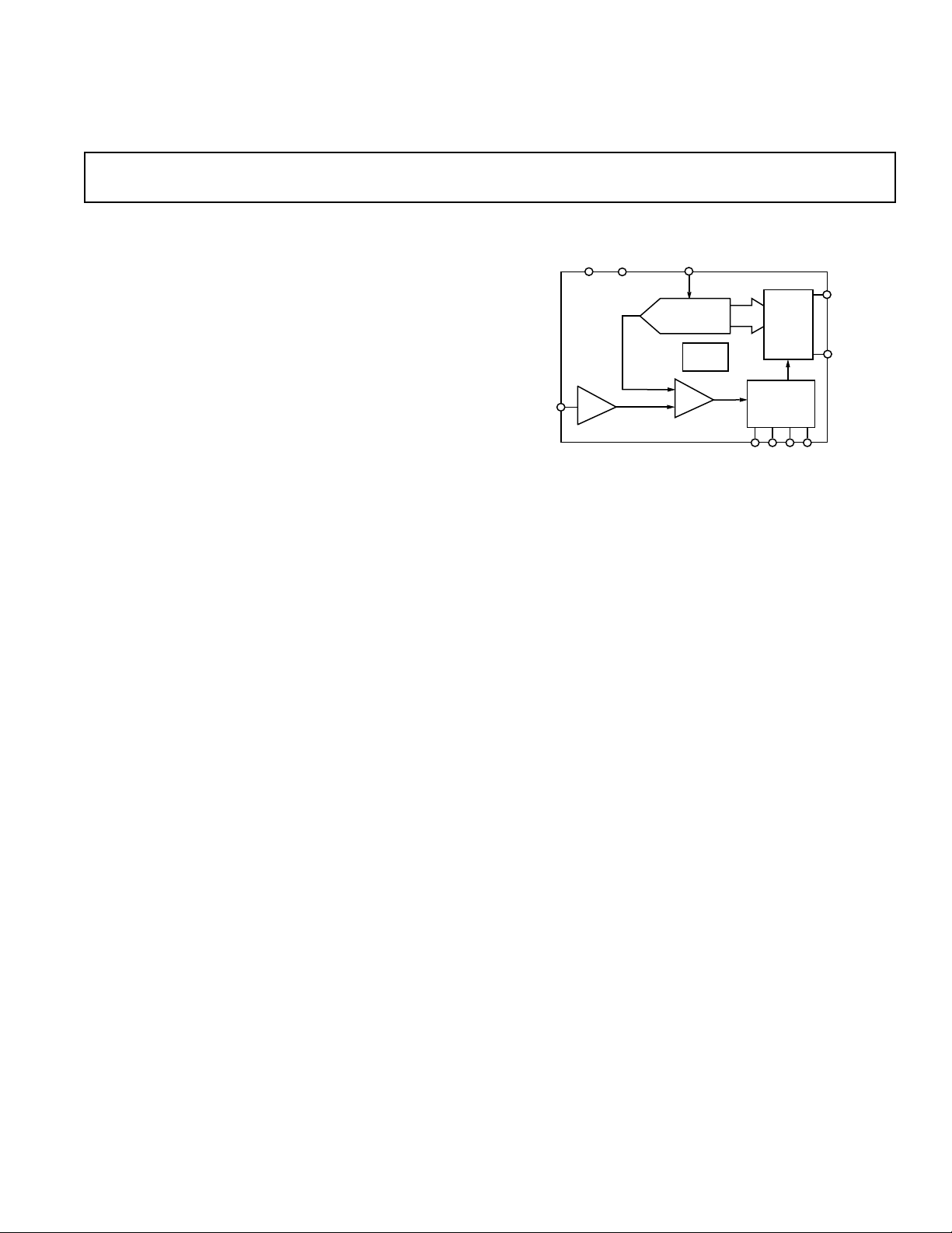
A/D converter, track/hold circuitry, on-chip clock oscillator and
8-bit wide parallel interface. The parallel interface is designed to
allow easy interfacing to microprocessors and DSPs. The 10-bit
conversion result is read by carrying out two 8-bit read operations. The first read operation accesses the 8 MSBs of the ADC
conversion result and the second read accesses the 2 LSBs.
Using only address decoding logic the AD7813 is easily mapped
into the microprocessor address space.
When used in its power-down mode, the AD7813 automatically
powers down at the end of a conversion and powers up at the
start of a new conversion. This feature significantly reduces the
power consumption of the part at lower throughput rates. The
AD7813 can also operate in a high speed mode where the part is
not powered down between conversions. In this mode of operation the part is capable of providing 400 kSPS throughput.
The part is available in a small, 16-lead, 0.3" wide, plastic dualin-line package (DIP), in a 16-lead, 0.15" wide, narrow body
small outline IC (SOIC) and in a 16-lead thin shrink small
outline package (TSSOP).
= 3 V
DD
DD
= 3 V
REF
DD
8-/10-Bit Sampling ADC
AD7813
FUNCTIONAL BLOCK DIAGRAM
V
AGND
DD
AD7813
V
T/H
IN
PRODUCT HIGHLIGHTS
1. Low Power, Single Supply Operation
The AD7813 operates from a single +2.7 V to +5.5 V supply and typically consumes only 10.5 mW of power. The
power dissipation can be significantly reduced at lower
throughput rates by using the automatic power-down mode.
2. Automatic Power-Down
The automatic power-down mode, whereby the AD7813
goes into power-down mode at the end of a conversion and
powers up before the next conversion, means the AD7813
is ideal for battery powered applications; e.g., 34.6 µW
@ 1 kSPS. (See Power vs. Throughput Rate section.)
3. Parallel Interface
An easy to use 8-bit-wide parallel interface allows interfacing
to most popular microprocessors and DSPs with minimal
external circuitry.
4. Dynamic Specifications for DSP Users
In addition to the traditional ADC specifications, the AD7813
is specified for ac parameters, including signal-to-noise ratio
and distortion.
V
REF
CHARGE
REDISTRIBUTION
DAC
CLOCK
OSC
COMP
BUSY
THREE-
STATE
DRIVERS
CONTROL
LOGIC
CS RD
DB7
DB0
CONVST
REV. B
Information furnished by Analog Devices is believed to be accurate and
reliable. However, no responsibility is assumed by Analog Devices for its
use, nor for any infringements of patents or other rights of third parties
which may result from its use. No license is granted by implication or
otherwise under any patent or patent rights of Analog Devices.
One Technology Way, P.O. Box 9106, Norwood, MA 02062-9106, U.S.A.
Tel: 781/329-4700 World Wide Web Site: http://www.analog.com
Fax: 781/326-8703 © Analog Devices, Inc., 2000

AD7813–SPECIFICATIONS
(GND = 0 V, V
1
+105C unless otherwise noted.)
= +VDD = 3 V 10% to 5 V 10%. All specifications –40C to
REF
Parameter Y Version Un it Test Conditions/Comments
DYNAMIC PERFORMANCE f
Signal to (Noise + Distortion) Ratio
Total Harmonic Distortion (THD)
Peak Harmonic or Spurious Noise
Intermodulation Distortion
2
1
1
1
58 dB min
–66 dB max
–66 dB max
= 30 kHz, f
IN
fa = 29.1 kHz, fb = 29.8 kHz
2nd Order Terms –67 dB typ
3rd Order Terms –67 dB typ
DC ACCURACY
Resolution 10 Bits
Minimum Resolution for Which
No Missing Codes Are Guaranteed 10 Bits
Relative Accuracy
Differential Nonlinearity (DNL)
Gain Error
Offset Error
1
1
1
1
± 1 LSB max
± 1 LSB max
± 2 LSB max
± 2.0 LSB max
ANALOG INPUT
Input Voltage Range 0 V min
V
Input Leakage Current
Input Capacitance
REFERENCE INPUTS
V
Input Voltage Range 1.2 V min
REF
2
2
2
REF
± 1 µA max
20 pF max
V
DD
V max
V max
Input Leakage Current ± 3 µA max
Input Capacitance 15 pF max
LOGIC INPUTS
V
Input High Voltage 2.0 V min
INH,
V
Input Low Voltage 0.4 V max (0.8 V max, VDD = 5 V)
INL,
Input Current, I
Input Capacitance, C
2
IN
IN
± 1 µA max Typically 10 nA, VIN = 0 V to V
8 pF max
LOGIC OUTPUTS
Output High Voltage, V
Output Low Voltage, V
OL
OH
2.4 V min I
0.4 V max I
SOURCE
= 200 µA
SINK
= 200 µA
High Impedance Leakage Current ± 1 µA max
High Impedance Capacitance 15 pF max
SAMPLE
= 350 kHz
DD
CONVERSION RATE
Conversion Time 2.3 µs max
Track/Hold Acquisition Time
1
100 ns max
POWER SUPPLY
V
DD
I
DD
2.7–5.5 Volts For Specified Performance
Normal Operation 3.5 mA max
Power-Down 1 µA max V
Power Dissipation
Normal Operation 17.5 mW max V
Power-Down 5 µW max
Auto Power-Down V
1 kSPS Throughput 34.6 µW max
10 kSPS Throughput 346.5 µW max
100 kSPS Throughput 3.46 mW max
NOTES
1
See Terminology section.
2
Sample tested during initial release and after any redesign or process change that may affect this parameter.
Specifications subject to change without notice.
–2–
Digital Inputs = 0 V or V
= 5 V
DD
= 5 V
DD
= 3 V
DD
DD
REV. B

1, 2
TIMING CHARACTERISTICS
(–40C to +105C, unless otherwise noted)
Parameter VDD = 3 V 10% VDD = 5 V 10% Unit Conditions/Comments
AD7813
t
POWER-UP
t
1
t
2
t
3
t
4
t
5
3
t
6
3, 4
t
7
11 µs (max) Power-Up Time of AD7813 after Rising Edge of CONVST.
2.3 2.3 µs (max) Conversion Time.
20 20 ns (min) CONVST Pulsewidth.
30 30 ns (max) CONVST Falling Edge to BUSY Rising Edge Delay.
0 0 ns (min) CS to RD Setup Time.
0 0 ns (min) CS Hold Time after RD High.
10 10 ns (max) Data Access Time after RD Low.
10 10 ns (max) Bus Relinquish Time after RD High.
5 5 ns (min)
t
8
3
t
9
NOTES
1
Sample tested to ensure compliance.
2
See Figures 12, 13 and 14.
3
These numbers are measured with the load circuit of Figure 1. They are defined as the time required for the o/p to cross 0.8 V or 2.4 V for VDD = 5 V ± 10% and
0.4 V or 2 V for VDD = 3 V ± 10%.
4
Derived from the measured time taken by the data outputs to change 0.5 V when loaded with the circuit of Figure 1. The measured number is then extrapolated back
to remove the effects of charging or discharging the 50 pF capacitor. This means that the time, t
of the part and as such is independent of external bus loading capacitances.
10 10 ns (min) Minimum Time Between MSB and LSB Reads.
50 50 ns (min) Rising Edge of CS or RD to Falling Edge of CONVST Delay.
, quoted in the Timing Characteristics is the true bus relinquish time
7
ABSOLUTE MAXIMUM RATINGS*
VDD to DGND . . . . . . . . . . . . . . . . . . . . . . . . . –0.3 V to +7 V
200AI
OL
Digital Input Voltage to DGND
(CONVST, RD, CS) . . . . . . . . . . . . . . –0.3 V, V
Digital Output Voltage to DGND
(BUSY, DB0–DB7) . . . . . . . . . . . . . . . –0.3 V, V
to AGND . . . . . . . . . . . . . . . . . . . –0.3 V, V
REF
IN
Analog Input . . . . . . . . . . . . . . . . . . . . . . –0.3 V, V
+ 0.3 V
DD
+ 0.3 V
DD
+ 0.3 V
DD
+ 0.3 V
DD
TO
OUTPUT
PIN
50pF
C
L
200A
I
OH
+1.6V
Storage Temperature Range . . . . . . . . . . . . –65°C to +150°C
Junction Temperature . . . . . . . . . . . . . . . . . . . . . . . . .+150°C
Plastic DIP Package, Power Dissipation . . . . . . . . . . 450 mW
Thermal Impedance . . . . . . . . . . . . . . . . . . . +105°C/W
θ
JA
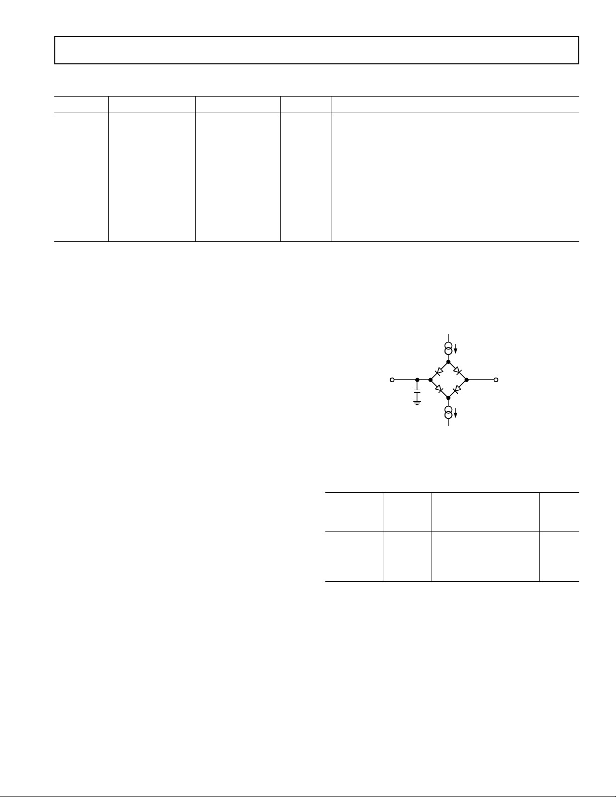
Figure 1. Load Circuit for Digital Output Timing
Specifications
Lead Temperature, (Soldering 10 sec) . . . . . . . . . . .+260°C
SOIC Package, Power Dissipation . . . . . . . . . . . . . . . 450 mW
Thermal Impedance . . . . . . . . . . . . . . . . . . . . . 75°C/W
θ
JA
Lead Temperature, Soldering
Vapor Phase (60 sec) . . . . . . . . . . . . . . . . . . . . . .+215°C
Infrared (15 sec) . . . . . . . . . . . . . . . . . . . . . . . . .+220°C
SSOP Package, Power Dissipation . . . . . . . . . . . . . . . 450 mW
Thermal Impedance . . . . . . . . . . . . . . . . . . . . 115°C/W
θ
JA
Lead Temperature, Soldering
Vapor Phase (60 sec) . . . . . . . . . . . . . . . . . . . . . .+215°C
Infrared (15 sec) . . . . . . . . . . . . . . . . . . . . . . . . .+220°C
Model (LSB) Description Option
AD7813YN ± 1 LSB Plastic DIP N-16
AD7813YR ±1 LSB Small Outline IC R-16A
AD7813YRU ± 1 LSB Thin Shrink Small Outline RU-16
ORDERING GUIDE
Linearity
Error Package Package
(TSSOP)
ESD . . . . . . . . . . . . . . . . . . . . . . . . . . . . . . . . . . . . . . . . ≥4 kV
*Stresses above those listed under Absolute Maximum Ratings may cause perma-
nent damage to the device. This is a stress rating only; functional operation of the
device at these or any other conditions above those listed in the operational sections
of this specification is not implied. Exposure to absolute maximum rating conditions for extended periods may affect device reliability.
REV. B
–3–

AD7813
Pin
No. Mnemonic Description
PIN FUNCTION DESCRIPTIONS
1V
2V
REF
IN
Reference Input, 1.2 V to VDD.
Analog Input, 0 V to V
REF
.
3 GND Analog and Digital Ground.
4 CONVST Convert Start. A low-to-high transition on this pin initiates a 1 µs pulse on an internally generated
CONVST signal. A high-to-low transition on this line initiates the conversion process if the internal
CONVST signal is low. Depending on the signal on this pin at the end of a conversion, the AD7813
automatically powers down.
5 CS Chip Select. This is a logic input. CS is used in conjunction with RD to enable outputs.
6 RD Read Pin. This is a logic input. When CS is low and RD goes low, the DB7–DB0 leave their high
impedance state and data is driven onto the data bus.
7 BUSY ADC Busy Signal. This is a logic output. This signal goes logic high during the conversion process.
8–15 DB0–DB7 Data Bit 0 to 7. These outputs are three-state TTL-compatible.
16 V
DD
Positive power supply voltage, +2.7 V to +5.5 V.
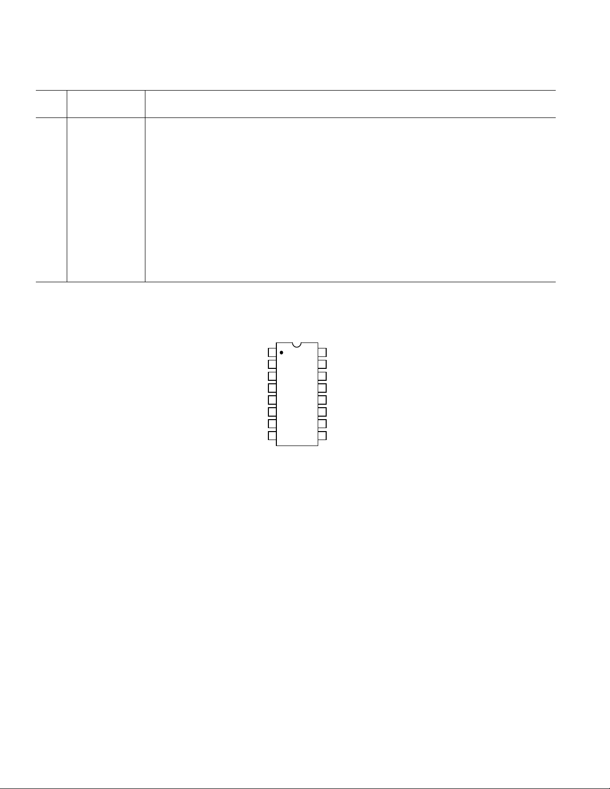
PIN CONFIGURATION
DIP/SOIC
V
REF
V
GND
CONVST
CS
RD
BUSY
DB0
1
2
IN
3
4
5
6
7
8
AD7813
TOP VIEW
(Not to Scale)
V
16
DD
DB7
15
DB6
14
DB5
13
DB4
12
DB3
11
DB2
10
DB1
9
–4–
REV. B
 Loading...