

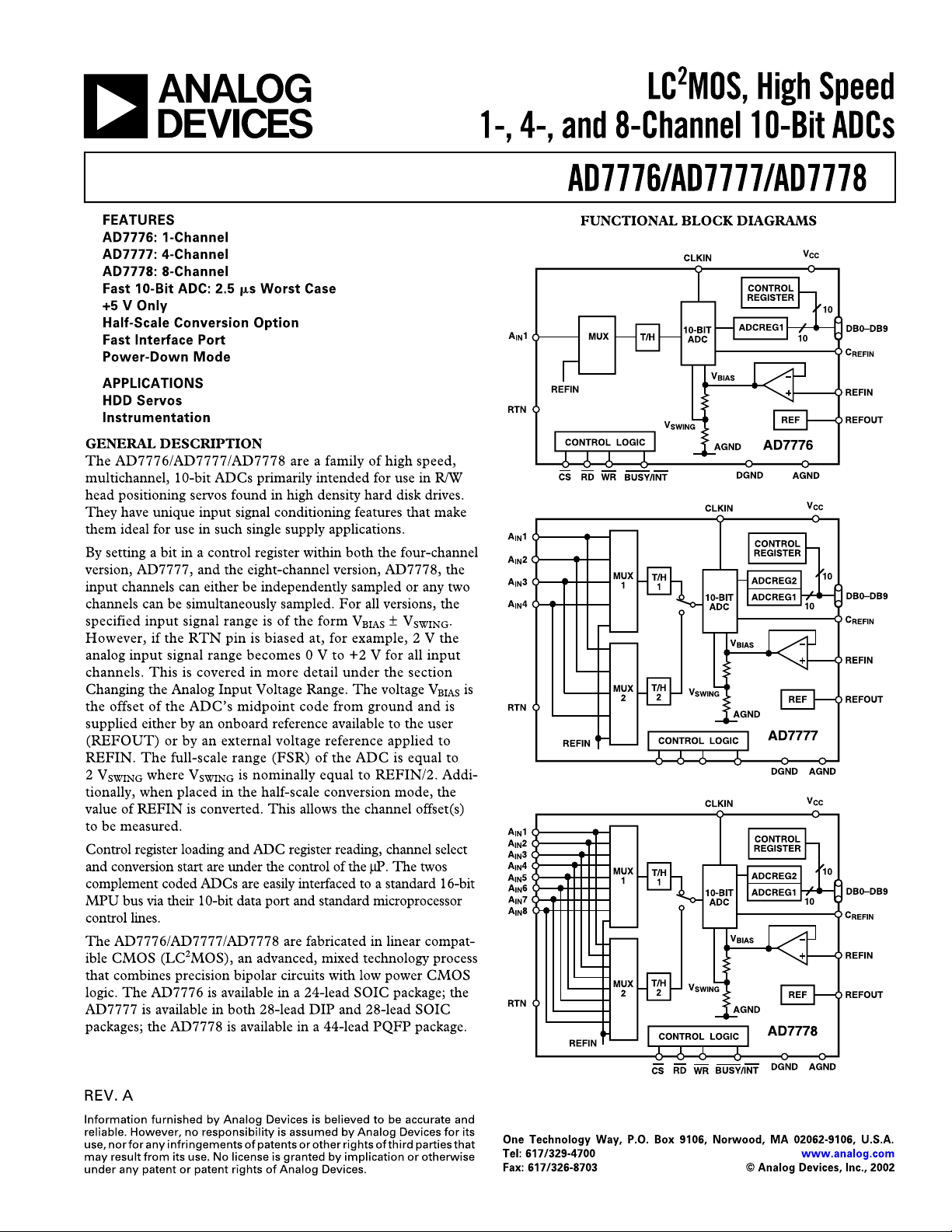

AD7776/AD7777/AD7778–SPECIFICATIONS
CLKIN = 8 MHz; RTN = O V; C
Parameter A Versions
= 10 nF; all specifications T
REFIN
to T
MIN
1
Units Conditions/Comments
unless otherwise noted.)
MAX
(VCC = +5 V ⴞ 5%; AGND = DGND = O V;
DC ACCURACY
Resolution
2
10 Bits
Relative Accuracy ± 1 LSB max See Terminology
Differential Nonlinearity ± 1 LSB max No Missing Codes; See Terminology
Bias Offset Error ± 12 LSB max See Terminology
Bias Offset Error Match 10 LSB max Between Channels, AD7777/AD7778 Only; See Terminology
Plus or Minus Full-Scale Error ± 12 LSB max See Terminology
Plus or Minus Full-Scale Error Match 10 LSB max Between Channels, AD7777/AD7778 Only; See Terminology
ANALOG INPUTS
Input Voltage Range
All Inputs V
BIAS
± V
SWING
Input Current +200 µA max VIN = V
V min/V max
BIAS
± V
; Any Channel
SWING
REFERENCE INPUT
REFIN 1.9/2.1 V min/V max For Specified Performance
REFIN Input Current +200 µA max
REFERENCE OUTPUT
REFOUT 1.9/2.1 V min/V max Nominal REFOUT = 2.0 V
DC Output Impedance 5 Ω typ
Reference Load Change ± 2 mV max For Reference Load Current Change of 0 to ± 500 µA
± 5 mV max For Reference Load Current Change of 0 to ± 1 mA
Short Circuit Current
3
20 mA max See Terminology
Reference Load Should Not Change During Conversion
LOGIC OUTPUTS
DB0–DB9, BUSY/INT
, Output Low Voltage 0.4 V max I
V
OL
, Output High Voltage 4.0 V min I
V
OH
Floating State Leakage Current ± 10 µA max
Floating State Capacitance
3
10 pF max
= 1.6 mA
SINK
SOURCE
= 200 µA
ADC Output Coding Twos Complement
LOGIC INPUTS
DB0–DB9, CS, WR, RD, CLKIN
Input Low Voltage, V
Input High Voltage, V
Input Leakage Current 10 µA max
Input Capacitance
INL
INH
3
0.8 V max
2.4 V min
10 pF max
CONVERSION TIMING
Acquisition Time 4.5 t
Single Conversion 14 t
Double Conversion 28 t
t
CLKIN
High 50 ns min Minimum High Time for CLKIN
t
CLKIN
t
Low 40 ns min Minimum Low Time for CLKIN
CLKIN
CLKIN
5.5 t
+ 70 ns max
CLKIN
CLKIN
CLKIN
125/500 ns min/ns max Period of Input Clock CLKIN
ns min See Terminology
ns max
ns max
POWER REQUIREMENTS
Range 4.75/5.25 V min/V max For Specified Performance
V
CC
, Normal Mode 15 mA max CS = RD = +5 V, CR8 = 0
I
CC
, Power-Down Mode 1.5 mA max CR8 = 1. All Linear Circuitry OFF
I
CC
Power-Up Time to Operational
Specifications 500 µs max From Power-Down Mode
DYNAMIC PERFORMANCE See Terminology
Signal to Noise and Distortion
S/(N+D) Ratio –56 dB min V
Total Harmonic Distortion (THD) –60 dB min V
Intermodulation Distortion (IMD) –75 dB typ fa = 103.2 kHz, fb = 96.5 kHz with f
= 99.88 kHz Full-Scale Sine Wave with f
IN
= 99.88 kHz Full-Scale Sine Wave with f
IN
SAMPLING
SAMPLING
SAMPLING
= 380.95 kHz
= 380.95 kHz
= 380.95 kHz. Both
Signals Are Sine Waves at Half-Scale Amplitude
Channel-to-Channel Isolation –90 dB typ VIN = 100 kHz Full-Scale Sine Wave with f
NOTES
1
Temperature range as follows: A = –40°C to +85°C.
2
1 LSB = (2 × V
3
Guaranteed by design, not production tested.
Specifications subject to change without notice.
)/1024 = 1.95 mV for V
SWING
SWING
= 1.0 V.
SAMPLING
= 380.95 kHz
–2–
REV. A
AD7776/AD7777/AD7778
TIMING SPECIFICATIONS
Parameter Label Limit at T
1, 2
(VCC = +5 V ⴞ 5%; AGND = DGND = 0 V; all specifications T
MIN
to T
Unit Test Conditions/Comments
MAX
MIN
to T
, unless otherwise noted.)
MAX
INTERFACE TIMING
CS Falling Edge to WR or RD Falling Edge t
WR or RD Rising Edge to CS Rising Edge t
WR Pulsewidth t
CS or RD Active to Valid Data
Bus Relinquish Time after RD
3, 4
3, 5
1
2
3
t
4
t
5
0 ns min
0 ns min
53 ns min
60 ns max Timed from Whichever Occurs Last
10 ns min
45 ns max
Data Valid to WR Rising Edge t
Data Valid after WR Rising Edge t
WR Rising Edge to BUSY Falling Edge t
6
7
8
55 ns min
10 ns min
1.5 t
2.5 t
CLKIN
+ 70 ns max
CLKIN
ns min CR9 = 0
WR Rising Edge to BUSY Rising Edge or
INT Falling Edge t
WR or RD Falling Edge to INT Rising Edge t
NOTES
1
See Figures 1 to 3.
2
All input signals are specified with tr = tf = 5 ns (10% to 90% of 5 V) and timed from a voltage level of 1.6 V.
3
100% production tested. All other times are guaranteed by design, not production tested.
4
t4 is measured with the load circuit of Figure 4 and defined as the time required for an output to cross 0.8 V or 2.4 V.
5
t5 is derived from the measured time taken by the data outputs to change 0.5 V when loaded with the circuit of Figure 4. The measured time is then extrapolated back
9
t
10
11
to remove the effects of charging or discharging the 100 pF capacitor. This means that the time t5 quoted above is the true bus relinquish time of the device and, as
such, is independent of the external bus loading capacitance.
Specifications subject to change without notice.
19.5 t
33.5 t
+ 70 ns max Single Conversion, CR6 = 0
CLKIN
+ 70 ns max Double Conversion, CR6 = 1
CLKIN
60 ns max CR9 = 1
CS
RD
DB0–DB9
CS
WR
DB0–DB9
t
1
t
4
Figure 1. Read Cycle Timing
t
1
t
3
t
6
Figure 2. Write Cycle Timing
FIRST
CONVERSION
FINISHED
t
3
t
2
t
5
WR, RD
BUSY
(CR8 = 0)
INT
(CR8 = 1)
t
8
t
11
Figure 3.
t
2
DB n
t
7
C
OUT
100pF
(CR6 = 0)
t
9
t
10
t
9
t
10
BUSY/INT
Timing
I
OL
1.6mA
I
OH
200µA
SECOND
CONVERSION
FINISHED (CR6 = 1)
AD7777/AD7778 ONLY
+2.1V
Figure 4. Load Circuit for Bus Timing Characteristics
REV. A
–3–
AD7776/AD7777/AD7778
ABSOLUTE MAXIMUM RATINGS*
(TA = +25°C unless otherwise noted)
VCC to AGND or DGND . . . . . . . . . . . . . . . . . . –0.3 V, +7 V
AGND, RTN to DGND . . . . . . . . . . . . . –0.3 V, V
+ 0.3 V
CC
CS, RD, WR, CLKIN, DB0–DB9,
BUSY/INT to DGND . . . . . . . . . . . . . –0.3 V, V
Analog Input Voltage to AGND . . . . . . . –0.3 V, V
REFOUT to AGND . . . . . . . . . . . . . . . . –0.3 V, V
REFIN to AGND . . . . . . . . . . . . . . . . . . –0.3 V, V
+ 0.3 V
CC
+ 0.3 V
CC
+ 0.3 V
CC
+ 0.3 V
CC
Operating Temperature Range
PQFP Package, Power Dissipation . . . . . . . . . . . . . . 500 mW
θ
Thermal Impedance . . . . . . . . . . . . . . . . . . . . . 95°C/W
JA
Lead Temperature, Soldering
Vapor Phase (60 sec) . . . . . . . . . . . . . . . . . . . . . . . . 215°C
Infrared (15 sec) . . . . . . . . . . . . . . . . . . . . . . . . . . . 220°C
*Stresses above those listed under absolute maximum ratings may cause permanent
damage to the device. This is a stress rating only; functional operation of the device
at these or any other conditions above those listed in the operational sections of this
specification is not implied. Exposure to absolute maximum rating conditions for
extended periods may affect device reliability.
All Versions . . . . . . . . . . . . . . . . . . . . . . . . –40°C to +85°C
Storage Temperature Range . . . . . . . . . . . . –65°C to +150°C
Junction Temperature . . . . . . . . . . . . . . . . . . . . . . . . . +150°C
DIP Package, Power Dissipation . . . . . . . . . . . . . . . . 875 mW
θ
Thermal Impedance . . . . . . . . . . . . . . . . . . . . . 75°C/W
JA
Lead Temperature, Soldering (10 sec) . . . . . . . . . . . +260°C
SOIC Packages, Power Dissipation . . . . . . . . . . . . . . 875 mW
θ
Thermal Impedance . . . . . . . . . . . . . . . . . . . . . 75°C/W
JA
Lead Temperature, Soldering
Vapor Phase (60 sec) . . . . . . . . . . . . . . . . . . . . . . . . 215°C
Infrared (15 sec) . . . . . . . . . . . . . . . . . . . . . . . . . . . 220°C
Model Range Channels Option*
AD7776AR –40°C to +85°C1 RW-24
AD7777AN –40°C to +85°C4 N-28
AD7777AR –40°C to +85°C4 RW-28
AD7778AS –40°C to +85°C8 S-44
*R = SOIC, N = PDIP, S = PQFP
ORDERING GUIDE
Temperature No. of Package
CAUTION
ESD (electrostatic discharge) sensitive device. Electrostatic charges as high as 4000 V readily
accumulate on the human body and test equipment and can discharge without detection. Although
the AD7776/AD7777/AD7778 feature proprietary ESD protection circuitry, permanent damage
may occur on devices subjected to high energy electrostatic discharges. Therefore, proper ESD
precautions are recommended to avoid performance degradation or loss of functionality.
WARNING!
ESD SENSITIVE DEVICE
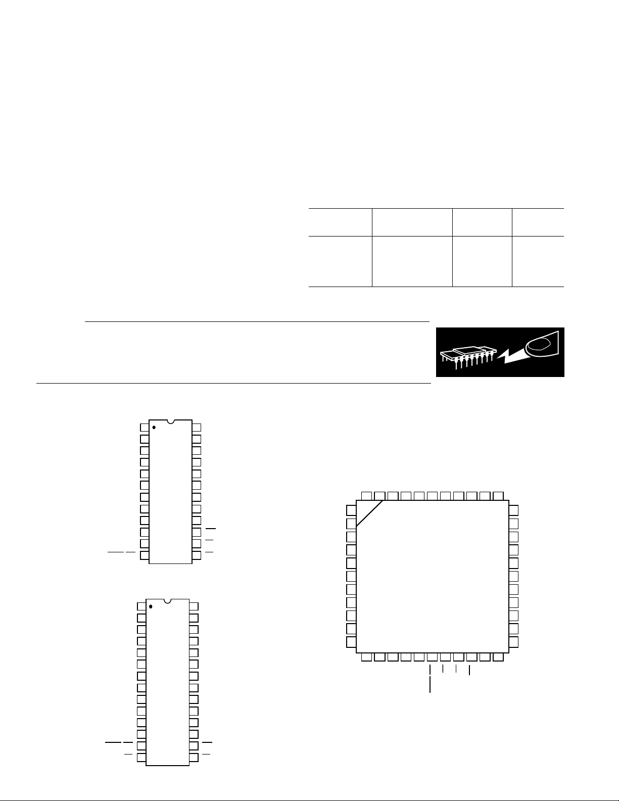
24-Lead SOIC
DB0
DB1
DB2
DB3
DGND
DB4
DB5
DB6
DB7
DB8
(MSB) DB9
BUSY/INT
1
2
3
4
5
AD7776
6
TOP VIEW
7
(Not to Scale)
8
9
10
11
12
24
23
22
20
19
18
17
16
15
14
13
28-Lead PDIP and SOIC
DB0
DB1
NC
DB2
DB3
DGND
DB4
DB5
DB6
DB7
DB8
(MSB) DB9
BUSY/INT
RD
1
2
3
4
5
6
7
AD7777
TOP VIEW
8
(Not to Scale)
9
10
11
12
13
14
NC = NO CONNECT
28
27
26
25
24
23
22
21
20
19
18
17
16
15
21
C
REFIN
AGND
RTN
REFIN
A
IN
AGND
REFOUT
V
CC
CLKIN
WR
CS
RD
C
REFIN
AGND
RTN
REFIN
AIN4
3
A
IN
2
A
IN
1
A
IN
AGND
REFOUT
V
CC
CLKIN
WR
CS
PIN CONFIGURATIONS
1 33
NC
2
NC
3
DB2
4
DB3
5
DGND
6
DB4
7
DB5
8
DB6
9
DB7
10
NC
11
NC
–4–
44-Lead PQFP
REFIN
AGND
DB1
DB0
NC
NC
NC
NC
39 38 37 36 35 3444 43 42 41 40
AD7778
TOP VIEW
(Not to Scale)
12
NC
NC
DB8
(MSB) DB9
18 19 20 21 221716151413
NC
BUSY/INT
RTN
C
CS
RD
WR
NC = NO CONNECT
REFIN
CLKIN
NC
NC
32
31
30
29
28
27
26
25
24
23
AIN8
AIN7
AIN6
AIN5
AIN4
AIN3
AIN2
AIN1
AGND
REFOUT
V
CC
REV. A

Mnemonic Description
AD7776/AD7777/AD7778
PIN FUNCTION DESCRIPTION
V
CC
+5 V Power Supply.
AGND Analog Ground.
DGND Digital Ground. Ground reference for digital circuitry.
DB0–DB9 Input/Output Data Bus. This is a bidirectional data port from which ADC output data may be read and to which
control register data may be written.
BUSY/INT Busy/Interrupt Output. Active low logic output indicating A/D converter status. This logic output has two modes
of operation depending on whether location CR9 of the control register has been set low or high:
If CR9 is set low, the BUSY/INT output behaves as a BUSY signal. The BUSY signal goes low and stays low for the
duration of a single conversion, or if simultaneous sampling has been selected, BUSY stays low for the duration of
both conversions.
If CR9 is set high, BUSY/INT output behaves as an INTERRUPT signal. The INT signal goes low and remains low
after either a single conversion is completed or after a double conversion is completed if simultaneous sampling has
been selected. With CR9 high, the falling edge of WR or RD resets the INT line high.
CS Chip Select Input. The device is selected when this input is low.
WR Write Input (Active Low). It is used in conjunction with CS to write data to the control register. Data is latched to the
registers on the rising edge of WR. Following the rising edge of WR, the analog input is acquired and a conversion is
started.
RD Read Input (Active Low). It is used in conjunction with CS to enable the data outputs from the ADC registers.
A
1–8 Analog Inputs 1–8. The analog input range is V
IN
BIAS
± V
SWING
where V
BIAS
and V
are defined by the reference
SWING
voltage applied to REFIN. Input resistance between any of the analog input pins and AGND is 10 kΩ or greater.
REFIN Voltage Reference Input. The AD7776/AD7777/AD7778 are specified over a voltage reference range of 1.9 V to 2.1 V
with a nominal value of 2.0 V. This REFIN voltage provides the V
V
is equal to REFIN and V
BIAS
is nominally equal to REFIN/2. Input resistance between this REFIN pin and
SWING
BIAS
and V
levels for the input channel(s).
SWING
AGND is 10 kΩ or greater.
REFOUT Voltage Reference Output. This pin provides the internal voltage reference, which is nominally 2.0 V. It can provide
C
REFIN
the bias voltage (V
Reference Decoupling Capacitor. A 10 nF capacitor must be connected from this pin to AGND to ensure correct
) for the input channel(s).
BIAS
operation of the high speed ADC.
RTN Signal Return Path for the input channel(s). Normally RTN is connected to AGND at the package.
CIRCUIT DESCRIPTION
ADC Transfer Function
For all versions, an input signal of the form V
expected. This V
signal level operates as a pseudo ground to
BIAS
which all input signals must be referred. The V
BIAS
± V
BIAS
is
SWING
level is
determined by the voltage applied to the REFIN pin. This can
be driven by an external voltage source or, alternatively, by the
onboard 2 V reference, available at REFOUT. The magnitude
of the input signal swing is equal to V
/2 (or REFIN/2) and is
BIAS
set internally. With a REFIN of 2 V, the analog input signal level
varies from 1 V to 3 V, i.e., 2 ± 1 V. Figure 5 shows the transfer
function of the ADC and its relationship to V
BIAS
and V
SWING
.
The half-scale two's complement code of the ADC, 000 Hex (00
0000 0000 Binary), occurs at an input voltage equal to V
input full-scale range of the ADC is equal to 2 V
SWING
. The
BIAS
, so that the
Plus Full-Scale transition (1FE to 1FF) occurs at a voltage equal to
V
+ V
BIAS
tion (200 to 201) occurs at a voltage V
REV. A
– 1.5 LSBs, and the minus full-scale code transi-
SWING
BIAS
– V
SWING
+ 0.5 LSBs.
–5–
1FF
1FE
ADC
OUTPUT
CODE
(HEX)
000
202
201
200
V
V
BIAS
BIAS–VSWING
ANALOG INPUT, V
IN
Figure 5. ADC Transfer Function
V
BIAS+VSWING

AD7776/AD7777/AD7778
CONTROL REGISTER
The control register is 10-bit wide and can only be written to.
On power-on, all locations in the control register are automatically loaded with 0s. For the single channel AD7776, locations
CR0 to CR6 of the control register are “don’t cares.” For the
quad channel AD7777, locations CR2 and CR5 are “don’t
cares.” Individual bit functions are described below.
CR0–CR2: Channel Address Locations. Determines which channel
is selected and converted for single-channel operation. For simultaneous sampling operation, CR0–CR2 holds the address of one of
the two channels to be sampled.
AD7776
CR2 CR1 CR0 Function
X* XXSelect AIN1
*X = Don’t Care
AD7777
CR2 CR1 CR0 Function
X* 00Select A
X0 1 Select A
X1 0 Select A
X1 1 Select A
*X = Don’t Care
1
IN
2
IN
3
IN
4
IN
AD7778
CR2 CR1 CR0 Function
00 0 Select A
00 1 Select A
01 0 Select A
01 1 Select A
10 0 Select A
10 1 Select A
11 0 Select A
11 1 Select A
1
IN
2
IN
3
IN
4
IN
5
IN
6
IN
7
IN
8
IN
CR3–CR5: Channel Address Locations. Only applicable for simultaneous sampling with the AD7777 or AD7778 when CR3–CR5
holds the address of the second channel to be sampled.
AD7777
CR5 CR4 CR3 Function
X* 00Select A
X0 1 Select A
X1 0 Select A
X1 1 Select A
*X = Don’t Care
1
IN
2
IN
3
IN
4
IN
AD7778
CR5 CR4 CR3 Function
00 0 Select A
00 1 Select A
01 0 Select A
01 1 Select A
10 0 Select A
10 1 Select A
11 0 Select A
11 1 Select A
1
IN
2
IN
3
IN
4
IN
5
IN
6
IN
7
IN
8
IN
CR6: Determines whether operation is on a single channel or
simultaneous sampling on two channels. Location CR6 is a
“don’t care” for the AD7776.
CR6 Function
0 Single channel operation. Channel select
address is contained in locations CR0–CR2.
1 Two channels simultaneously sampled
and sequentially converted. Channel
select addresses contained in locations
CR0–CR2 and CR3–CR5.
CR7: Determines whether the device is in the normal operating
mode or in the half-scale test mode.
CR7 Function
0Normal Operating Mode
1Half-Scale Test Mode
In the half-scale test mode, REFIN is internally connected as an
analog input(s). In this mode, locations CR0–CR2 and CR3–CR5
are all “don’t cares” since it is REFIN which is converted. For
the AD7777 and AD7778, the contents of location CR6 still
determine whether a single or a double conversion is carried out
on the REFIN level.
CR8: Determines whether the device is in the normal operating
mode or in the power-down mode.
CR8 Function
0Normal Operating Mode
1 Power-Down Mode
In the power-down mode all linear circuitry is turned off and the
REFOUT output is weakly (5 kΩ) pulled to AGND. The input
impedance of the analog inputs and of the REFIN input remains
the same in either normal mode or power-down mode. See
under Circuit Description—Power-Down Mode.
CR9: Determines whether BUSY/INT output flag goes low and
remains low during conversion(s) or else goes low and remains
low after the conversion(s) is (are) complete.
CR9 BUSY/INT Functionality
0 Output goes low and remains low during
conversion(s).
1 Output goes low and remains low after conversion(s)
is (are) complete.
–6–
REV. A

AD7776/AD7777/AD7778
ADC Conversion Start Timing
Figure 6 shows the operating waveforms for the start of a conversion cycle. On the rising edge of WR, the conversion cycle starts
with the acquisition and tracking of the selected ADC channel,
A
1–8. The analog input voltage is held 40 ns (typically) after
IN
the first rising edge of CLKIN following four complete CLKIN
cycles. If t
CLKIN as shown is seen as the first falling clock edge. If t
in Figure 6 is greater than 12 ns, the falling edge of
D
is
D
less than 12 ns, the first falling clock edge to be recognized does
not occur until one cycle later.
Following the “hold” on the analog input(s), two complete
CLKIN cycles are allowed for settling purposes before the MSB
decision is made. The actual decision point occurs approximately
40 ns after the rising edge of CLKIN as shown in Figure 6. Two
more CLKIN cycles are allowed for the second MSB decision.
The succeeding bit decisions are made approximately 40 ns
after each rising edge of CLKIN until the conversion is complete.
At the end of conversion, if a single conversion has been
requested (CR6 = 0), the BUSY/INT line changes state (as
programmed by CR9) and the SAR contents are transferred to
the first register ADCREG1. The SAR is then reset in readiness for
a new conversion. If simultaneous sampling has been requested
(CR6 = 1), no change occurs in the status of the BUSY/INT
output, and the ADC automatically starts the second conversion.
At the end of this conversion, the BUSY/INT line changes state
(as programmed by CR9) and the SAR contents are transferred
to the second register, ADCREG2.
WR
tD*
CLKIN
40ns
V
IN
CHANNEL ACQUISITION
*
TIMING SHOWN FOR tD GREATER THAN 12ns
TYP
40ns
TYP
'HOLD' DB9 (MSB)
Figure 6. ADC Conversion Start Timing
Track-and-Hold
The track-and-hold (T/H) amplifiers on the analog input(s) of
the AD7776/AD7777/AD7778 allow the ADC to accurately
convert an input sine wave of 2 V peak-peak amplitude up to a
frequency of 189 kHz, the Nyquist frequency of the ADC when
operated at its maximum throughput rate of 378 kHz. This
maximum rate of conversion includes conversion time and the
time between conversions. Because the input bandwidth of the
track-and-hold is much greater than 189 kHz, the input signal
should be band limited to avoid folding unwanted signals into
the band of interest.
Power-Down
The AD7776/AD7777/AD7778 can be placed in a power-down
mode simply by writing a logic high to location CR8 of the
control register. The following changes are effected immediately
upon writing a “1” to location CR8:
• Any conversion in progress is terminated.
• If a conversion is in progress, the leading edge of WR immedi-
ately drives the BUSY/INT output high.
• All the linear circuitry is turned off.
• The REFOUT output stops being driven and is weakly (5 kΩ)
pulled to analog ground.
Control inputs CS, WR, and RD retain their purpose while the
AD7776/AD7777/AD7778 is in power-down mode. If no
conversions are in progress when the AD7776/AD7777/AD7778
is placed into power-down mode, the contents of the ADC
registers, ADCREG1 and ADCREG2, are retained during
power-down and can be read as normal. On returning to normal
operating mode, a new conversion (or conversions, dependent
on CR6) is automatically started. Upon completion, the invalid
conversion results are loaded into the ADC registers, losing the
previous valid results.
To achieve the lowest possible power consumption in the
power-down mode, special attention must be paid to the state of
the digital and analog inputs and outputs:
• Because each analog input channel sees a resistive divider to
AGND, the input resistance of which does not change
between normal and power-down modes, driving the analog
input signals to 0 V or as close as possible to 0 V minimizes
the power dissipated in the input signal conditioning circuitry.
• Similarly, the REFIN input sees a resistive divider to AGND,
the input resistance of which does not change between
normal and power-down modes. If an external reference is
being used, then driving this reference input to 0 V or as
close as possible to 0 V minimizes the power dissipated in
the input signal conditioning circuitry.
• Since the REFOUT pin is pulled to AGND via, typically, a
5 kΩ resistor, any voltage above 0 V that this output may be
pulled to by external circuitry dissipates unnecessary power.
• Digital inputs CS, WR, and RD should all be held at V
CC
or
as close as possible. CLKIN should be held as close as
possible to either 0 V or V
CC.
• Since the BUSY/INT output is actively driven to a logic high,
any loading on this pin to 0 V dissipates power.
The AD7776/AD7777/AD7778 comes out of the power-down
mode when a Logic “0” is written to location CR8 of the
control register. Note that the contents of the other locations
in the control register are retained when the device is placed in
power-down and are valid when power is restored. However,
coming out of power-down provides an opportunity to reload
the complete contents of the control register without any
extra instructions.
REV. A
–7–

AD7776/AD7777/AD7778
Microprocessor Interfacing Circuits
The AD7776/AD7777/AD7778 family of ADCs is intended to
interface to DSP machines such as the ADSP-2101, ADSP-2105,
the TMS320 family and microcontrollers such as the 80C196
family.
Figure 7 shows the AD7776/AD7777/AD7778 interfaced to the
TMS320C10 at 20.5 MHz and the TMS320C14 at 25 MHz.
Figure 8 shows the interface with the TMS320C25 at 40 MHz.
Note that one wait state is required with this interface. The
ADSP-2101-50 and the ADSP-2105-40 interface is shown in
Figure 9. One wait state is required with these machines.
A11–A0
TMS320C10-20.5
TMS320C14-25
(C10) DEN
(C14) REN
D15–D0
WE
ADDRESS BUS
ADDR
DECODE
CS
AD7776/
AD7777/
AD7778
WR
RD
DB9–DB0
DATA BUS
*
ADDITIONAL PINS OMITTED FOR CLARITY
*
Figure 10 shows the interface with the 80C196KB at 12 MHz
and the 80C196KC at 16 MHz. One wait state is required with
the 16 MHz machine. The 80C196 is configured to operate
with a 16-bit multiplexed address/data bus.
Table I provides a truth table for the AD7776/AD7777/AD7778
and summarizes their microprocessor interfacing features. Note
that a read instruction to any of the devices while a conversion
is in progress immediately stops that conversion and returns
unreliable data over the data bus.
ADSP-2101-50
ADSP-2105-40
A13–A0
DMS
WR
RD
D23–D6
ADDRESS BUS
ADDR
DECODE
EN
DATA BUS
*ADDITIONAL PINS OMITTED FOR CLARITY
CS
AD7776/
AD7777/
AD7778
WR
RD
DB9–DB0
*
Figure 7. AD7776/AD7777/AD7778 to TMS320C10 and
TMS320C14 Interface
A15–A0
IS
READY
MSC
STRB
R/W
TMS320C25-40
D15–D0
ADDRESS BUS
ADDR
DECODE
CS
AD7776/
AD7777/
AD7778
WR
RD
DB9–DB0
DATA BUS
*
ADDITIONAL PINS OMITTED FOR CLARITY
*
Figure 8. AD7776/AD7777/AD7778 to TMS320C25 Interface
Figure 9. AD7776/AD7777/AD7778 to ADSP-2101 and
ADSP-2105 Interface
AD15–AD6
(PORT 4)
80C196KB-12
80C196KC-16
AD7–AD0
(PORT 3)
ADDRESS BUS
ALE
WR
RD
*ADDITIONAL PINS OMITTED FOR CLARITY
‘373
LATCH
DATA BUS (10)
ADDR
DECODER
AD7776/
AD7777/
AD7778
CS
WR
RD
DB9–DB0
*
Figure 10. AD7776/AD7777/AD7778 to 80C196 Interface
–8–
REV. A

AD7776/AD7777/AD7778
Table I. AD7776/AD7777/AD7778 Truth Table for Microprocessor Interfacing
CS RD WR DB0–DB9 Function/Comments
1X* X* High Z Data Port High Impedance
01 j CR Data Load control register (CR) data to control register and start a conversion.
0 k 1 ADC Data ADC data placed on data bus. Depending upon location CR6 of the control register, one or two
Read instructions are required.
If CR6 is low, i.e., single-channel conversion selected, a read instruction returns the contents of
ADCREG1. Succeeding read instructions continue to return the contents of ADCREG1.
If CR6 is high, i.e., simultaneous sampling (double conversion) selected, the first read instruction
returns the contents of ADCREG1 while the second read instruction returns the contents of
ADCREG2. A third read instruction returns ADCREG1 again, the fourth ADCREG2, etc.
*X = Don’t Care
DESIGN INFORMATION
Layout Hints
Ensure that the layout for the printed circuit board has the digital and analog grounds separated as much as possible. Take care
not to run any digital track alongside an analog signal track.
Guard (screen) the analog input(s) with RTN.
Establish a single-point analog ground separate from the logic
system ground and as close as possible to the AD7776/AD7777/
AD7778. Both the RTN and AGND pins on the AD7776/
AD7777/AD7778 and all other signal grounds should be connected to this single point analog ground. In turn, this star
ground should be connected to the digital ground at one point
only—preferably at the low impedance power supply itself.
Low impedance analog and digital power supply common returns
are important for correct operation of the devices, so make the
foil width for these tracks as wide as possible.
To ensure a low impedance +5 V power supply at the actual V
CC
pin, it is necessary to use bypass capacitors from the pin itself to
DGND. A 4.7 µF tantalum capacitor in parallel with a 0.1 µF
ceramic capacitor is sufficient.
ADC Corruption
Executing a read instruction to the AD7776/AD7777/AD7778
while a conversion is in progress immediately halts the conversion
and returns invalid data over the data bus. The BUSY/ INT
output pin should be monitored closely and all read instructions
to the AD7776/AD7777/AD7778 prevented while this output
shows that a conversion is in progress.
Executing a write instruction to the AD7776/AD7777/AD7778
while a conversion is in progress immediately halts the conversion,
while the falling edge of WR driving the BUSY/INT output high.
The analog input(s) is sampled as normal, and a new conversion
sequence (dependent upon CR6) is started.
ADC Conversion Time
Although each conversion takes only 14 CLKIN cycles, it can take
between 4.5 and 5.5 CLKIN cycles to acquire the analog input(s)
after the WR input goes high and before any conversions start.
TERMINOLOGY
Relative Accuracy
For the AD7776/AD7777/AD7778, relative accuracy or endpoint
nonlinearity is the maximum deviation, in LSBs, of the ADC’s
actual code transition points from a straight line drawn between
the endpoints of the ADC transfer function.
Differential Nonlinearity
Differential nonlinearity is the difference between the measured
change and the ideal 1 LSB change between any two adjacent
codes. A specified maximum differential nonlinearity of ±1 LSB
ensures no missed codes.
Bias Offset Error
For an ideal 10-bit ADC, the output code for an input voltage
equal to V
should be midscale. The bias offset error is the
BIAS
difference between the actual midpoint voltage for midscale code
and V
Bias Offset Error Match
, expressed in LSBs.
BIAS
This is a measure of how closely the bias offset errors of all
channels track each other. The bias offset error match of any
channel must be no further away than 10 LSBs from the bias
offset error of any other channel, regardless of whether the
channels are independently sampled or simultaneously sampled.
Plus and Minus Full-Scale Error
The input channels of the ADC can be considered to have
bipolar (positive and negative) input ranges, but are referred to
V
(or REFIN) instead of AGND. Positive full-scale error for
BIAS
the ADC is the difference between the actual input voltage
required to produce the plus full-scale code transition and the ideal
input voltage (V
BIAS
+ V
–1.5 LSB), expressed in LSBs.
SWING
Minus full-scale error is similarly specified for the minus full-scale
code transition, relative to the ideal input voltage for this
transition (V
BIAS
– V
+ 0.5 LSB). Note that the full-scale
SWING
errors for the ADC input channels are measured after their
respective bias offset errors have been adjusted out.
Plus and Minus Full-Scale Error Match
This is a measure of how closely the full-scale errors of all
channels track each other. The full-scale error match of any channel
must be no further away than 10 LSBs from the respective
full-scale error of any other channel, regardless of whether the
channels are independently sampled or simultaneously sampled.
REV. A
–9–
AD7776/AD7777/AD7778
Short Circuit Current
This is defined as the maximum current which flows either
into or out of the REFOUT pin if this pin is shorted to any
potential between 0 V and V
. This condition can be allowed
CC
for up to 10 seconds provided that the power dissipation of the
package is not exceeded.
Signal-to-Noise and Distortion Ratio, S/(N+D)
Signal-to-noise and distortion ratio, S/(N+D), is the ratio of the
rms value of the measured input signal to the rms sum of all
other spectral components below the Nyquist frequency, including harmonics, but excluding dc. The value for S/(N+D) is
given in decibels.
Total Harmonic Distortion, THD
Total harmonic distortion is the ratio of the rms sum of the first
five harmonic components to the rms value of a full-scale input
signal and is expressed in decibels. For the AD7776/AD7777/
AD7778, total harmonic distortion (THD) is defined as:
2
2
2
VVVVV
++++
()
2
20
log
3
2
4
5
V
1
12
2
6
where V1 is the rms amplitude of the fundamental and V2,
V
, V4, V5, and V6 are the rms amplitudes of the individual
3
harmonics.
Intermodulation Distortion, IMD
With inputs consisting of sine waves at two frequencies, fa and fb,
any active device with nonlinearities creates distortion products,
of order (m + n), at sum and difference frequencies of mfa + nfb,
where m, n = 0, 1, 2, 3. Intermodulation terms are those for which
m or n is not equal to zero. For example, the second order terms
include (fa + fb) and (fa – fb) and the third order terms include
(2 fa + fb), (2 fa – fb), (fa + 2 fb), and (fa – 2 fb).
Channel-to-Channel Isolation
Channel-to-channel isolation is a measure of the level of cross-talk
between channels. It is measured by applying a full-scale 100 kHz
sine wave signal to any one of the input channels and monitoring
the remaining channels. The figure given is the worst case across
all channels.
DIGITAL SIGNAL PROCESSING APPLICATIONS
In digital signal processing (DSP) application areas like voice
recognition, echo cancellation, and adaptive filtering, the dynamic
characteristics S/(N+D), THD, and IMD of the ADC are critical.
The AD7776/AD7777/AD7778 are specified dynamically as well
as with standard dc specifications. Because the track/hold
amplifier has a wide bandwidth, an antialiasing filter should be
placed on the analog inputs to avoid aliasing high frequency noise
back into the bands of interest.
The dynamic performance of the ADC is evaluated by applying a
sine wave signal of very low distortion to a single analog input
which is sampled at 380.95 kHz. A fast Fourier transform (FFT)
plot or histogram plot is then generated from which the signal to
noise and distortion, harmonic distortion, and dynamic differential
nonlinearity data can be obtained. Similarly, for intermodulation
distortion, an input signal consisting of two pure sine waves at
different frequencies is applied to the AD7776/AD7777/AD7778.
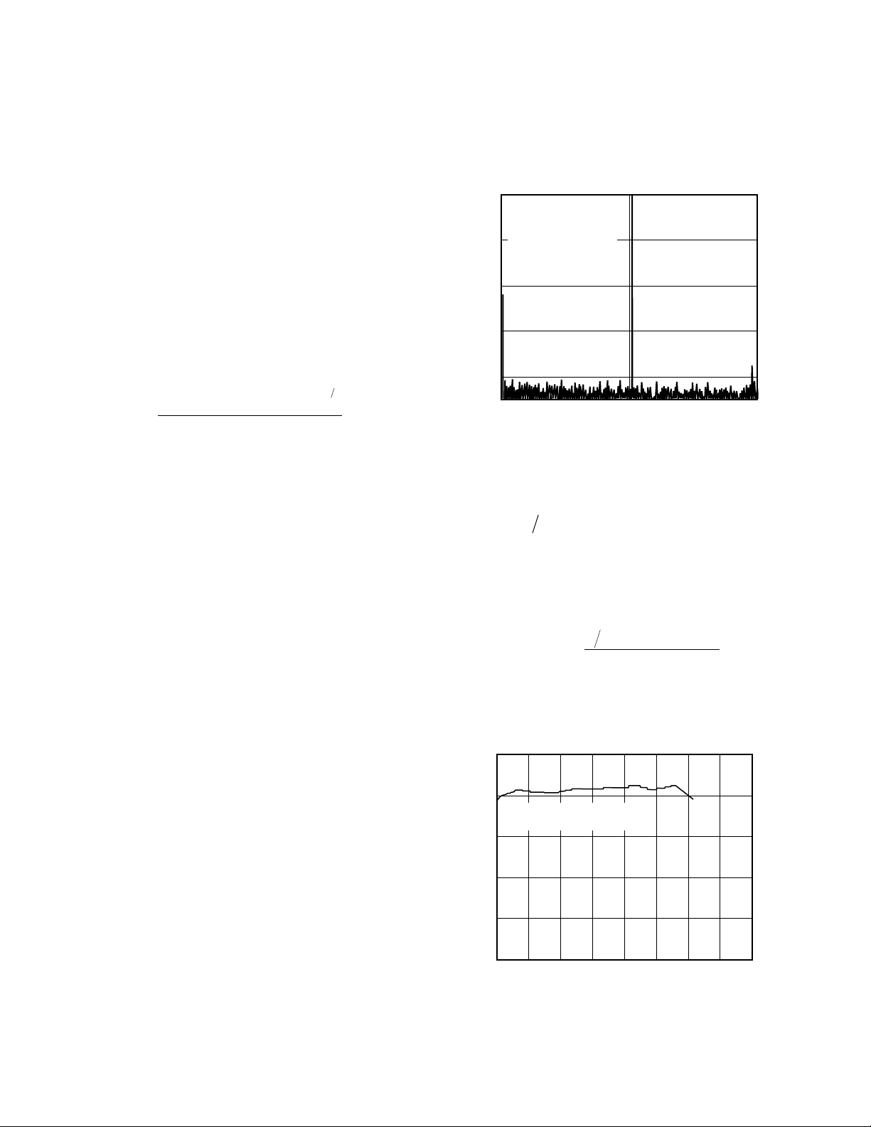
Figure 11 shows a 2048-point FFT plot for a single channel of
the AD7778 with an input signal of 99.88 kHz. The SNR is
58.71 dB. It can be seen that most of the harmonics are buried
in the noise floor. It should be noted that the harmonics are
taken into account when calculating the S/(N+D).
0
INPUT FREQUENCY =
99.88kHz
SAMPLE FREQUENCY =
380.95kHz
–20
SNR
= 58.7dB
= 25ⴗC
T
A
–40
–60
SIGNAL AMPLITUDE – dB
–80
–90
0
99.88
FREQUENCY – kHz
Figure 11. ADC FFT Plot
The relationship between S/(N+D) and resolution (n) is expressed by the following equation:
SN D n dB+
()
=+
602 176..
()
This is for an ideal part with no differential or integral linearity
errors. These errors cause a degradation in S/(N+D). By working backwards from the above equation, it is possible to get a
measure of ADC performance expressed in effective number
of bits (n).
SN DdB
+
n effective
()
()()
=
602..
− 176
The effective number of bits plotted versus frequency for a
single channel of the AD7778 is shown in Figure 12. The effective number of bits is typically 9.5.
10.0
9.5
SAMPLE FREQUENCY = 378.4kHz
= 24ⴗC
T
A
9.0
8.5
8.0
EFFECTIVE NUMBER OF BITS
7.5
0
INPUT FREQUENCY – kHz
189.2
Figure 12. Effective Number of Bits vs. Frequency
–10–
REV. A

AD7776/AD7777/AD7778
Changing the Analog Input Voltage Range
By biasing the RTN pin above AGND, it is possible to change
the analog input voltage range from its V
a more traditional 0 V to V
range. The new input range can
REF
BIAS
± V
SWING
format to
be described as
where 0 V ≤ V
VtoV REFIN
OFFSET OFFSET
OFFSET
()
≤ 1 V. To produce this range, the RTN pin
must be biased to (REFIN – 2 V
+
). For instance, if
OFFSET
OUTLINE DIMENSIONS
24-Lead Standard Small Outline Package [SOIC]
Wide Body
(RW-24)
Dimensions shown in millimeters and (inches)
15.60 (0.6142)
15.20 (0.5984)
24 13
1
0.30 (0.0118)
0.10 (0.0039)
COPLANARITY
0.10
1.27 (0.0500)
BSC
CONTROLLING DIMENSIONS ARE IN MILLIMETERS; INCH DIMENSIONS
(IN PARENTHESES) ARE ROUNDED-OFF MILLIMETER EQUIVALENTS FOR
REFERENCE ONLY AND ARE NOT APPROPRIATE FOR USE IN DESIGN
COMPLIANT TO JEDEC STANDARDS MS-013AD
0.51 (0.020)
0.33 (0.013)
RTN is tied to REFOUT, then the analog input range becomes
0 V to 2 V. The fixed 2 V analog input voltage span of the ADC
can range from 1 V to 3 V (RTN = 0 V) to 0 V to 2 V (RTN =
2 V), i.e., with proper biasing, an input signal range from 0.3 V
to 2.3 V can be covered. Both the relative accuracy and differential nonlinearity performance remain essentially unchanged in
this mode, while the SNR and THD performance are typically
2 dB to 3 dB worse than standard.
7.60 (0.2992)
7.40 (0.2913)
12
2.65 (0.1043)
2.35 (0.0925)
SEATING
PLANE
10.65 (0.4193)
10.00 (0.3937)
0.32 (0.0126)
0.23 (0.0091)
0.75 (0.0295)
0.25 (0.0098)
8ⴗ
0ⴗ
ⴛ 45ⴗ
1.27 (0.0500)
0.40 (0.0157)
28-Lead Standard Small Outline Package [SOIC]
Wide Body
(RW-28)
Dimensions shown in millimeters and (inches)
18.10 (0.7126)
17.70 (0.6969)
28 15
1
0.30 (0.0118)
0.10 (0.0039)
COPLANARITY
0.10
CONTROLLING DIMENSIONS ARE IN MILLIMETERS; INCH DIMENSIONS
(IN PARENTHESES) ARE ROUNDED-OFF MILLIMETER EQUIVALENTS FOR
REFERENCE ONLY AND ARE NOT APPROPRIATE FOR USE IN DESIGN
1.27 (0.0500)
COMPLIANT TO JEDEC STANDARDS MS-013AE
BSC
0.51 (0.0201)
0.33 (0.0130)
14
2.65 (0.1043)
2.35 (0.0925)
SEATING
PLANE
7.60 (0.2992)
7.40 (0.2913)
0.32 (0.0126)
0.23 (0.0091)
10.65 (0.4193)
10.00 (0.3937)
0.75 (0.0295)
0.25 (0.0098)
8ⴗ
0ⴗ
ⴛ 45ⴗ
1.27 (0.0500)
0.40 (0.0157)
REV. A
–11–

AD7776/AD7777/AD7778
6.35
(0.2500)
MAX
5.05 (0.1988)
3.18 (0.1252)
OUTLINE DIMENSIONS
28-Lead Plastic Dual-in-Line Package [PDIP]
(N-28)
Dimensions shown in millimeters and (inches)
39.70 (1.5630)
35.10 (1.3819)
28
1
0.56 (0.0220)
0.36 (0.0142)
CONTROLLING DIMENSIONS ARE IN MILLIMETERS; INCH DIMENSIONS
(IN PARENTHESES) ARE ROUNDED-OFF MILLIMETER EQUIVALENTS FOR
REFERENCE ONLY AND ARE NOT APPROPRIATE FOR USE IN DESIGN
2.54
(0.1000)
BSC
1.77
(0.0697)
MAX
15
14.73 (0.5799)
12.32 (0.4850)
14
1.52 (0.0598)
0.38 (0.0150)
3.81
(0.1500)
MIN
SEATING
PLANE
15.87 (0.6248)
15.24 (0.6000)
0.38 (0.0150)
0.20 (0.0079)
44-Lead Plastic Quad Flatpack [PQFP]
(S-44)
Dimensions shown in millimeters
4.95 (0.1949)
3.18 (0.1252 )
C01196–0–10/02(A)
33
1
0.80
BSC
13.20 BSC SQ
10.00 BSC SQ
TOP VIEW
(PINS DOWN)
PIN 1
23
22
12
11
0.45
0.29
1.03
0.88
0.73
SEATING
PLANE
COPLANARITY
0.10
0.25 MAX
2.45
MAX
8ⴗ
0.8ⴗ
34
44
2.20
2.00
1.80
COMPLIANT TO JEDEC STANDARDS MS-022-AB
Revision History
Location Page
10/02—Data Sheet changed from REV. 0 to REV. A.
Changes to SPECIFICATIONS . . . . . . . . . . . . . . . . . . . . . . . . . . . . . . . . . . . . . . . . . . . . . . . . . . . . . . . . . . . . . . . . . . . . . . . . . . . . 2
Changes to ORDERING GUIDE . . . . . . . . . . . . . . . . . . . . . . . . . . . . . . . . . . . . . . . . . . . . . . . . . . . . . . . . . . . . . . . . . . . . . . . . . . . 4
Changes to Total Harmonic Distortion, THD section . . . . . . . . . . . . . . . . . . . . . . . . . . . . . . . . . . . . . . . . . . . . . . . . . . . . . . . . . . . 10
Changes to OUTLINE DIMENSIONS . . . . . . . . . . . . . . . . . . . . . . . . . . . . . . . . . . . . . . . . . . . . . . . . . . . . . . . . . . . . . . . . . . . . . 12
PRINTED IN U.S.A.
–12–
REV. A

 Loading...