Analog Devices AD7777AS, AD7777AR, AD7776AR, AD7776AN Datasheet

REV. 0
Information furnished by Analog Devices is believed to be accurate and
reliable. However, no responsibility is assumed by Analog Devices for its
use, nor for any infringements of patents or other rights of third parties
which may result from its use. No license is granted by implication or
otherwise under any patent or patent rights of Analog Devices.
a
LC2MOS, High Speed
1-, 4- & 8-Channel 10-Bit ADCs
AD7776/AD7777/AD7778*
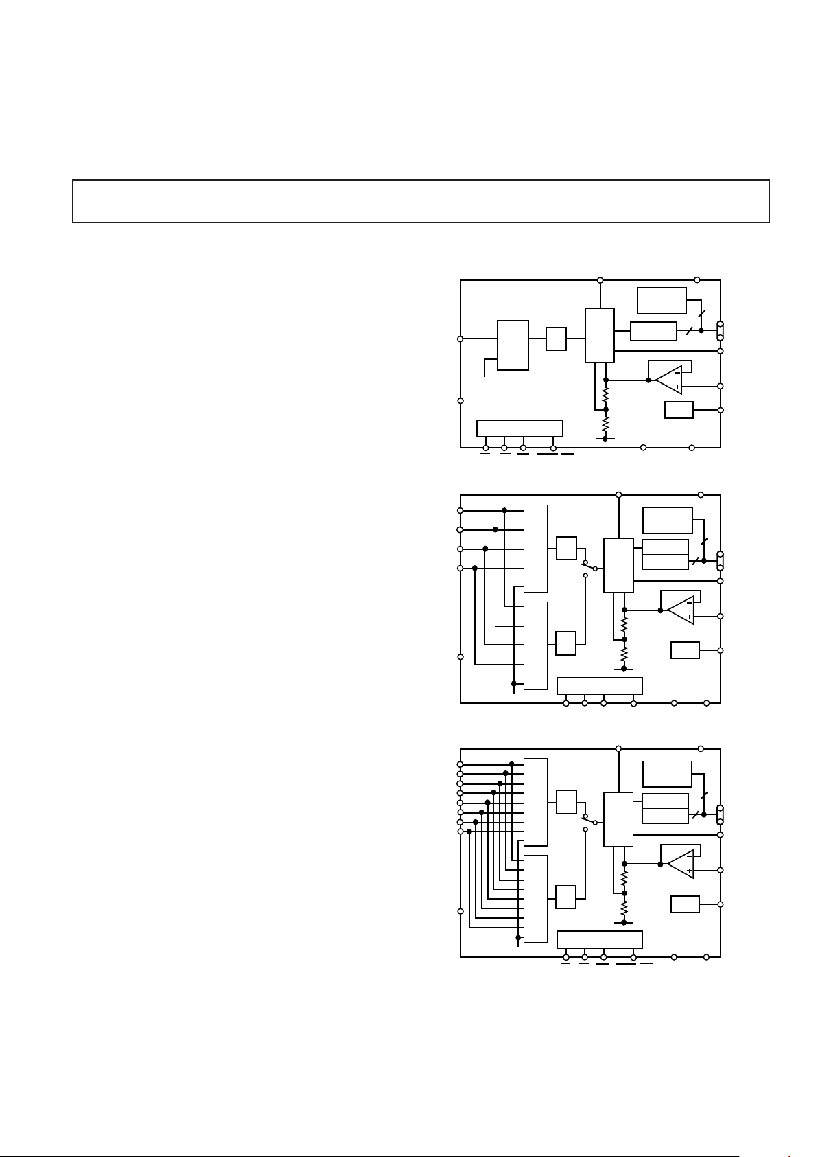
FUNCTIONAL BLOCK DIAGRAMS
CS RD WR
BUSY/INT
AGND
DB0–DB9
AD7776
10
DGND
CLKIN
10
CONTROL
REGISTER
ADCREG1
T/H
REFOUT
REFIN
REF
AGND
C
REFIN
RTN
V
SWING
V
BIAS
AIN1
MUX
REFIN
10-BIT
ADC
CONTROL LOGIC
V
CC
AGND
DB0–DB9
AD7777
10
CONTROL
REGISTER
DGND
CLKIN
10
ADCREG2
ADCREG1
T/H
1
REFOUT
REFIN
REF
AGND
C
REFIN
V
SWING
V
BIAS
AIN1
AIN2
AIN3
AIN4
MUX
1
REFIN
T/H
2
MUX
2
10-BIT
ADC
CONTROL LOGIC
V
CC
RTN
AGND
DB0–DB9
AD7778
10
CONTROL
REGISTER
DGND
CLKIN
CSRDWR
BUSY/INT
10
ADCREG2
ADCREG1
T/H
1
REFOUT
REFIN
REF
AGND
C
REFIN
V
SWING
V
BIAS
AIN1
A
IN
2
A
IN
3
A
IN
4
A
IN
5
A
IN
6
A
IN
7
A
IN
8
MUX
1
REFIN
T/H
2
MUX
2
10-BIT
ADC
CONTROL LOGIC
V
CC
RTN
FEATURES
AD7776: Single Channel
AD7777: 4-Channel
AD7778: 8-Channel
Fast 10-Bit ADC: 2.5 ms Worst Case
+5 V Only
Half-Scale Conversion Option
Fast Interface Port
Power-Down Mode
APPLICATIONS
HDD Servos
Instrumentation
GENERAL DESCRIPTION
The AD7776, AD7777 and AD7778 are a family of high speed,
multichannel, 10-bit ADCs primarily intended for use in R/W
head positioning servos found in high density hard disk drives.
They have unique input signal conditioning features that make
them ideal for use in such single supply applications.
By setting a bit in a control register within both the four-channel
version, AD7777, and the eight-channel version, AD7778, the
input channels can either be independently sampled or any two
channels of choice can be simultaneously sampled. For all versions the specified input signal range is of the form V
BIAS
±
V
SWING
. However, if the RTN pin is biased at, say, 2 V the
analog input signal range becomes 0 V to +2 V for all input
channels. This is covered in more detail under the section
Changing the Analog Input Voltage Range. The voltage V
BIAS
is the offset of the ADC’s midpoint code from ground and is
supplied either by an onboard reference available to the user
(REFOUT) or by an external voltage reference applied to
REFIN. The full-scale range (FSR) of the ADC is equal to
2 V
SWING
where V
SWING
is nominally equal to REFIN/2. Additionally, when placed in the half-scale conversion mode, the
value of REFIN is converted. This allows the channel offset(s)
to be measured.
Control register loading and ADC register reading, channel select and conversion start are under the control of the µP. The
twos complemented coded ADCs are easily interfaced to a standard 16-bit MPU bus via their 10-bit data port and standard
microprocessor control lines.
The AD7776/AD7777/AD7778 are fabricated in linear compatible CMOS (LC
2
MOS), an advanced, mixed technology process
that combines precision bipolar circuits with low power CMOS
logic. The AD7776 is available in a 24-pin SOIC package; the
AD7777 is available in both 28-pin DIP and 28-pin SOIC packages; the AD7778 is available in a 44-pin PQFP package.
*Protected by U.S. Patent No. 4,990,916.
One Technology Way, P.O. Box 9106, Norwood, MA 02062-9106, U.S.A.
Tel: 617/329-4700 World Wide Web Site: http://www.analog.com
Fax: 617/326-8703 © Analog Devices, Inc., 1997

REV. 0
–2–
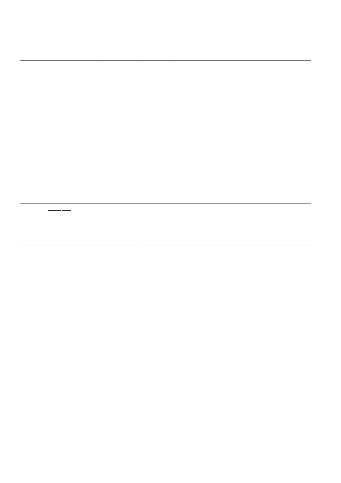
AD7776/AD7777/AD7778–SPECIFICATIONS
(VCC = +5 V 6 5%; AGND = DGND = O V;
CLKIN = 8 MHz; RTN = O V; C
REFIN
= 10 nF; all specifications T
MIN
to T
MAX
unless otherwise noted.)
Parameter A Versions
1
Units Conditions/Comments
DC ACCURACY
Resolution
2
10 Bits
Relative Accuracy ±1 LSB max See Terminology
Differential Nonlinearity ±1 LSB max No Missing Codes; See Terminology
Bias Offset Error ±12 LSB max See Terminology
Bias Offset Error Match 10 LSB max Between Channels, AD7777/AD7778 Only; See Terminology
Plus or Minus Full-Scale Error ±12 LSB max See Terminology
Plus or Minus Full-Scale Error Match 10 LSB max Between Channels, AD7777/AD7778 Only; See Terminology
ANALOG INPUTS
Input Voltage Range
All Inputs V
BIAS
± V
SWING
V min/V max
Input Current +200 µA max VIN = V
BIAS
± V
SWING
; Any Channel
REFERENCE INPUT
REFIN 1.9/2.1 V min/V max For Specified Performance
REFIN Input Current +200 µA max
REFERENCE OUTPUT
REFOUT 1.9/2.1 V min/V max Nominal REFOUT = 2.0 V
DC Output Impedance 5 Ω typ
Reference Load Change ±2 mV max For Reference Load Current Change of 0 to ±500 µA
±5 mV max For Reference Load Current Change of 0 to ±1 mA
Reference Load Should Not Change During Conversion
Short Circuit Current
3
20 mA max See Terminology
LOGIC OUTPUTS
DB0–DB9, BUSY/INT
V
OL
, Output Low Voltage 0.4 V max I
SINK
= 1.6 mA
V
OH
, Output High Voltage 4.0 V min I
SOURCE
= 200 µA
Floating State Leakage Current ±10 µA max
Floating State Capacitance
3
10 pF max
ADC Output Coding Twos Complement
LOGIC INPUTS
DB0–DB9,
CS, WR, RD, CLKIN
Input Low Voltage, V
INL
0.8 V max
Input High Voltage, V
INH
2.4 V min
Input Leakage Current 10 µA max
Input Capacitance
3
10 pF max
CONVERSION TIMING
Acquisition Time 4.5 t
CLKIN
ns min See Terminology
5.5 t
CLKIN
+ 70 ns max
Single Conversion 14 t
CLKIN
ns max
Double Conversion 28 t
CLKIN
ns max
t
CLKIN
125/500 ns min/ns max Period of Input Clock CLKIN
t
CLKIN
High 50 ns min Minimum High Time for CLKIN
t
CLKIN
Low 40 ns min Minimum Low Time for CLKIN
POWER REQUIREMENTS
V
CC
Range +4.75/+5.25 V min/V max For Specified Performance
I
CC
, Normal Mode 15 mA max CS = RD = +5 V, CR8 = 0
I
CC
, Power-Down Mode 1.5 mA max CR8 = 1. All Linear Circuitry OFF
Power-Up Time to Operational
Specifications 500 µs max From Power-Down Mode
DYNAMIC PERFORMANCE See Terminology
Signal to Noise and Distortion
S/(N+D) Ratio –57 dB min V
IN
= 99.88 kHz Full-Scale Sine Wave with f
SAMPLING
= 380.95 kHz
Total Harmonic Distortion (THD) –60 dB min V
IN
= 99.88 kHz Full-Scale Sine Wave with f
SAMPLING
= 380.95 kHz
Intermodulation Distortion (IMD) –75 dB typ fa = 103.2 kHz, fb = 96.5 kHz with f
SAMPLING
= 380.95 kHz. Both
Signals Are Sine Waves at Half-Scale Amplitude
Channel-to-Channel Isolation –90 dB typ VIN = 100 kHz Full-Scale Sine Wave with f
SAMPLING
= 380.95 kHz
NOTES
1
Temperature range as follows: A = –40°C to +85°C.
2
1 LSB = (2 × V
SWING
)/1024 = 1.95 mV for V
SWING
= 1.0 V.
3
Guaranteed by design, not production tested.
Specifications subject to change without notice.

AD7776/AD7777/AD7778
–3–
REV. 0
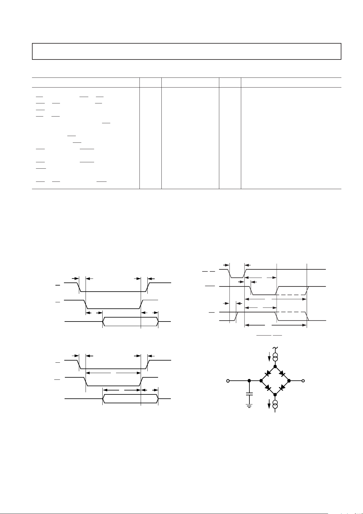
TIMING SPECIFICATIONS
1, 2
(VCC = +5 V 6 5%; AGND = DGND = 0 V; all specifications T
MIN
to T
MAX
unless otherwise noted.)
t
3
t
11
t
10
t
9
t
8
FIRST
CONVERSION
FINISHED
(CR6 = 0)
SECOND
CONVERSION
FINISHED (CR6 = 1)
AD7777/AD7778 ONLY
t
9
BUSY
(CR8 = 0)
INT
(CR8 = 1)
t
10
WR, RD
Figure 3.
BUSY/INT
Timing
I
OL
1.6mA
+2.1V
I
OH
200µA
C
OUT
100pF
DB n
Figure 4. Load Circuit for Bus Timing Characteristics
t
1
CS
t
2
t
4
t
5
RD
DB0–DB9
Figure 1. Read Cycle Timing
t
1
CS
t
2
t
6
WR
DB0–DB9
t
3
t
7
Figure 2. Write Cycle Timing
Parameter Label Limit at T
MIN
to T
MAX
Units Test Conditions/Comments
INTERFACE TIMING
CS Falling Edge to WR or RD Falling Edge t
1
0 ns min
WR or RD Rising Edge to CS Rising Edge t
2
0 ns min
WR Pulse Width t
3
53 ns min
CS or RD Active to Valid Data
3
t
4
60 ns max Timed from Whichever Occurs Last
Bus Relinquish Time after
RD
4
t
5
10 ns min
45 ns max
Data Valid to WR Rising Edge t
6
55 ns min
Data Valid after
WR Rising Edge t
7
10 ns min
WR Rising Edge to BUSY Falling Edge t
8
1.5 t
CLKIN
ns min CR9 = 0
2.5 t
CLKIN
+ 70 ns max
WR Rising Edge to BUSY Rising Edge or
INT Falling Edge t
9
19.5 t
CLKIN
+ 70 ns max Single Conversion, CR6 = 0
t
10
33.5 t
CLKIN
+ 70 ns max Double Conversion, CR6 = 1
WR or RD Falling Edge to INT Rising Edge t
11
60 ns max CR9 = 1
NOTES
1
See Figures 1 to 3.
2
Timing specifications in bold print are 100% production tested. All other times are guaranteed by design, not production tested. All input signals are specified with
tr = tf = 5 ns (10% to 90% of 5 V) and timed from a voltage level of 1.6 V.
3
t4 is measured with the load circuit of Figure 4 and defined as the time required for an output to cross 0.8 V or 2.4 V.
4
t5 is derived from the measured time taken by the data outputs to change 0.5 V when loaded with the circuit of Figure 4. The measured time is then extrapolated back
to remove the effects of charging or discharging the 100 pF capacitor. This means that the time t5 quoted above is the true bus relinquish time of the device and, as
such, is independent of the external bus loading capacitance.
Specifications subject to change without notice.

AD7776/AD7777/AD7778
–4–
REV. 0
ABSOLUTE MAXIMUM RATINGS*
(TA = +25°C unless otherwise noted)
VCC to AGND or DGND . . . . . . . . . . . . . . . . . .–0.3 V, +7 V
AGND, RTN to DGND . . . . . . . . . . . . . –0.3 V, V
CC
+ 0.3 V
CS, RD, WR, CLKIN, DB0–DB9,
BUSY/INT to DGND . . . . . . . . . . . . . –0.3 V, VCC + 0.3 V
Analog Input Voltage to AGND . . . . . . . –0.3 V, V
CC
+ 0.3 V
REFOUT to AGND . . . . . . . . . . . . . . . . –0.3 V, V
CC
+ 0.3 V
REFIN to AGND . . . . . . . . . . . . . . . . . . –0.3 V, V
CC
+ 0.3 V
Operating Temperature Range
All Versions . . . . . . . . . . . . . . . . . . . . . . . . –40°C to +85°C
Storage Temperature Range . . . . . . . . . . . . –65°C to +150°C
Junction Temperature . . . . . . . . . . . . . . . . . . . . . . . . +150°C
DIP Package, Power Dissipation . . . . . . . . . . . . . . . . 875 mW
θ
JA
Thermal Impedance . . . . . . . . . . . . . . . . . . . . . 75°C/W
Lead Temperature, Soldering (10 sec) . . . . . . . . . . +260°C
SOIC Packages, Power Dissipation . . . . . . . . . . . . . . 875 mW
θ
JA
Thermal Impedance . . . . . . . . . . . . . . . . . . . . . 75°C/W
Lead Temperature, Soldering
Vapor Phase (60 sec) . . . . . . . . . . . . . . . . . . . . . . +215°C
Infrared (15 sec) . . . . . . . . . . . . . . . . . . . . . . . . . +220°C
PQFP Package, Power Dissipation . . . . . . . . . . . . . . 500 mW
θ
JA
Thermal Impedance . . . . . . . . . . . . . . . . . . . . . 95°C/W
Lead Temperature, Soldering
Vapor Phase (60 sec) . . . . . . . . . . . . . . . . . . . . . . +215°C
Infrared (15 sec) . . . . . . . . . . . . . . . . . . . . . . . . . +220°C
*Stresses above those listed under “Absolute Maximum Ratings” may cause
permanent damage to the device. This is a stress rating only; functional operation
of the device at these or any other conditions above those listed in the operational
sections of this specification is not implied. Exposure to absolute maximum rating
conditions for extended periods may affect device reliability.
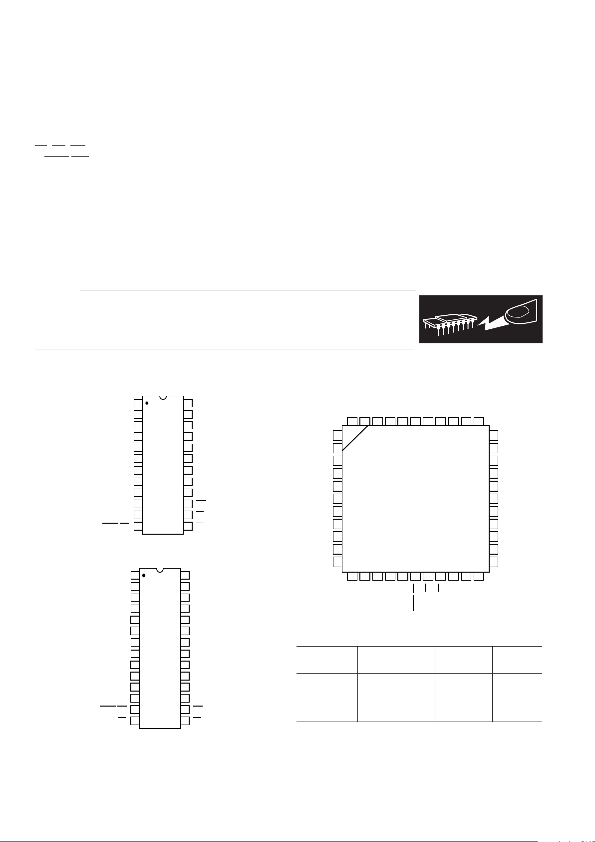
PIN CONFIGURATIONS
WARNING!
ESD SENSITIVE DEVICE
CAUTION
ESD (electrostatic discharge) sensitive device. Electrostatic charges as high as 4000 V readily
accumulate on the human body and test equipment and can discharge without detection. Although
the AD7776/AD7777/AD7778 feature proprietary ESD protection circuitry, permanent damage
may occur on devices subjected to high energy electrostatic discharges. Therefore, proper ESD
precautions are recommended to avoid performance degradation or loss of functionality.
24-Pin SOIC
1
2
24
23
22
10
15
11
12
14
13
21
20
18
17
16
19
9
3
4
5
TOP VIEW
(Not to Scale)
7
8
6
AD7776
DB2
DB3
DGND
DB4
DB5
DB6
DB7
DB1
DB0
C
REFIN
AGND
RTN
REFIN
A
IN
AGND
REFOUT
V
CC
DB8
(MSB) DB9
CLKIN
BUSY/INT
RD
WR
CS
28-Pin DIP & SOIC
1
2
24
23
22
10
15
11
12
14
13
21
20
17
16
9
3
4
5
7
8
6
18
19
TOP VIEW
(Not to Scale)
28
27
26
25
AD7777
NC
NC = NO CONNECT
DB2
DB3
DGND
DB4
DB5
DB6
DB7
DB1
DB0
DB8
(MSB) DB9
BUSY/INT
C
REFIN
AGND
RTN
REFIN
AGND
REFOUT
V
CC
CLKIN
RD
WR
CS
AIN4
A
IN
3
AIN2
A
IN
1
ORDERING GUIDE
Temperature No. of Package
Model Range Channels Option
1
AD7776AR2–40°C to +85°C 1 R-24
AD7777AN –40°C to +85°C 4 N-28
AD7777AR
2
–40°C to +85°C 4 R-28
AD7778AS
2
–40°C to +85°C 8 S-44
NOTES
1
R = SOIC, N = Plastic DIP, S = PQFP.
2
Analog Devices reserves the right to ship devices branded with a J in place of
the A, e.g., AD7776JR instead of AD7776AR. Temperature range remains
–40°C to +85°C.
44-Pin PQFP
7
8
9
10
11
6
5
4
3
2
1 33
32
31
30
29
28
27
26
25
24
23
18 19 20 21 221716151413
12
39 38 37 36 35 3444 43 42 41 40
TOP VIEW
(Not to Scale)
AD7778
NC
NC
NC
NC
NC
NC
NC
NC
NC
NC
NC
NC
NC
DB2
DB3
DGND
DB4
DB5
DB6
DB7
DB1
DB0
C
REFIN
RTN
AGND
REFIN
AIN8
AIN7
AIN6
AIN5
AIN4
AIN3
AIN2
AIN1
AGND
REFOUT
V
CC
DB8
(MSB) DB9
CLKIN
BUSY/INT
RD
WR
CS
NC = NO CONNECT
 Loading...