24-Bit, 312 kSPS, 109 dB Σ-Δ ADC
V
A–V
V
VIN–
www.BDTIC.com/ADI
with On-Chip Buffers and Serial Interface
FEATURES
High performance 24-bit ∑-∆ ADC
115 dB dynamic range at 78 kHz output data rate
109 dB dynamic range at 312 kHz output data rate
312 kHz maximum fully filtered output word rate
Pin-selectable oversampling rate (64×, 128×, and 256×)
Low power mode
Flexible SPI
Fully differential modulator input
On-chip differential amplifier for signal buffering
On-chip reference buffer
Full band low-pass finite impulse response (FIR) filter
Overrange alert pin
Digital gain correction registers
Power-down mode
Synchronization of multiple devices via
Daisy chaining
APPLICATIONS
Data acquisition systems
Vibration analysis
Instrumentation
GENERAL DESCRIPTION
The AD7764 is a high performance, 24-bit Σ- analog-to-digital
converter (ADC). It combines wide input bandwidth, high
speed, and performance of 109 dB dynamic range at a 312 kHz
output data rate. With excellent dc specifications, the converter
is ideal for high speed data acquisition of ac signals where dc
data is also required.
Using the AD7764 eases the front-end antialias filtering
equirements, simplifying the design process significantly. The
r
AD7764 offers pin-selectable decimation rates of 64×, 128×,
and 256×. Other features include an integrated buffer to drive
the reference as well as a fully differential amplifier to buffer
and level shift the input to the modulator.
An overrange alert pin indicates when an input signal has
exce
eded the acceptable range. The addition of internal gain
and internal overrange registers make the AD7764 a compact,
highly integrated data acquisition device requiring minimal
peripheral components.
The AD7764 also offers a low power mode, significantly
educing power dissipation without reducing the output data
r
rate or available input bandwidth.
SYNC
pin
AD7764
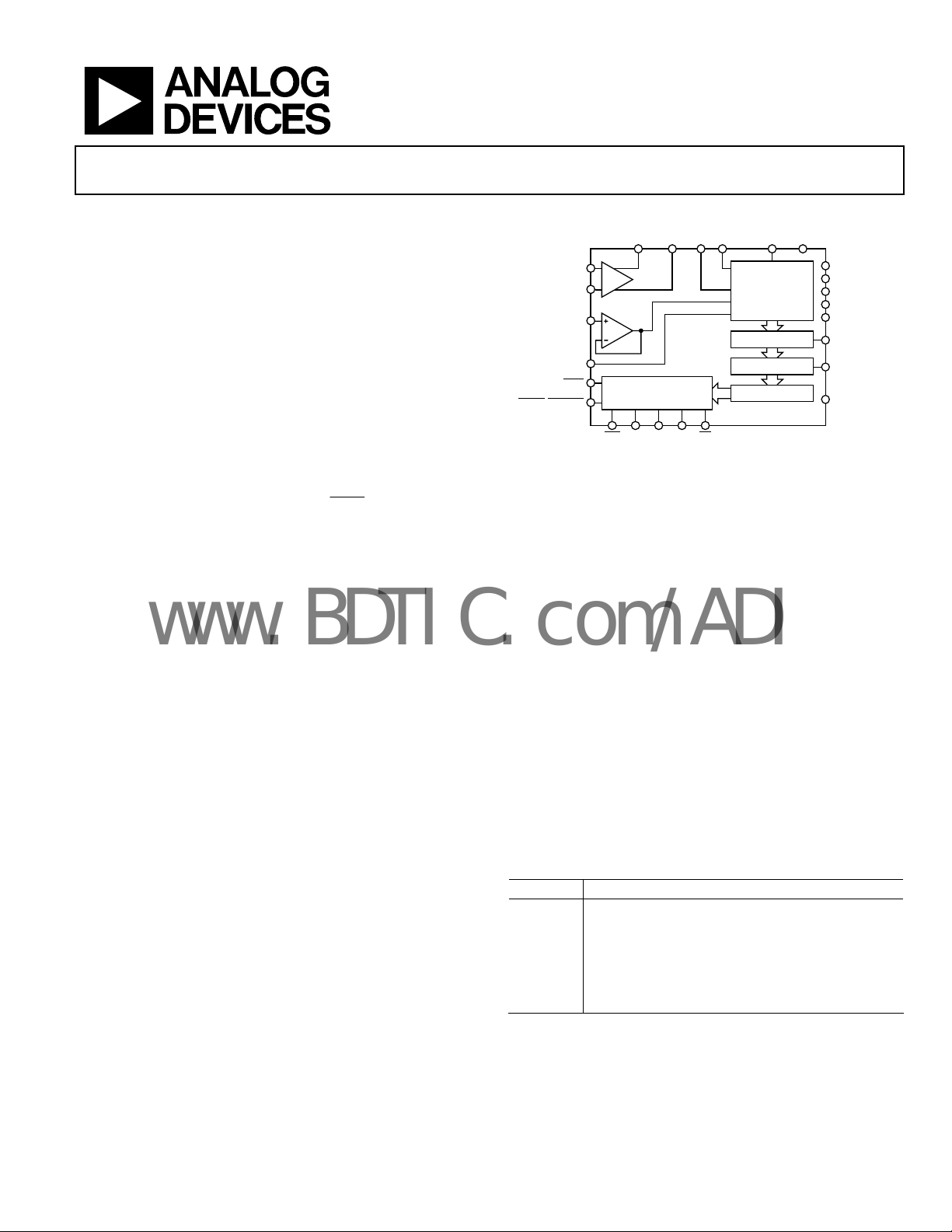
FUNCTIONAL BLOCK DIAGRAM
OUT
VINA+
DIFF
V
A–
IN
V
+
REF
BUF
REFGND
SYNC
RESET/PWRDWN
The differential input is sampled at up to 40 MSPS by an analog
modulator. The modulator output is processed by a series of
low-pass filters. The external clock frequency applied to the
AD7764 determines the sample rate, filter corner frequencies,
and output word rate.
The AD7764 device boasts a full band on-board FIR filter. The
ull stop-band attenuation of the filter is achieved at the Nyquist
f
frequency. This feature offers increased protection from signals
that lie above the Nyquist frequency being aliased back into the
input signal bandwidth.
The reference voltage supplied to the AD7764 determines the
i
nput range. With a 4 V reference, the analog input range is
±3.2768 V differential biased around a common mode of
2.048 V. This common-mode biasing can be achieved using
the on-chip differential amplifier, further reducing the external
signal conditioning requirements.
The AD7764 is available in a 28-lead TSSOP package and is
s
pecified over the industrial temperature range from −40°C
to +85°C.
Tabl e 1. Re l ate d D ev ice s
Part No. Description
AD7760 2.5 MSPS, 100 dB, parallel output on-chip buffers
AD7762 625 kSPS, 109 dB, parallel output on-chip buffers
AD7763 625 kSPS, 109 dB, serial output, on-chip buffers
AD7765 156 kSPS, 112 dB, serial output, on-chip buffers
AD7766 125 kSPS, 108 dB, serial output, 20 mW max power
AD7767 125 kSPS, 108 dB, serial output, 20 mW max Power
INTERFACE LOG IC AND
OFFSET AND GAIN
CORRECTION REGISTERS
FSO SCO SDI SDO FSI
OUT
A+
IN
Figure 1.
+
RECONSTRUCTION
FIR FILTER ENGINE
MULTIBIT
Σ-Δ
MODULATOR
DECIMATION
AD7764
GNDMCLK
AVDD1
AVDD2
AVDD3
AVDD4
DV
DD
OVERRANGE
DEC_RATE
R
BIAS
06518-001
Rev. 0
Information furnished by Analog Devices is believed to be accurate and reliable. However, no
responsibility is assumed by Anal og Devices for its use, nor for any infringements of patents or ot her
rights of third parties that may result from its use. Specifications subject to change without notice. No
license is granted by implication or otherwise under any patent or patent rights of Analog Devices.
Trademarks and registered trademarks are the property of their respective owners.
One Technology Way, P.O. Box 9106, Norwood, MA 02062-9106, U.S.A.
Tel: 781.329.4700 www.analog.com
Fax: 781.461.3113 ©2007 Analog Devices, Inc. All rights reserved.

AD7764
www.BDTIC.com/ADI
TABLE OF CONTENTS
Features.............................................................................................. 1
Applications....................................................................................... 1
General Description......................................................................... 1
Functional Block Diagram ..............................................................1
Revision History ...............................................................................2
Specifications..................................................................................... 3
Timing Specifications ..................................................................6
Timing Diagrams.......................................................................... 7
Absolute Maximum Ratings............................................................ 8
ESD Caution.................................................................................. 8
Pin Configuration and Function Descriptions............................. 9
Typical Performance Characteristics ........................................... 11
Terminology .................................................................................... 15
Theory of Operation ......................................................................16
Σ- Modulation and Digital Filtering...................................... 16
AD7764 Input Structure................................................................ 17
On-Chip Differential Amplifier ...............................................18
Modulator Input Structure........................................................ 19
AD7764 Interface............................................................................ 20
Reading Data............................................................................... 20
Reading Status and Other Registers......................................... 20
Writing to the AD7764 ..............................................................20
AD7764 Functionality.................................................................... 21
Synchronization.......................................................................... 21
Overrange Alerts ........................................................................21
Power Modes............................................................................... 21
Decimation Rate Pin.................................................................. 22
Daisy Chaining ............................................................................... 23
Reading Data in Daisy-Chain Mode ....................................... 23
Writing Data in Daisy-Chain Mode ........................................ 24
Clocking the AD7764 .................................................................... 25
MCLK Jitter Requirements ....................................................... 25
Decoupling and Layout Information........................................... 26
Supply Decoupling..................................................................... 26
Reference Voltage Filtering....................................................... 26
Differential Amplifier Components ........................................26
Layout Considerations............................................................... 26
Using the AD7764...................................................................... 27
Bias Resistor Selection............................................................... 27
AD7764 Registers........................................................................... 28
Control Register ......................................................................... 28
Status Register............................................................................. 28
Gain Register—Address 0x0004............................................... 29
Overrange Register—Address 0x0005..................................... 29
Outline Dimensions....................................................................... 30
Ordering Guide .......................................................................... 30
REVISION HISTORY
6/07—Revision 0: Initial Version
Rev. 0 | Page 2 of 32
AD7764
www.BDTIC.com/ADI
SPECIFICATIONS
AVDD1 = DVDD = V
using the on-chip amplifier with components, as shown in Tabl e 11 , unless otherwise noted.
Table 2.
Parameter Test Conditions/Comments Specification Unit
DYNAMIC PERFORMANCE
Decimate 256×
Normal Power Mode MCLK = 40 MHz, ODR = 78.125 kHz, f
Dynamic Range
110 dB min
Differential amplifier inputs shorted 113.4 dB typ
Signal-to-Noise Ratio (SNR)
106 dB min
Spurious-Free Dynamic Range (SFDR) Nonharmonic 130 dBFS typ
Total Harmonic Distortion (THD)
Input amplitude = −6 dB −103 dB typ
Input amplitude = −60 dB −71 dB typ
Low Power Mode MCLK = 40 MHz, ODR = 78.125 kHz, fIN = 1 kHz sine wave
Dynamic Range Modulator inputs shorted 113 dB typ
110 dB min
Differential amplifier inputs shorted 112 dB typ
Signal-to-Noise Ratio (SNR)
106 dB min
Total Harmonic Distortion (THD) Input amplitude = −0.5 dB −105 dB typ
Input amplitude = −6 dB −111 dB typ
Input amplitude = −6 dB −100 dB max
Input amplitude = −60 dB −76 dB typ
Decimate 128×
Normal Power Mode MCLK = 40 MHz, ODR = 156.25 kHz, fIN = 1 kHz sine wave
Dynamic Range
108 dB min
Differential amplifier inputs shorted 110.4 dB typ
Spurious-Free Dynamic Range (SFDR) Nonharmonic 130 dBFS typ
Intermodulation Distortion (IMD)
Low Power Mode MCLK = 40 MHz, ODR = 156.25 kHz, fiN = 1 kHz sine wave
Dynamic Range
Total Harmonic Distortion (THD) Input amplitude = −0.5 dB −105 dB typ
Input amplitude = −6 dB −111 dB typ
Input amplitude = −6 dB −100 dB max
Intermodulation Distortion (IMD) Input amplitude = −6 dB, fIN A = 50.3 kHz, fIN B = 47.3 kHz
Second-order terms −134 dB typ
Third-order terms −110 dB typ
= 2.5 V, AVDD2 = AVDD3 = AVDD4 = 5 V, V
DRIVE
2
2
2
Modulator inputs shorted 115 dB typ
Input amplitude = −0.5 dB 109 dB typ
Input amplitude = −0.5 dB −105 dB typ
Input amplitude = −0.5 dB 109 dB typ
Modulator inputs shorted 112 dB typ
Input amplitude = −0.5 dB −105 dB typ Total Harmonic Distortion (THD)
Input amplitude = −6 dB −103 dB typ
Input amplitude = −6 dB, fIN A = 50.3 kHz, fIN B = 47.3 kHz
Second-order terms −117 dB typ
Third-order terms −108 dB typ
Differential amplifier inputs shorted 109 dB typ
Input amplitude = −0.5 dB
+ = 4.096 V, MCLK amplitude = 5 V, TA = 25°C, normal power mode,
REF
= 1 kHz sine wave
IN
1
107 dB typ Signal-to-Noise Ratio (SNR)2
105 dB min
110 dB typ Modulator inputs shorted
109 dB min
107 dB typ Signal-to-Noise Ratio (SNR)
105 dB min
Rev. 0 | Page 3 of 32

AD7764
www.BDTIC.com/ADI
Parameter Test Conditions/Comments Specification Unit
Decimate 64×
Normal Power Mode MCLK = 40 MHz, ODR = 312.5 kHz, fIN = 1 kHz sine wave
Dynamic Range
Spurious-Free Dynamic Range (SFDR) Nonharmonic 130 dBFS typ
Intermodulation Distortion (IMD)
Low Power Mode
Dynamic Range
Signal-to-Noise Ratio (SNR)
102 dB min
Spurious-Free Dynamic Range (SFDR) Nonharmonic 110 dBFS typ
Total Harmonic Distortion (THD)
DC ACCURACY
Resolution Guaranteed monotonic to 24 bits 24 Bits
Integral Nonlinearity
Zero Error
Gain Error
Zero Error Drift
2
Modulator inputs shorted 109 dB typ
105 dB min
Differential amplifier inputs shorted 107.3 dB typ
104 dB typ Signal-to-Noise Ratio (SNR)2
102.7 dB min
Input amplitude = −0.5 dB −105 dB typ Total Harmonic Distortion (THD)
Input amplitude = −6 dB −103 dB typ
Input amplitude = −6 dB, fIN A = 100.3 kHz, fIN B = 97.3 kHz
Second-order terms −118 dB
Third-order terms −108 dB
106 dB typ Modulator inputs shorted
105 dB min
Differential amplifier inputs shorted 105.3
Input amplitude = −0.5 dB 103 dB typ
Input amplitude = −0.5 dB −105 dB typ
Input amplitude = −6 dB
Normal power mode 0.0036 % typ
Low power mode 0.0014 % typ
Normal power mode 0.006 % typ
0.03 % max
Including on-chip amplifier 0.04 % typ
Low power mode 0.002 % typ
0.024 % max
0.018 % typ
Including on-chip amplifier 0.04 % typ
0.00006 %FS/°C t
−111 dB typ
−100 dB max
yp
Gain Error Drift
DIGITAL FILTER CHARACTERISTICS
Pass-Band Ripple 0.1 dB typ
Pass Band
−3 dB Bandwidth
Stop Band
Group Delay
ANALOG INPUT
Differential Input Voltage
Input Capacitance At on-chip differential amplifier inputs 5 pF typ
At modulator inputs 29 pF typ
3
3
3
Decimate 64× MCLK = 40 MHz 89 µs typ
Decimate 128× MCLK = 40 MHz 177 µs typ
Decimate 256× MCLK = 40 MHz 358 µs typ
0.00005 %FS/°C t
−1 dB frequency ODR × 0.4016 kHz
ODR × 0.4096 kHz
Beginning of stop band ODR × 0.5 kHz
Decimate 64× and decimate 128× modes −120 dB typ Stop-Band Attenuation
Decimate 256× −115 dB typ
Modulator input pins: VIN(+) − VIN(−), V
Rev. 0 | Page 4 of 32
+ = 4.096 V ±3.2768 V p-p
REF
yp

AD7764
www.BDTIC.com/ADI
Parameter Test Conditions/Comments Specification Unit
REFERENCE INPUT/OUTPUT
V
Input Voltage AVDD3 = 5 V ± 5% 4.096 V
REF
V
Input DC Leakage Current ±1 µA max
REF
V
Input Capacitance 5 pF typ
REF
DIGITAL INPUT/OUTPUT
MCLK Input Amplitude 2.25 to 5.25 V
Input Capacitance 7.3 pF typ
Input Leakage Current ±1 A/pin max
V
0.8 × DVDD V min
INH
V
0.2 × DVDD V max
INL
4
V
OH
VOL 0.1 V max
ON-CHIP DIFFERENTIAL AMPLIFIER
Input Impedance >1 MΩ
Bandwidth for 0.1 dB Flatness 125 kHz
Common-Mode Input Voltage Voltage range at input pins: VINA+ and VINA− −0.5 to +2.2 V
Common-Mode Output Voltage On-chip differential amplifier pins: V
POWER REQUIREMENTS
AVDD1 (Modulator Supply) ±5% 2.5 V
AVDD2 (General Supply) ±5% 5 V
AVDD3 (Differential Amplifier Supply) ±5% 5 V min/max
AVDD4 (Ref Buffer Supply) ±5% 5 V min/max
DVDD ±5% 2.5 V
Normal Power Mode
AIDD1 (Modulator) 19 mA typ
AIDD2 (General)
5
AIDD3 (Differential Amplifier) AVDD3 = 5 V 10 mA typ
AIDD4 (Reference Buffer) AVDD4 = 5 V 9 mA typ
5
DI
DD
Low Power Mode
AIDD1 (Modulator) 10 mA typ
AIDD2 (General)
5
AIDD3 (Differential Amplifier) AVDD3 = 5 V 5.5 mA typ
AIDD4 (Reference Buffer) AVDD4 = 5 V 5 mA typ
5
DI
DD
POWER DISSIPATION
Normal Power Mode 300 mW typ
Low Power Mode MCLK = 40 MHz, decimate 64× 160 mW typ
215 mW max
Power-Down Mode6
1
See Terminology section.
2
SNR specifications in decibels are referred to a full-scale input, FS. Tested with an input signal at 0.5 dB below full scale, unless otherwise specified.
3
Output Data Rate (ODR) = [(MCLK/2)]/Decimation Rate. That is, the maximum ODR for AD7764 = [(40 MHz)/2)/64] = 312.5 kHz.
4
Tested with a 400 µA load current.
5
Tested at MCLK = 40 MHz. This current scales linearly with MCLK frequency applied.
6
Tested at 125°C.
2.2 V min
OUT
+ and V
− 2.048 V
OUT
MCLK = 40 MHz 13 mA typ
MCLK = 40 MHz 37 mA typ
MCLK = 40 MHz 7 mA typ
MCLK = 40 MHz 20 mA typ
MCLK = 40 MHz, decimate 64×
371 mW max
PWRDWN
held logic low
1 mW t
yp
Rev. 0 | Page 5 of 32
AD7764
www.BDTIC.com/ADI
TIMING SPECIFICATIONS
AVDD1 = DVDD = 2.5 V, AVDD2 = AVDD3 = AVDD4 = 5 V, V
Tabl e 3.
Parameter Limit at T
f
500 kHz min Applied master clock frequency
MCLK
, T
Unit Description
MIN
MAX
40 MHz max
f
250 kHz min Internal modulator clock derived from MCLK
ICLK
20 MHz max
t1 1 × t
t2 1 × t
typ SCO high period
ICLK
typ SCO low period
ICLK
t3 1 ns typ SCO rising edge to FSO falling edge
t4 2 ns typ
t5 8 ns max MSB data access time, SDO active to SDO valid
t6 40 ns min Data hold time (SDO valid to SCO rising edge)
t7 9.5 ns max Data access time (SCO rising edge to SDO valid)
t8 2 ns typ
t9 32 × t
max
SCO
t10 12 ns min
t11 1 × t
1
t
32 × t
12
min
SCO
max
SCO
t13 12 ns min SDI setup time for the first data bit
t14 12 ns min SDI setup time
t15 0 ns max SDI hold time
1
This is the maximum time
FSI
can be held low when writing to an individual device (a device that is not daisy-chained).
+ = 4.096 V, TA = 25°C, C
REF
Data access time, FSO
SCO rising edge to FSO
low period
FSO
Setup time from FSI
low period
FSI
low period
FSI
= 25 pF.
LOAD
falling edge to data active
rising edge
falling edge to SCO falling edge
Rev. 0 | Page 6 of 32
AD7764
www.BDTIC.com/ADI
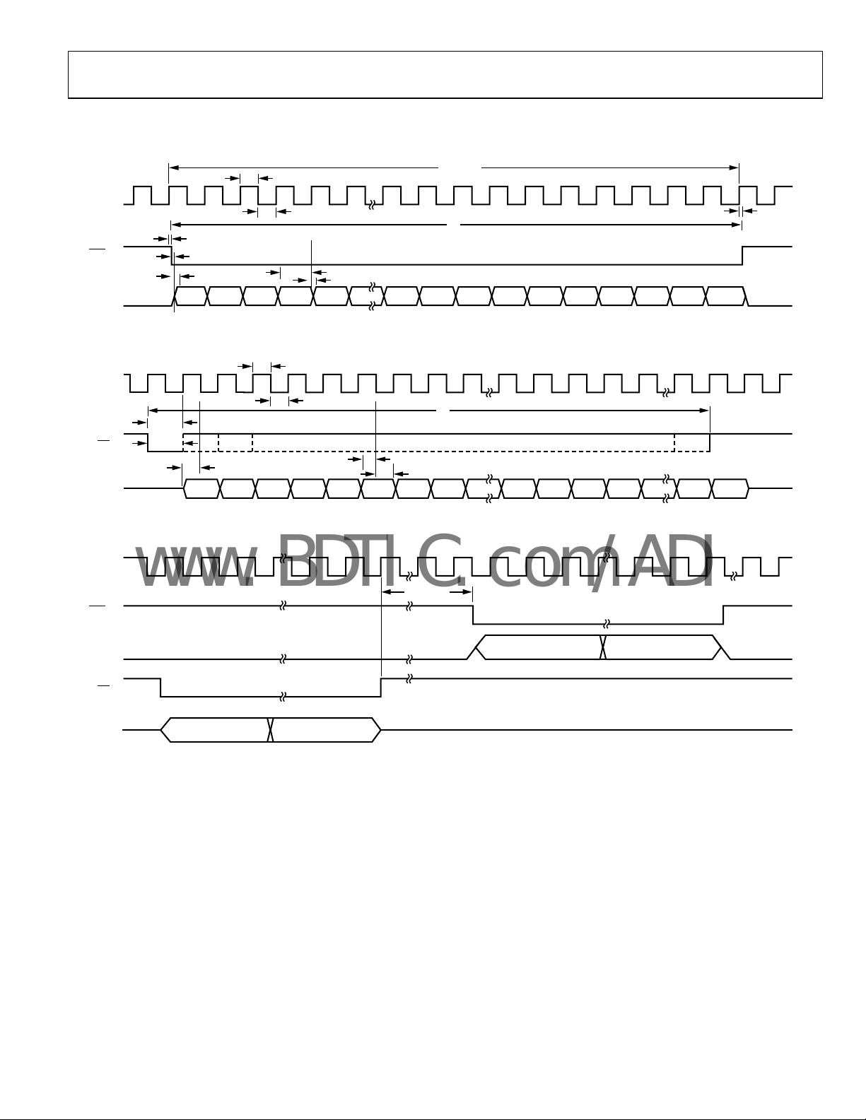
TIMING DIAGRAMS
32 ×
t
SCO
t
t
9
t
12
8
6518-002
06518-003
SCO (O)
FSO (O)
SDO (O)
SCO (O)
FSI (I)
SDI (I)
t
1
t
2
t
3
t
4
t
5
D22D23 D21 D20 D19 D1 D0 ST4 ST 3 ST2 ST 1 ST0 0 0 0
t
6
t
7
Figure 2. Serial Read Timing Diagram
t
1
t
2
t
10
t
11
t
13
RA15 RA14 RA13 RA12 RA11 RA10 RA9 RA8 RA1 RA0 D15 D14 D1 D0
t
14
t
15
Figure 3. AD7764 Register Write
SCO (O)
FSO (O)
SDO (O)
FSI (I)
SDI (I)
CONTROL REG ISTER
ADDR (0x0001)
CONTROL REGISTER
INSTRUCTION
Figure 4. AD7764 Status Register Read Cycle
≥8 ×
t
SCO
STATUS REGISTER
CONTENTS [31:16]
NEXT DATA READ FO LLOW ING THE W RITE TO CONTROL REGISTER
DON’T CARE
BITS [15:0]
06518-004
Rev. 0 | Page 7 of 32
AD7764
www.BDTIC.com/ADI
ABSOLUTE MAXIMUM RATINGS
TA = 25°C, unless otherwise noted.
Table 4.
Parameter Rating
AV
1 to GND −0.3 V to +2.8 V
DD
AVDD2, AVDD3, AVDD4 to GND −0.3 V to +6 V
DV
to GND −0.3 V to +2.8 V
DD
VINA+ , VINA− to GND
VIN+ , VIN− to GND
1
−0.3 V to +6 V
1
−0.3 V to +6 V
Digital Input Voltage to GND2 −0.3 V to +2.8 V
V
+ to GND
REF
3
−0.3 V to +6 V
AGND to DGND −0.3 V to +0.3 V
Input Current to Any Pin Except Supplies
Operating Temperature Range
4
±10 mA
Commercial −40°C to +85°C
Storage Temperature Range −65°C to +150°C
Junction Temperature 150°C
TSSOP Package
θ
Thermal Impedance 143°C/W
JA
θ
Thermal Impedance 45°C/W
JC
Lead Temperature, Soldering
Vapor Phase (60 sec) 215°C
Infrared (15 sec) 220°C
ESD 1 kV
1
Absolute maximum voltage for VIN−, VIN+, VINA−, and VINA+ is 6.0 V or
AVDD3 + 0.3 V, whichever is lower.
2
Absolute maximum voltage on digital inputs is 3.0 V or DV
whichever is lower.
3
Absolute maximum voltage on V
whichever is lower.
4
Transient currents of up to 100 mA do not cause SCR latch-up.
+ input is 6.0 V or AVDD4 + 0.3 V,
REF
+ 0.3 V,
DD
Stresses above those listed under Absolute Maximum Ratings
y cause permanent damage to the device. This is a stress
ma
rating only; functional operation of the device at these or any
other conditions above those listed in the operational sections
of this specification is not implied. Exposure to absolute
maximum rating conditions for extended periods may affect
device reliability.
ESD CAUTION
Rev. 0 | Page 8 of 32
AD7764
www.BDTIC.com/ADI
PIN CONFIGURATION AND FUNCTION DESCRIPTIONS
V
IN
V
OUT
V
IN
V
OUT
V
V
AV
DD
AGND3
OVERRANGE
SCO
FSO
SDO
SDI
FSI
A–
A+
A+
A–
–
IN
+
IN
2
1
2
3
4
5
6
AD7764
TOP VIEW
7
(Not to Scale)
8
9
10
11
12
13
14
28
3
AV
DD
27
V
+
REF
26
REFGND
25
AV
4
DD
24
1
AV
DD
23
AGND1
22
R
BIAS
21
AV
2
DD
20
AGND2
19
MCLK
18
DEC_RATE
17
DV
DD
16
RESET/PWRDWN
15
SYNC
06518-005
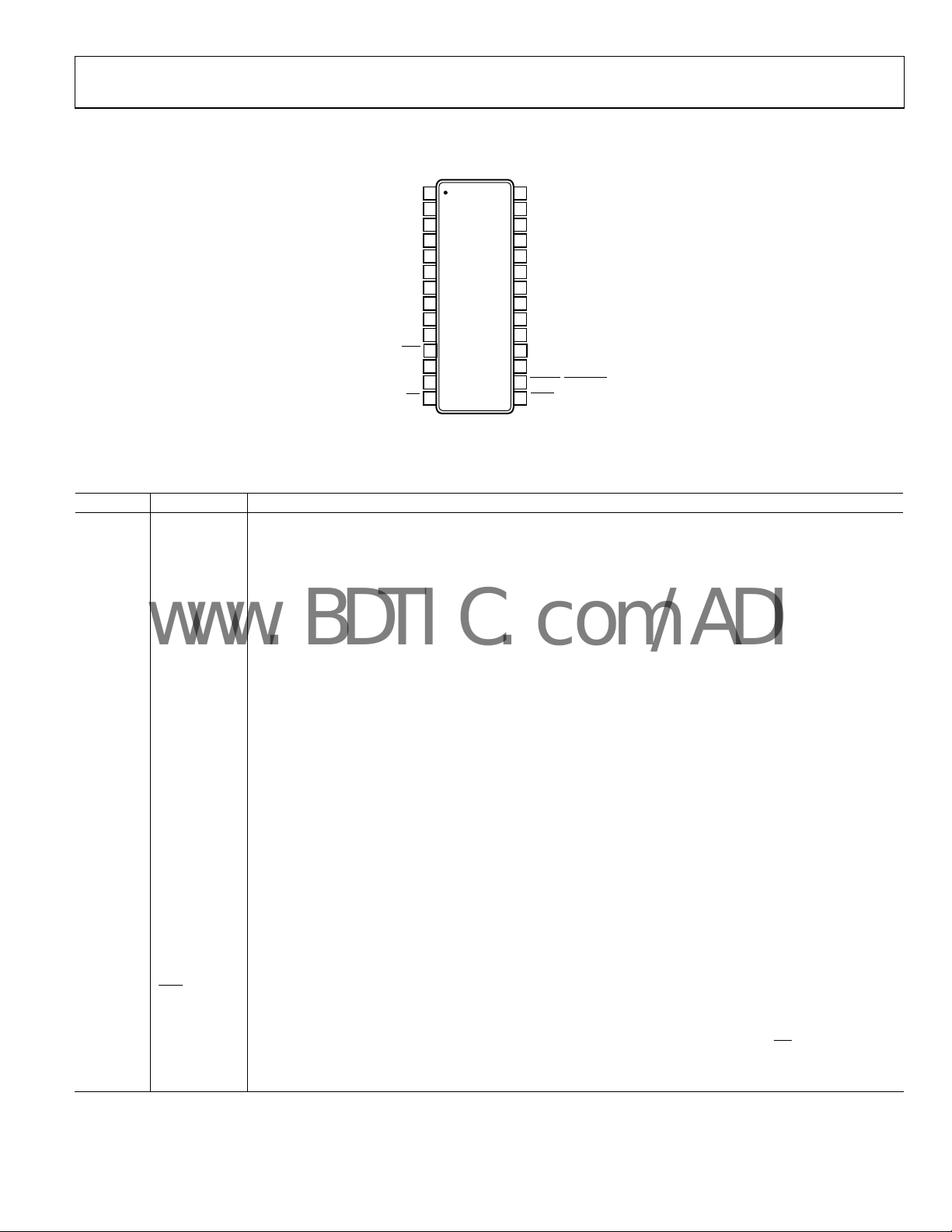
Figure 5. 28-Lead TSSOP Pin Configuration
Table 5. Pin Function Descriptions
Pin No. Mnemonic Description
24 AVDD1 2.5 V Power Supply for Modulator. This pin should be decoupled to AGND1 (Pin 23) with a 100 nF capacitor.
7 and 21 AVDD2
5 V Power Supply. Pin 7 should be decoupled to AGND3 (P
in 8) with a 100 nF capacitor. Pin 21 should be
decoupled to AGND1 (Pin 23) with a 100 nF capacitor.
28 AVDD3
3.3 V to 5 V Power Supply for Differential Amplifier. This pin shou
ld be decoupled to the ground plane with
a 100 nF capacitor.
25 AVDD4
3.3 V to 5 V Power Supply for Reference Buffer. This pin should be dec
oupled to AGND1 (Pin 23) with a 100 nF
capacitor.
17 DVDD
2.5 V Power Supply for Digital Circuitry and FIR Filter. This pin sh
ould be decoupled to the ground plane with
a 100 nF capacitor.
22 R
BIAS
Bias Current Setting Pin. A resistor must be inserted bet
ween this pin and AGND. For more details, see the
Bias Resistor Selection section.
23 AGND1 Power Supply Ground for Analog Circuitry.
20 AGND2 Power Supply Ground for Analog Circuitry.
8 AGND3 Power Supply Ground for Analog Circuitry.
26 REFGND Reference Ground. Ground connection for the reference voltage.
27 V
+ Reference Input.
REF
1 VINA− Negative Input to Differential Amplifier.
2 V
A+ Positive Output from Differential Amplifier.
OUT
3 VINA+ Positive Input to Differential Amplifier.
4 V
A− Negative Output from Differential Amplifier.
OUT
5 VIN− Negative Input to the Modulator.
6 VIN+ Positive Input to the Modulator.
9 OVERRANGE
Overrange Pin. This pin outputs a logic high to indicate tha
t the user has applied an analog input that is
approaching the limit of the analog input to the modulator.
10 SCO
Serial Clock Out. This clock signal is derived from the int
ernal ICLK signal. The frequency of this clock is equal
to ICLK. See the Clocking the AD7764 section for further details.
11
FSO
12 SDO
Frame Sync Out. This signal frames the ser
Serial Data Out. Data and status are output on this pin during each ser
ial data output and is 32 SCO periods wide.
ial transfer. Each bit is clocked out on an
SCO rising edge and is valid on the falling edge. See the AD7764 Interface section for further details.
13 SDI
Serial Data In. The first data bit (MSB) must be v
alid on the next SCO falling edge after the FSI
event is latched.
32 bits are required for each write; the first 16-bit word contains the device and register address, and the
second word contains the data. See the AD7764 Interface section for further details.
Rev. 0 | Page 9 of 32

AD7764
www.BDTIC.com/ADI
Pin No. Mnemonic Description
14
15
16
19 MCLK
18 DEC_RATE
FSI
SYNC
RESET
/
PWRDWN
Frame Sync Input. The status of this pin is checked on the falling edge of SCO. If this pin is low, then the first
data bit is latched in on the next SCO falling edge. See the AD7764 Interface section for further details.
Synchronization Input. A falling edge on this pin resets the internal filter. This can be used to synchronize
multiple devices in a system. See the Synchronization section for further details.
Reset/Power-down Pin. When a logic low is sensed on this pin, the part is powered down and all internal
circuitry is reset.
Master Clock Input. A low jitter digital clock must be applied t
frequency of this clock. See the Clocking the AD7764 section for more details.
Decimation Rate. This pin selects one of the three decimation rate modes. When 2.5 V is applied to this pin,
a decima
decimation rate of 256× is selected by setting the pin to ground.
tion rate 64× is selected. A decimation rate of 128× is selected by leaving the pin floating. A
o this pin. The output data rate depends on the
Rev. 0 | Page 10 of 32
 Loading...