625 kSPS, 24-Bit, 109 dB Σ−Δ ADC
FEATURES
120 dB dynamic range at 78 kHz output data rate
109 dB dynamic range at 625 kHz output data rate
112 dB SNR at 78 kHz output data rate
106 dB SNR at 625 kHz output data rate
625 kHz maximum fully filtered output word rate
Programmable over-sampling rate (32× to 256×)
Fully differential modulator input
On-chip differential amplifier for signal buffering
Low-pass finite impulse response (FIR) filter with default or
user-programmable coefficients
Overrange alert bit
Digital offset and gain correction registers
Filter bypass modes
Low power and power-down modes
Synchronization of multiple devices via
APPLICATIONS
Data acquisition systems
Vibration analysis
Instrumentation
GENERAL DESCRIPTION
SYNC
pin
V
REF+
MCLK
SYNC
RESET
With On-Chip Buffer
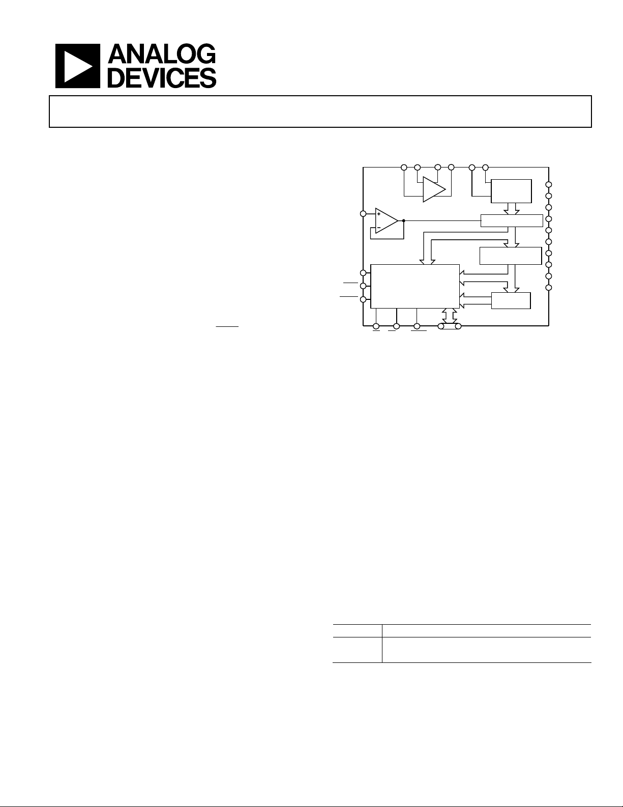
FUNCTIONAL BLOCK DIAGRAM
V
V
IN+
IN–
MULTIBIT
Σ-Δ
MODULATOR
RECONSTRUCTION
PROGRAMMABLE
DECIMATION
FIR FILTER
ENGINE
BUF
AD7762
CONTROL LOGIC
OFFSET AND GAIN
REGISTERS
DIFF
I/O
DB0 TO DB15CS DRDYRD/WR
Figure 1.
AD7762
AV
DD1
AV
DD2
AV
DD3
AV
DD4
DECAPA/B
R
BIAS
AGND
V
DRIVE
DV
DD
DGND
05477-001
The AD7762 is a high performance, 24-bit Σ- analog-todigital converter (ADC). It combines wide input bandwidth
and high speed with the benefits of Σ- conversion with a
performance of 106 dB SNR at 625 kSPS, making it ideal for
high speed data acquisition. Wide dynamic range combined
with significantly reduced antialiasing requirements simplify
the design process. An integrated buffer to drive the reference,
a differential amplifier for signal buffering and level shifting, an
overrange flag, internal gain and offset registers, and a low-pass
digital FIR filter make the AD7762 a compact, highly integrated
data acquisition device requiring minimal peripheral component selection. In addition, the device offers programmable
decimation rates, and the digital FIR filter can be adjusted if
the default characteristics are not appropriate to the application.
The AD7762 is ideal for applications demanding high SNR
without a complex front end signal processing design.
The differential input is sampled at up to 40 MSPS by an analog
modulator. The modulator output is processed by a series of lowpass filters, the final filter having default or user-programmable
Rev. 0
Information furnished by Analog Devices is believed to be accurate and reliable. However, no
responsibility is assumed by Anal og Devices for its use, nor for any infringements of patents or ot her
rights of third parties that may result from its use. Specifications subject to change without notice. No
license is granted by implication or otherwise under any patent or patent rights of Analog Devices.
Trademarks and registered trademarks are the property of their respective owners.
coefficients. The sample rate, filter corner frequencies, and output
word rate are set by a combination of the external clock frequency
and the configuration registers of the AD7762.
The reference voltage supplied to the AD7762 determines the
analog input range. With a 4 V reference, the analog input range
is ±3.2 V differential biased around a common mode of 2 V.
This common-mode biasing can be achieved using the on-chip
differential amplifier, further reducing the external signal
conditioning requirements.
The AD7762 is available in an exposed paddle, 64-lead TQFP
and is specified over the industrial temperature range from
−40°C to +85°C.
Table 1. Related Devices
Part No. Description
AD7760 24-bit, 2.5 MSPS, 100 dB Σ-∆, parallel interface
AD7763 24-bit, 625 kSPS, 109 dB Σ-∆, serial interface
One Technology Way, P.O. Box 9106, Norwood, MA 02062-9106, U.S.A.
Tel: 781.329.4700 www.analog.com
Fax: 781.461.3113 © 2005 Analog Devices, Inc. All rights reserved.

AD7762
TABLE OF CONTENTS
General Description......................................................................... 1
Bias Resistor Selection............................................................... 17
Specifications..................................................................................... 3
Timing Specifications....................................................................... 5
Timing Diagrams.......................................................................... 5
Absolute Maximum Ratings............................................................ 6
ESD Caution.................................................................................. 6
Pin Configuration and Function Descriptions............................. 7
Terminology ......................................................................................9
Typical Performance Characteristics........................................... 10
Theory of Operation ......................................................................13
AD7762 Interface............................................................................ 14
Reading Data............................................................................... 14
Sharing the Parallel Bus............................................................. 14
Writing to the AD7762.............................................................. 14
Reading Status and Other Registers......................................... 14
Clocking the AD7762 ................................................................ 15
Decoupling and Layout Recommendations................................ 18
Supply Decoupling..................................................................... 19
Additional Decoupling.............................................................. 19
Reference Voltage Filtering .......................................................19
Differential Amplifier Components ........................................19
Layout Considerations............................................................... 19
Programmable FIR Filter............................................................... 20
Downloading a User-Defined Filter ............................................ 21
Example Filter Download ......................................................... 21
AD7762 Registers........................................................................... 23
Control Register 1—Reg 0x0001.............................................. 23
Control Register 2—Address 0x0002 ...................................... 23
Status Register (Read Only)...................................................... 24
Offset Register—Address 0x0003............................................. 24
Gain Register—Address 0x0004............................................... 24
Example 1 ....................................................................................15
Example 2 ....................................................................................15
Driving the AD7762....................................................................... 16
Using the AD7762...................................................................... 17
REVISION HISTORY
8/05—Revision 0: Initial Version
Overrange Register—Address 0x0005..................................... 24
Outline Dimensions....................................................................... 25
Ordering Guide .......................................................................... 25
Rev. 0 | Page 2 of 28

AD7762
SPECIFICATIONS
AV
= DVDD = V
DD1
using on-chip amplifier with components as shown in
Table 2.
Parameter Test Conditions/Comments Specification Unit
DYNAMIC PERFORMANCE
Decimate by 256 MCLK = 40 MHz, ODR = 78 kHz, FIN = 1 kHz
Dynamic Range Modulator inputs shorted 119
Signal-to-Noise Ratio (SNR)
Input amplitude = −60 dBFS 59 dB typ
Spurious-Free Dynamic Range (SFDR) Nonharmonic, input amplitude = −6 dBFS 126 dBc typ
Input amplitude = −60 dBFS 77 dBc typ
Total Harmonic Distortion (THD) Input amplitude = −0.5 dBFS −105 dB typ
Input amplitude = −6 dBFS −106 dB typ
Input amplitude = −60 dBFS −75 dB typ
Decimate by 64 MCLK = 40 MHz, ODR = 312.5 kHz, FIN = 1 kHz
Dynamic Range Modulator inputs shorted 112
Signal-to-Noise Ratio (SNR)
Spurious-Free Dynamic Range (SFDR) Nonharmonic, input amplitude = −6 dBFS 126 dBc typ
Decimate by 32 MCLK = 40 MHz, ODR = 625 kHz, FIN =100 kHz
Dynamic Range Modulator inputs shorted 108
Signal-to-Noise Ratio (SNR)
Spurious-Free Dynamic Range (SFDR) Nonharmonic, input amplitude = −6 dBFS 120 dBc typ
Total Harmonic Distortion (THD) Input amplitude = −0.5 dBFS −108 dB typ
Input amplitude = −6 dBFS −106 dB typ
DC ACCURACY
Resolution 24 Bits
Differential Nonlinearity Guaranteed monotonic to 24 bits
Integral Nonlinearity 0.00076 % typ
Zero Error 0.014 % typ
0.02 % max
Gain Error 0.015 % typ
Zero Error Drift 0.019 %/°C typ
Gain Error Drift 0.0002 %/°C typ
DIGITAL FILTER RESPONSE
Decimate by 32
Group Delay MCLK = 40 MHz 47 µs typ
Decimate by 64
Group Delay MCLK = 40 MHz 91.5 µs typ
Decimate by 256
Group Delay MCLK = 40 MHz 358 µs typ
ANALOG INPUT
Differential Input Voltage VIN(+) – VIN(−), V
V
Input Capacitance At internal buffer inputs 5 pF typ
At modulator inputs 55 pF typ
= 2.5 V, AV
DRIVE
DD2
= AV
DD3
= AV
= 5 V, V
DD4
= 4.096 V, MCLK amplitude = 5 V, TA = 25°C, normal mode,
REF
Table 8, unless otherwise noted.
1
dB min
2
Input amplitude = −0.5 dBFS 112 dB typ
120.5
dB typ
dB min
2
Input amplitude = −0.5 dBFS 109.5 dB typ
114
dB typ
dB min
2
Input amplitude = −0.5 dBFS 107 dB typ
= 2.5 V ±2 V p-p
REF
(+) – VIN(−), V
IN
= 4.096 V ±3.25 V p-p
REF
Rev. 0 | Page 3 of 28
109.5
dB typ

AD7762
Parameter Test Conditions/Comments Specification Unit
REFERENCE INPUT/OUTPUT
V
Input Voltage V
REF
V
V
Input DC Leakage Current ±6 µA max
REF
V
Input Capacitance 5 pF max
REF
POWER DISSIPATION
Total Power Dissipation Normal mode 958 mW max
Low power mode 661 mW max
Standby Mode Clock stopped 6.35 mW max
POWER REQUIREMENTS
AV
(Modulator Supply) ±5% +2.5 V
DD1
AV
(General Supply) ±5% +5 V
DD2
AV
(Diff Amp Supply) +3.15/+5.25 V min/max
DD3
AV
(Ref Buffer Supply) +3.15/+5.25 V min/max
DD4
DVDD ±5% +2.5 V
V
+1.65/+2.7 V min/max
DRIVE
Normal Mode
AI
(Modulator) 49/51 mA typ/max
DD1
AI
(General) 40/42 mA typ/max
DD2
AI
(Reference Buffer) AV
DD4
Low Power Mode
AI
(Modulator) 26/28 mA typ/max
DD1
AI
(General) 20/23 mA typ/max
DD2
AI
(Reference Buffer) AV
DD4
AI
(Diff Amp) AV
DD3
DIDD Both modes 63/70 mA typ/max
DIGITAL I/O
MCLK Input Amplitude
3
Input Capacitance 7.3 pF typ
Input Leakage Current ±5 A max
Three-State Leakage Current (D15:D0) ±5 A max
V
0.7 × V
INH
V
0.3 × V
INL
4
V
OH
4
V
OL
1
See the Terminology section.
2
SNR specifications in dBs are referred to a full-scale input, FS. Tested with an input signal at 0.5 dB below full scale, unless otherwise specified.
3
While the AD7762 can function with an MCLK amplitude of less than 5 V, this is the recommended amplitude to achieve the performance as stated.
4
Tested with a 400 µA load current.
= 3.3 V ± 5% +2.5 V max
DD3
= 5 V ± 5% +4.096 V max
DD3
= 5 V 34/36 mA typ/max
DD4
= 5 V 9/10 mA typ/max
DD4
= 5 V, both modes 41/44 mA typ/max
DD3
5 V typ
V min
DRIVE
V max
DRIVE
1.5 V min
0.1 V max
Rev. 0 | Page 4 of 28
AD7762
TIMING SPECIFICATIONS
AV
= DVDD = V
DD1
Table 3.
Parameter Limit at T
f
1 MHz min Applied master clock frequency
MCLK
40 MHz max
f
500 kHz min Internal modulator clock derived from MCLK
ICLK
20 MHz max
1, 2
t
1
t2 10 ns min
t3 3 ns min
t4 (0.5 × t
t5 t
t6 t
t7 3 ns min
t8 11 ns max Bus relinquish time
t9 4 × t
t10 4 × t
t11 5 ns min Data setup time
t12 0 ns min Data hold time
1
t
= 1/f
ICLK
.
ICLK
2
When ICLK = MCLK,
DRIVE
0.5 × t
= 2.5 V, AV
MIN
typ
ICLK
= AV
DD2
, T
Unit Description
MAX
DD3
= AV
= 5 V, TA = 25°C, normal mode, unless otherwise noted.
DD4
DRDY pulse width
DRDY falling edge to CS falling edge
RD/WR setup time to CS falling edge
) + 16 ns max Data access time
ICLK
min
ICLK
min
ICLK
CS low read pulse width
CS high pulse width between reads
RD/WR hold time to CS rising edge
min
ICLK
min
ICLK
DRDY
pulse width depends on the mark/space ratio of applied MCLK.
CS low write pulse width
CS high period between address and data
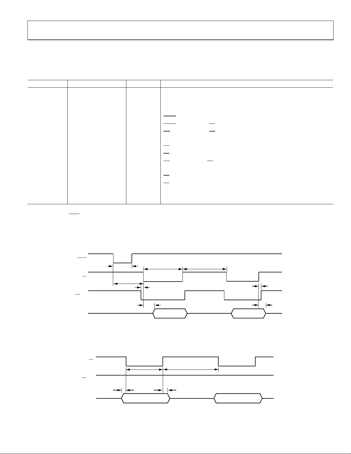
TIMING DIAGRAMS
DRDY
RD/WR
D[0:15]
CS
CS
RD/WR
D[0:15]
t
1
t
2
t
5
t
3
t
4
DATA MSW LSW + STATUS
Figure 2. Parallel Interface Timing Diagram
t
9
t
11
REGISTER ADDRESS REGISTER DATA
t
12
t
6
t
7
t
8
05477-002
t
10
05477-004
Figure 3. AD7762 Register Write
Rev. 0 | Page 5 of 28
AD7762
ABSOLUTE MAXIMUM RATINGS
TA = 25°C, unless otherwise noted.
Table 4.
Parameters Rating
AV
to GND −0.3 V to +3 V
DD1
AV
–AV
DD2
to GND −0.3 V to +6 V
DD4
DVDD to GND −0.3 V to +3 V
V
to GND −0.3 V to +3 V
DRIVE
V
, V
to GND −0.3 V to +6 V
IN+
IN–
Digital input voltage to GND1 −0.3 V to DV
+ 0.3 V
DD
−0.3 V to +6 V MCLK to MCLKGND
V
to GND2 −0.3 V to AV
REF
DD4
+ 0.3 V
AGND to DGND −0.3 V to +0.3 V
Input Current to Any Pin
Except Supplies
3
Operating Temperature Range
±10 mA
−40°C to +85°C Commercial
−65°C to +150°C Storage Temperature Range
150°C Junction Temperature
TQFP Exposed Paddle Package
θJA Thermal Impedance 92.7°C/W
θJC Thermal Impedance 5.1°C/W
Lead Temperature, Soldering
215°C Vapor Phase (60 sec)
220°C Infrared (15 sec)
ESD 600 V
1
Absolute maximum voltage on digital inputs is 3.0 V or DVDD + 0.3 V,
whichever is lower.
2
Absolute maximum voltage on V
whichever is lower.
3
Transient currents of up to 200 mA do not cause SCR latch-up.
input is 6.0 V or AV
REF
+ 0.3 V,
DD4
Stresses above those listed under Absolute Maximum Ratings
may cause permanent damage to the device. This is a stress
rating only; functional operation of the device at these or any
other conditions above those listed in the operational sections
of this specification is not implied. Exposure to absolute
maximum rating conditions for extended periods may affect
device reliability.
ESD CAUTION
ESD (electrostatic discharge) sensitive device. Electrostatic charges as high as 4000 V readily accumulate on the
human body and test equipment and can discharge without detection. Although this product features
proprietary ESD protection circuitry, permanent damage may occur on devices subjected to high energy
electrostatic discharges. Therefore, proper ESD precautions are recommended to avoid performance
degradation or loss of functionality.
Rev. 0 | Page 6 of 28
AD7762
E
PIN CONFIGURATION AND FUNCTION DESCRIPTIONS
DRIV
DGND63V
DGND61DB060DB159DB258DB357DB456DB555DB654DB753DGND52DB851DB950DB1049DB11
64
62
31
AGND332AGND3
DECAPB
48
47
46
45
44
43
42
41
40
39
38
37
36
35
34
33
DB12
DB13
DB14
DB15
V
DRIVE
DGND
DGND
DV
DD
CS
RD/WR
DRDY
RESET
SYNC
DGND
AGND1
AV
DD1
05477-005
DGND
MCLKGND
MCLK
AV
DD2
AGND2
AV
DD1
AGND1
DECAPA
REFGND
V
REF+
AGND4
AV
DD4
AGND2
AV
DD2
AV
DD2
AGND2
1
PIN 1
2
3
4
5
6
7
8
9
10
11
12
13
14
15
16
17
18
19
20
A+
BIAS
IN
R
V
AGND2
21
A–
IN
V
AD7762
TOP VIEW
(Not to Scale)
22
23
A–
A+
OUT
OUT
V
V
24
DD3
AV
AGND3
25
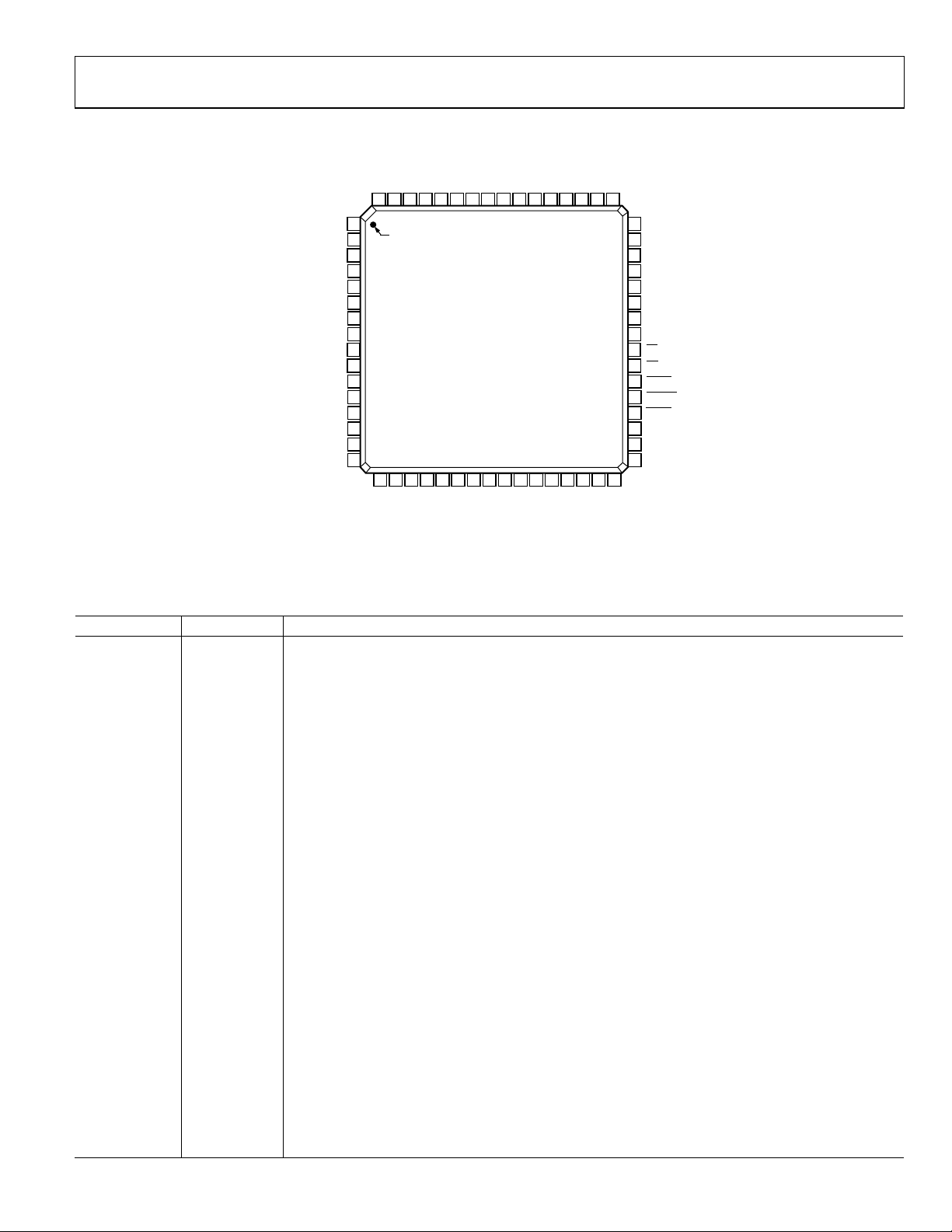
Figure 4. 64-Lead TQFP Pin Configuration
26
27
28
DD2
AV
AGND229AGND3
30
–
+
IN
IN
V
V
Table 5. Pin Function Descriptions
Pin No. Mnemonic Description
6, 33 AV
DD1
2.5 V Power Supply for Modulator. These pins should be decoupled to AGND1 with 100 nF and 10 µF
capacitors on each pin.
4, 14, 15, 27 AV
DD2
5 V Power Supply. These pins should be decoupled to AGND2 with 100 nF capacitors on each of Pin 4,
Pin 14, and Pin 15. Pin 27 should be connected to Pin 14 via a 15 nH inductor.
24 AV
DD3
3.3 V to 5 V Power Supply for Differential Amplifier. These pins should be decoupled to AGND3 with a
100 nF capacitor.
12 AV
DD4
3.3 V to 5 V Power Supply for Reference Buffer. This pin should be decoupled to AGND4 with a
10 nF capacitor in series with a 10 Ω resistor.
7, 34 AGND1 Power Supply Ground for Analog Circuitry Powered by AV
5, 13, 16, 18, 28 AGND2 Power Supply Ground for Analog Circuitry Powered by AV
23, 29, 31, 32 AGND3 Power Supply Ground for Analog Circuitry Powered by AV
11 AGND4 Power Supply Ground for Analog Circuitry Powered by AV
DD1
DD2
DD3
DD4
.
.
.
.
9 REFGND Reference Ground. Ground connection for the reference voltage.
41 DVDD
2.5 V Power Supply for Digital Circuitry and FIR Filter. This pin should be decoupled to DGND with a
100 nF capacitor.
44, 63 V
DRIVE
Logic Power Supply Input, 1.8 V to 2.5 V. The voltage supplied at these pins determines the operating
voltage of the logic interface. Both these pins must be connected together and tied to the same supply.
Each pin should also be decoupled to DGND with a100 nF capacitor.
1, 35, 42, 43,
DGND Ground Reference for Digital Circuitry.
53, 62, 64
19 VINA+ Positive Input to Differential Amplifier.
20 VINA− Negative Input to Differential Amplifier.
21 V
22 V
A− Negative Output from Differential Amplifier.
OUT
A+ Positive Output from Differential Amplifier.
OUT
25 VIN+ Positive Input to the Modulator.
26 VIN− Negative Input to the Modulator.
10 V
REF+
Reference Input. The input range of this pin is determined by the reference buffer supply voltage
). See the Reference Voltage Filtering section for more details.
(AV
DD4
8 DECAPA Decoupling Pin. A 100 nF capacitor must be inserted between this pin and AGND1.
Rev. 0 | Page 7 of 28
AD7762
Pin No. Mnemonic Description
30 DECAPB Decoupling Pin. A 33 pF capacitor must be inserted between this pin and AGND3.
17 R
45 to 52,
54 to 61
37
3 MCLK
2 MCLKGND Master Clock Ground Sensing Pin.
36
39
38
40
BIAS
DB15 to DB8
DB7 to DB0
Bias Current Setting Pin. A resistor must be inserted between this pin and AGND1. For more details, see
Bias Resistor Selection section.
the
16-Bit Bidirectional Data Bus. These are three-state pins that are controlled by the CS pin and the RD/WR
pin. The operating voltage for these pins is determined by the V
voltage. See the AD7762 Interface
DRIVE
section for more details.
RESET A falling edge on this pin resets all internal digital circuitry and powers down the part. Holding this pin
low keeps the AD7762 in a reset state.
Master Clock Input. A low jitter digital clock must be applied to this pin. The output data rate depends
on the frequency of this clock. See the section
Clocking the AD7762 for more details.
SYNC Synchronization Input. A falling edge on this pin resets the internal filter. This can be used to
synchronize multiple devices in a system.
RD/WR Read/Write Input. This pin, in conjunction with the chip select pin, is used to read and write data to and
from the AD7762. If this pin is low when CS is low, a read takes place. If this pin is high and CS is low, a
DRDY
write occurs. See the
Data Ready Output. Each time that new conversion data is available, an active low pulse, ½ ICLK period
AD7762 Interface section for more details.
wide, is produced on this pin. See the AD7762 Interface section for more details.
CS Chip Select Input. Used in conjunction with the RD/WR pin to read and write data to and from the
AD7762. See the AD7762 Interface section for more details.
Rev. 0 | Page 8 of 28

AD7762
TERMINOLOGY
Signal-to-Noise Ratio (SNR)
SNR is the ratio of the rms value of the actual input signal to the
rms sum of all other spectral components below the Nyquist
frequency, excluding harmonics and dc. The value for SNR is
expressed in decibels.
Total Harmonic Distortion (THD)
The ratio of the rms sum of harmonics to the fundamental. For
the AD7762, it is defined as
22222
VVVVV
++++
54
THD
()
log20dB
=
32
V
1
6
where:
V
is the rms amplitude of the fundamental.
1
V2, V3, V4, V
,.and V6 are the rms amplitudes of the second to
5
the sixth harmonics.
Nonharmonic Spurious-Free Dynamic Range (SFDR)
The ratio of the rms signal amplitude to the rms value of the
peak spurious spectral component, excluding harmonics.
Dynamic Range
Dynamic range is the ratio of the rms value of the full scale to
the rms noise measured with the inputs shorted together. The
value for dynamic range is expressed in decibels.
Integral Nonlinearity (INL)
The maximum deviation from a straight line passing through
the endpoints of the ADC transfer function.
Differential Nonlinearity (DNL)
The difference between the measured and the ideal 1-LSB
change between any two adjacent codes in the ADC.
Zero Error
The zero error is the difference between the ideal midscale
input voltage (0 V) and the actual voltage producing the
midscale output code.
Zero Error Drift
The change in the actual zero error value due to a temperature
change of 1°C. It is expressed as a percentage of the zero error at
room temperature.
Gain Error
The first transition (from 100…000 to 100…001) should occur
for an analog voltage 1/2 LSB above the nominal negative full
scale. The last transition (from 011…110 to 011…111) should
occur for an analog voltage 1 1/2 LSB below the nominal full
scale. The gain error is the deviation of the difference between
the actual level of the last transition and the actual level of the
first transition, from the difference between the ideal levels.
Gain Error Drift
The change in the actual gain error value due to a temperature
change of 1°C. It is expressed as a percentage of the gain error at
room temperature.
Rev. 0 | Page 9 of 28
 Loading...