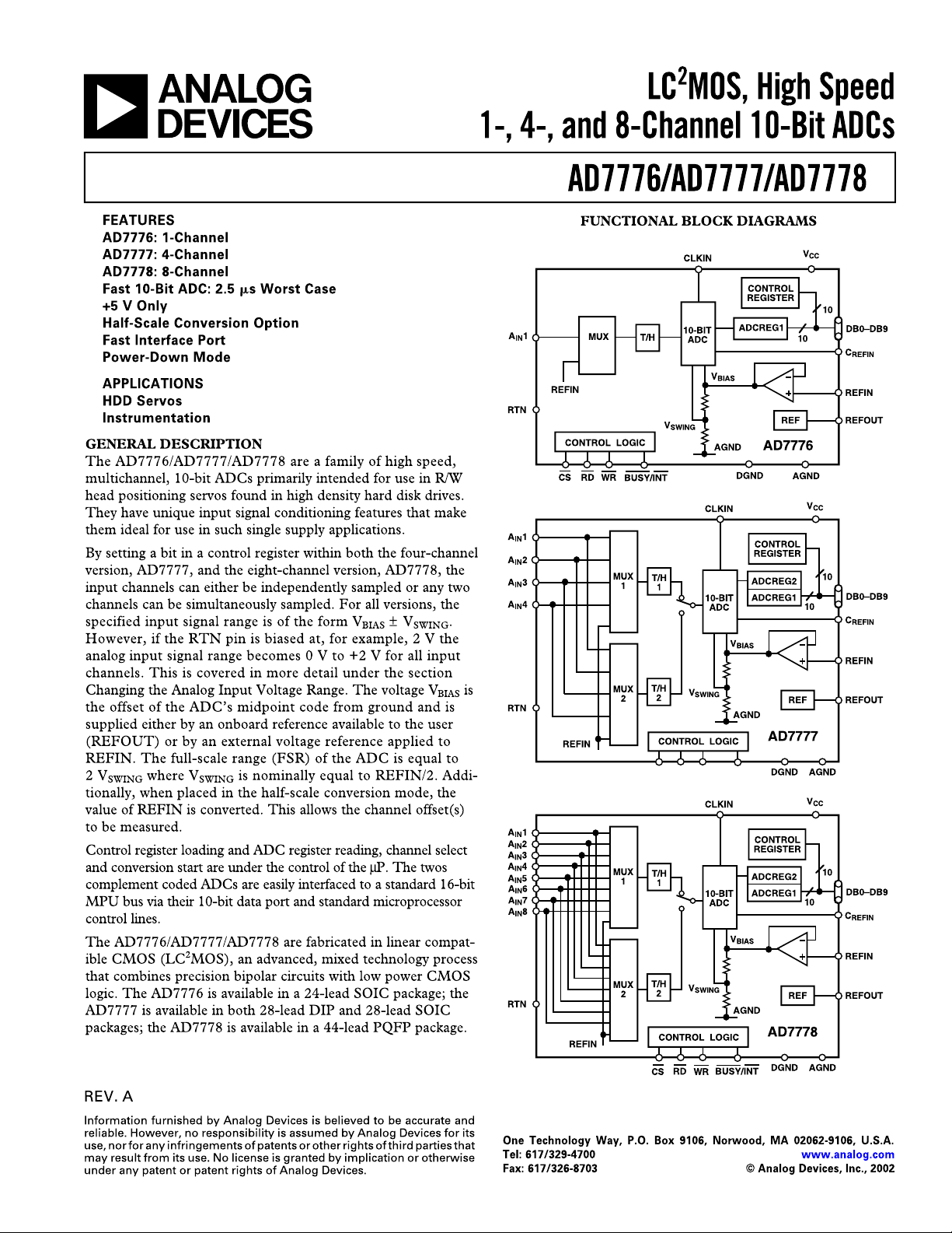
ANALOG DEVICES AD776 Service Manual


AD7776/AD7777/AD7778–SPECIFICATIONS
CLKIN = 8 MHz; RTN = O V; C
Parameter A Versions
= 10 nF; all specifications T
REFIN
to T
MIN
1
Units Conditions/Comments
unless otherwise noted.)
MAX
(VCC = +5 V ⴞ 5%; AGND = DGND = O V;
DC ACCURACY
Resolution
2
10 Bits
Relative Accuracy ± 1 LSB max See Terminology
Differential Nonlinearity ± 1 LSB max No Missing Codes; See Terminology
Bias Offset Error ± 12 LSB max See Terminology
Bias Offset Error Match 10 LSB max Between Channels, AD7777/AD7778 Only; See Terminology
Plus or Minus Full-Scale Error ± 12 LSB max See Terminology
Plus or Minus Full-Scale Error Match 10 LSB max Between Channels, AD7777/AD7778 Only; See Terminology
ANALOG INPUTS
Input Voltage Range
All Inputs V
BIAS
± V
SWING
Input Current +200 µA max VIN = V
V min/V max
BIAS
± V
; Any Channel
SWING
REFERENCE INPUT
REFIN 1.9/2.1 V min/V max For Specified Performance
REFIN Input Current +200 µA max
REFERENCE OUTPUT
REFOUT 1.9/2.1 V min/V max Nominal REFOUT = 2.0 V
DC Output Impedance 5 Ω typ
Reference Load Change ± 2 mV max For Reference Load Current Change of 0 to ± 500 µA
± 5 mV max For Reference Load Current Change of 0 to ± 1 mA
Short Circuit Current
3
20 mA max See Terminology
Reference Load Should Not Change During Conversion
LOGIC OUTPUTS
DB0–DB9, BUSY/INT
, Output Low Voltage 0.4 V max I
V
OL
, Output High Voltage 4.0 V min I
V
OH
Floating State Leakage Current ± 10 µA max
Floating State Capacitance
3
10 pF max
= 1.6 mA
SINK
SOURCE
= 200 µA
ADC Output Coding Twos Complement
LOGIC INPUTS
DB0–DB9, CS, WR, RD, CLKIN
Input Low Voltage, V
Input High Voltage, V
Input Leakage Current 10 µA max
Input Capacitance
INL
INH
3
0.8 V max
2.4 V min
10 pF max
CONVERSION TIMING
Acquisition Time 4.5 t
Single Conversion 14 t
Double Conversion 28 t
t
CLKIN
High 50 ns min Minimum High Time for CLKIN
t
CLKIN
t
Low 40 ns min Minimum Low Time for CLKIN
CLKIN
CLKIN
5.5 t
+ 70 ns max
CLKIN
CLKIN
CLKIN
125/500 ns min/ns max Period of Input Clock CLKIN
ns min See Terminology
ns max
ns max
POWER REQUIREMENTS
Range 4.75/5.25 V min/V max For Specified Performance
V
CC
, Normal Mode 15 mA max CS = RD = +5 V, CR8 = 0
I
CC
, Power-Down Mode 1.5 mA max CR8 = 1. All Linear Circuitry OFF
I
CC
Power-Up Time to Operational
Specifications 500 µs max From Power-Down Mode
DYNAMIC PERFORMANCE See Terminology
Signal to Noise and Distortion
S/(N+D) Ratio –56 dB min V
Total Harmonic Distortion (THD) –60 dB min V
Intermodulation Distortion (IMD) –75 dB typ fa = 103.2 kHz, fb = 96.5 kHz with f
= 99.88 kHz Full-Scale Sine Wave with f
IN
= 99.88 kHz Full-Scale Sine Wave with f
IN
SAMPLING
SAMPLING
SAMPLING
= 380.95 kHz
= 380.95 kHz
= 380.95 kHz. Both
Signals Are Sine Waves at Half-Scale Amplitude
Channel-to-Channel Isolation –90 dB typ VIN = 100 kHz Full-Scale Sine Wave with f
NOTES
1
Temperature range as follows: A = –40°C to +85°C.
2
1 LSB = (2 × V
3
Guaranteed by design, not production tested.
Specifications subject to change without notice.
)/1024 = 1.95 mV for V
SWING
SWING
= 1.0 V.
SAMPLING
= 380.95 kHz
–2–
REV. A

AD7776/AD7777/AD7778
TIMING SPECIFICATIONS
Parameter Label Limit at T
1, 2
(VCC = +5 V ⴞ 5%; AGND = DGND = 0 V; all specifications T
MIN
to T
Unit Test Conditions/Comments
MAX
MIN
to T
, unless otherwise noted.)
MAX
INTERFACE TIMING
CS Falling Edge to WR or RD Falling Edge t
WR or RD Rising Edge to CS Rising Edge t
WR Pulsewidth t
CS or RD Active to Valid Data
Bus Relinquish Time after RD
3, 4
3, 5
1
2
3
t
4
t
5
0 ns min
0 ns min
53 ns min
60 ns max Timed from Whichever Occurs Last
10 ns min
45 ns max
Data Valid to WR Rising Edge t
Data Valid after WR Rising Edge t
WR Rising Edge to BUSY Falling Edge t
6
7
8
55 ns min
10 ns min
1.5 t
2.5 t
CLKIN
+ 70 ns max
CLKIN
ns min CR9 = 0
WR Rising Edge to BUSY Rising Edge or
INT Falling Edge t
WR or RD Falling Edge to INT Rising Edge t
NOTES
1
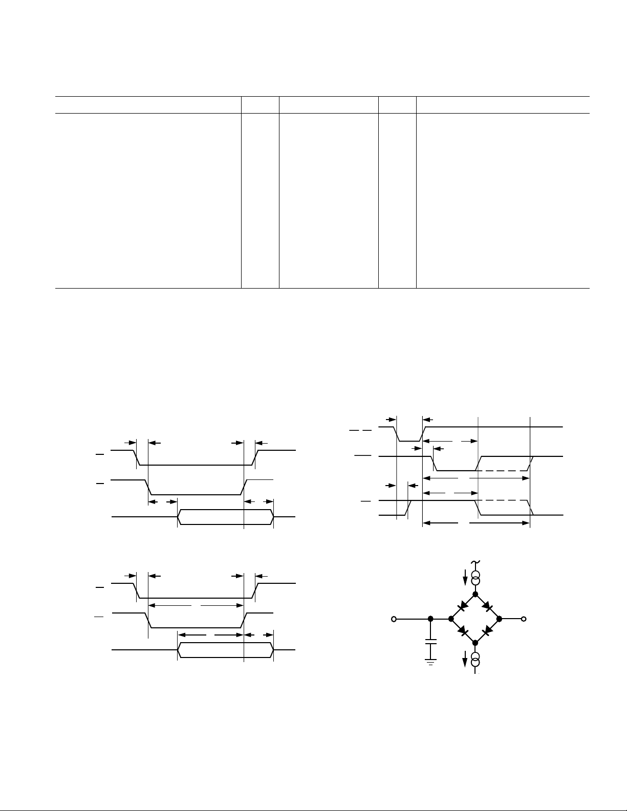
See Figures 1 to 3.
2
All input signals are specified with tr = tf = 5 ns (10% to 90% of 5 V) and timed from a voltage level of 1.6 V.
3
100% production tested. All other times are guaranteed by design, not production tested.
4
t4 is measured with the load circuit of Figure 4 and defined as the time required for an output to cross 0.8 V or 2.4 V.
5
t5 is derived from the measured time taken by the data outputs to change 0.5 V when loaded with the circuit of Figure 4. The measured time is then extrapolated back
9
t
10
11
to remove the effects of charging or discharging the 100 pF capacitor. This means that the time t5 quoted above is the true bus relinquish time of the device and, as
such, is independent of the external bus loading capacitance.
Specifications subject to change without notice.
19.5 t
33.5 t
+ 70 ns max Single Conversion, CR6 = 0
CLKIN
+ 70 ns max Double Conversion, CR6 = 1
CLKIN
60 ns max CR9 = 1
CS
RD
DB0–DB9
CS
WR
DB0–DB9
t
1
t
4
Figure 1. Read Cycle Timing
t
1
t
3
t
6
Figure 2. Write Cycle Timing
FIRST
CONVERSION
FINISHED
t
3
t
2
t
5
WR, RD
BUSY
(CR8 = 0)
INT
(CR8 = 1)
t
8
t
11
Figure 3.
t
2
DB n
t
7
C
OUT
100pF
(CR6 = 0)
t
9
t
10
t
9
t
10
BUSY/INT
Timing
I
OL
1.6mA
I
OH
200µA
SECOND
CONVERSION
FINISHED (CR6 = 1)
AD7777/AD7778 ONLY
+2.1V
Figure 4. Load Circuit for Bus Timing Characteristics
REV. A
–3–

AD7776/AD7777/AD7778
ABSOLUTE MAXIMUM RATINGS*
(TA = +25°C unless otherwise noted)
VCC to AGND or DGND . . . . . . . . . . . . . . . . . . –0.3 V, +7 V
AGND, RTN to DGND . . . . . . . . . . . . . –0.3 V, V
+ 0.3 V
CC
CS, RD, WR, CLKIN, DB0–DB9,
BUSY/INT to DGND . . . . . . . . . . . . . –0.3 V, V
Analog Input Voltage to AGND . . . . . . . –0.3 V, V
REFOUT to AGND . . . . . . . . . . . . . . . . –0.3 V, V
REFIN to AGND . . . . . . . . . . . . . . . . . . –0.3 V, V
+ 0.3 V
CC
+ 0.3 V
CC
+ 0.3 V
CC
+ 0.3 V
CC
Operating Temperature Range
PQFP Package, Power Dissipation . . . . . . . . . . . . . . 500 mW
θ
Thermal Impedance . . . . . . . . . . . . . . . . . . . . . 95°C/W
JA
Lead Temperature, Soldering
Vapor Phase (60 sec) . . . . . . . . . . . . . . . . . . . . . . . . 215°C
Infrared (15 sec) . . . . . . . . . . . . . . . . . . . . . . . . . . . 220°C
*Stresses above those listed under absolute maximum ratings may cause permanent
damage to the device. This is a stress rating only; functional operation of the device
at these or any other conditions above those listed in the operational sections of this
specification is not implied. Exposure to absolute maximum rating conditions for
extended periods may affect device reliability.
All Versions . . . . . . . . . . . . . . . . . . . . . . . . –40°C to +85°C
Storage Temperature Range . . . . . . . . . . . . –65°C to +150°C
Junction Temperature . . . . . . . . . . . . . . . . . . . . . . . . . +150°C
DIP Package, Power Dissipation . . . . . . . . . . . . . . . . 875 mW
θ
Thermal Impedance . . . . . . . . . . . . . . . . . . . . . 75°C/W
JA
Lead Temperature, Soldering (10 sec) . . . . . . . . . . . +260°C
SOIC Packages, Power Dissipation . . . . . . . . . . . . . . 875 mW
θ
Thermal Impedance . . . . . . . . . . . . . . . . . . . . . 75°C/W
JA
Lead Temperature, Soldering
Vapor Phase (60 sec) . . . . . . . . . . . . . . . . . . . . . . . . 215°C
Infrared (15 sec) . . . . . . . . . . . . . . . . . . . . . . . . . . . 220°C
Model Range Channels Option*
AD7776AR –40°C to +85°C1 RW-24
AD7777AN –40°C to +85°C4 N-28
AD7777AR –40°C to +85°C4 RW-28
AD7778AS –40°C to +85°C8 S-44
*R = SOIC, N = PDIP, S = PQFP
ORDERING GUIDE
Temperature No. of Package
CAUTION
ESD (electrostatic discharge) sensitive device. Electrostatic charges as high as 4000 V readily
accumulate on the human body and test equipment and can discharge without detection. Although
the AD7776/AD7777/AD7778 feature proprietary ESD protection circuitry, permanent damage
may occur on devices subjected to high energy electrostatic discharges. Therefore, proper ESD
precautions are recommended to avoid performance degradation or loss of functionality.
WARNING!
ESD SENSITIVE DEVICE
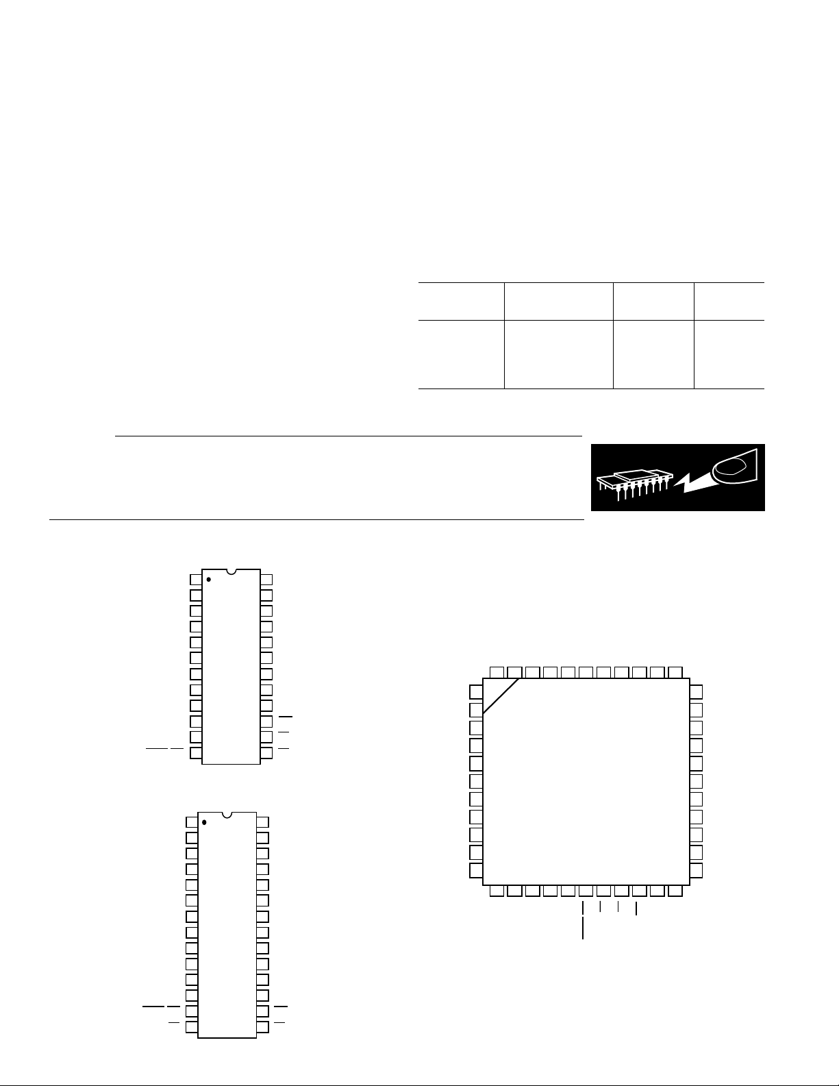
24-Lead SOIC
DB0
DB1
DB2
DB3
DGND
DB4
DB5
DB6
DB7
DB8
(MSB) DB9
BUSY/INT
1
2
3
4
5
AD7776
6
TOP VIEW
7
(Not to Scale)
8
9
10
11
12
24
23
22
20
19
18
17
16
15
14
13
28-Lead PDIP and SOIC
DB0
DB1
NC
DB2
DB3
DGND
DB4
DB5
DB6
DB7
DB8
(MSB) DB9
BUSY/INT
RD
1
2
3
4
5
6
7
AD7777
TOP VIEW
8
(Not to Scale)
9
10
11
12
13
14
NC = NO CONNECT
28
27
26
25
24
23
22
21
20
19
18
17
16
15
21
C
REFIN
AGND
RTN
REFIN
A
IN
AGND
REFOUT
V
CC
CLKIN
WR
CS
RD
C
REFIN
AGND
RTN
REFIN
AIN4
3
A
IN
2
A
IN
1
A
IN
AGND
REFOUT
V
CC
CLKIN
WR
CS
PIN CONFIGURATIONS
1 33
NC
2
NC
3
DB2
4
DB3
5
DGND
6
DB4
7
DB5
8
DB6
9
DB7
10
NC
11
NC
–4–
44-Lead PQFP
REFIN
AGND
DB1
DB0
NC
NC
NC
NC
39 38 37 36 35 3444 43 42 41 40
AD7778
TOP VIEW
(Not to Scale)
12
NC
NC
DB8
(MSB) DB9
18 19 20 21 221716151413
NC
BUSY/INT
RTN
C
CS
RD
WR
NC = NO CONNECT
REFIN
CLKIN
NC
NC
32
31
30
29
28
27
26
25
24
23
AIN8
AIN7
AIN6
AIN5
AIN4
AIN3
AIN2
AIN1
AGND
REFOUT
V
CC
REV. A
 Loading...